AlGaN/GaN High Electron Mobility Transistors with Ultra -Wide Bandgap AlN buffer
Texte intégral
Figure
Documents relatifs
according to the interferometer sweep direction, detects and corrects for fringe count errors (MIP CG1 AX), corrects for detector non-linearity (MIP CA1 AX), equalizes and
Par exemple, dans un système asynchrone (i.e., sans borne sur les délais de transmission) initialement connu avec une majorité de processus corrects, il a été montré que le
L’accès à ce site Web et l’utilisation de son contenu sont assujettis aux conditions présentées dans le site LISEZ CES CONDITIONS ATTENTIVEMENT AVANT D’UTILISER CE SITE WEB.
Based on macro-transmission measurements and simulations, the absorption coefficient of the wells is estimated to be 3 × 10 5 cm −1 (E-field ⊥ c), attesting that the oscillator
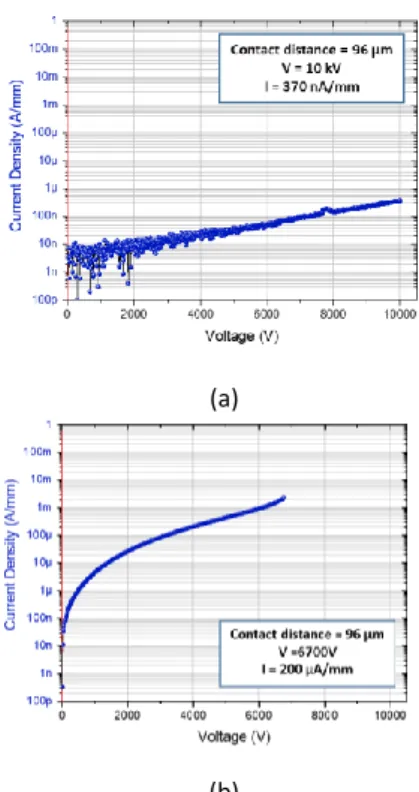
(i) the defectiveness of the AlN nucleation layer is the root cause of the leakage through an AlN/Silicon junction, and causes the vertical I-V characteristics to have a
With sharing in-plane symmetry and providing a com- positional gradient across the intermediate layers to both the epitaxial layer and the substrate, the opCG-ipVO
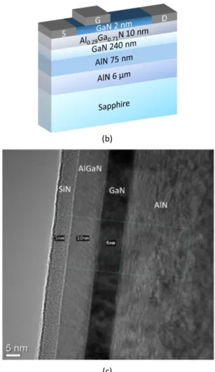
Remarkably low off-state gate and drain leakage currents below 1 µA/mm up to 3 kV have been achieved owing to the use of a thick in situ SiN gate dielectric under the gate, and a
The current-voltage (IV) characterizations performed at both room temperature and high temperature show that: (i) the defectiveness of the AlN nucleation layer is the root cause of
