HAL Id: hal-01972100
https://hal.archives-ouvertes.fr/hal-01972100
Submitted on 21 Feb 2019
HAL is a multi-disciplinary open access
archive for the deposit and dissemination of
sci-entific research documents, whether they are
pub-lished or not. The documents may come from
teaching and research institutions in France or
abroad, or from public or private research centers.
L’archive ouverte pluridisciplinaire HAL, est
destinée au dépôt et à la diffusion de documents
scientifiques de niveau recherche, publiés ou non,
émanant des établissements d’enseignement et de
recherche français ou étrangers, des laboratoires
publics ou privés.
Electron and Acoustic Phonon Confinement in
Ultrathin-Body Ge on Insulator
Vladimir Poborchii, Wen Hsin Chang, Hiroyuki Ishii, Noriyuki Uchida, Jesse
Groenen, Pavel Geshev, Toshifumi Irisawa, Tatsuro Maeda
To cite this version:
Vladimir Poborchii, Wen Hsin Chang, Hiroyuki Ishii, Noriyuki Uchida, Jesse Groenen, et al.. Electron
and Acoustic Phonon Confinement in Ultrathin-Body Ge on Insulator. International Conference on
Solid State Devices and Materials, Sep 2018, Tokyo, Japan. pp.233-234. �hal-01972100�
Electron and Acoustic Phonon Confinement in Ultrathin-Body Ge on Insulator
Vladimir Poborchii
1, Wen Hsin Chang
1, Hiroyuki Ishii
1, Noriyuki Uchida
1, Jesse Groenen
2, Pavel
Geshev
3, Toshifumi Irisawa
1and Tatsuro Maeda
11Nanoelectronics Research Institute, AIST, Tsukuba Central 4, 1-1-1 Higashi, Tsukuba 305-8562, Japan;
2CEMES-CNRS and Universite de Toulouse, 29 rue J. Marvig, 31055 Toulouse, France
3Institute of Thermophysics of the Russian Academy of Sciences, Lavrentyev Ave. 1, Novosibirsk 630090, Russia
Abstract
Recent findings show significant enhancement of both the 488nm-excitation Raman signal and the electron mo-bility as ultrathin-body Ge-on-insulator (UTB GeOI) thickness (TGeOI) scaling below 13nm [1,2]. These phe-nomena could be attributed to a quantum size effect causing a change in the Ge energy band structure. Here, we study the characteristics of electron and acoustic phonon confinement in UTB GeOI with TGeOI = 1 – 20 nm. We observe electron band gap enlargement with a decrease in TGeOI and extract E1 exciton transverse effec-tive mass value ~ 0.07 m0. Another size effect is the GeOI absorption enhancement associated with the increase in the electron density of states (DOS). For TGeOI < 5 nm, the E1(TGeOI) dependence suggests the influence of size-induced changes in the electron-phonon interaction on the E1 gap . This idea is supported by low-frequency Raman spectroscopy of GeOI confined acoustic phonons showing a significant change in acoustic phonon spec-trum at TGeOI < 5 nm,
1. Introduction
High mobility Ge-on-insulator (GeOI) structures pro-vide significant advantages in ultra-scale MOS devices such as the reduced junction leakage, the decreased parasitic ca-pacitance, and the better short-channel immunity. Recently,
high quality (001)-oriented UTB GeOI structures with pre-cise thickness control down to few nm have been fabricated with the advanced layer transfer technology called Het-ero-Layer-Lift-Off (HELLO) [1-3]. We observed a clear 488 nm (2.54 eV) excitation Raman intensity enhancement as well as a significant electron mobility enhancement in UTB GeOI with thickness TGeOI < 13 nm [1,2]. These phenomena
can be attributed to size-induced changes in Ge band struc-ture. Thus, a detailed study of size effects influencing UTB GeOI band structure is required. Here, we investigate the optical property of UTB Ge on glass to verify the effects of electron and acoustic phonon confinement.
2. Experimental and Theoretical Methods
We fabricated UTB GeOI with TGeOI = 1-20 nm on 50
µm thick transparent SiO2 substrates for investigation of the
optical properties. To evaluate Ge layer thickness, we selec-tively etched Ge layer by H2O2-based solution down to the
Al2O3 surface and measured the depth of the formed trench
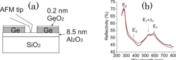
by atomic force microscopy (AFM) (Fig. 1a).
Optical reflection and transmission spectra of GeOI and bulk Ge were measured using CRAIC micro-spectrometer.
Xe lamp light was used in the 300 – 800 nm range while D2
lamp was utilized in the 250 – 320 nm range. Al mirror was used as a reflectance reference. To extract quantum con-finement effects, we compared GeOI experimental spectra with GeOI spectra calculated using optical constants of bulk Ge similar to the Si-on-oxide spectra calculation [4]. Figure 1b shows experimental and calculated reflection spectra of bulk Ge. E1 and E1+Δ1 peaks originate from the direct elec-tron transitions along the Λ ([111]) direction of the Ge Bril-louin zone (BZ). E2 peak is due to the transitions at the X-point of BZ ([100] direction) while the E’0 peak is associ-ated with transitions near the Γ-point.
Fig. 1 Cross-section view of the GeOI sample with the illustration of the GeOI thickness measurement using AFM (a); experimental (black) and calculated (red) reflection spectra of bulk Ge (b).
Raman spectra of GeOI were measured using Nano-finder 30 Raman/AFM system (Tokyo Instruments Inc.) equipped with the 561 nm wavelength laser and a set of volume Bragg grating notch filters. Calculation of acoustic phonon Raman spectra was done using photo-elastic model (PEM) [5].
3. Results
Figure 2a shows experimental reflection spectra of GeOI and bulk Ge. E1 and E1+Δ1 peaks display a blue shift with a decrease in TGeOI as expected for the band gap
en-largement due to electron confinement. However, one can see a slight red shift of 17.8 nm thick GeOI peak compared to that of bulk Ge due to light interference in the Ge layer. The interference effect is clearly presented in the theoretical GeOI reflection spectra calculated with bulk Ge optical con-stant excluding any electron confinement effect (Fig. 2b).
(a) 300 400 500 600 700 800 10 20 30 40 50 60 H~2.4nm H~1.1nm H~3.4nm H~8nm H~17.8nm R ef le ct iv ity (% ) Wavelength (nm) SiO2 Ge light Ge 300 400 500 600 700 800 0.0 0.1 0.2 0.3 0.4 0.5 0.6 0.7 1nm 10nm 20nm Re fle ct iv ity Wavelength (nm) 30nm Ge SiO2 light
Fig. 2. Experimental reflection spectra of GeOI and bulk Ge (a); theoretical reflection spectra of GeOI calculated using bulk Ge optical constants.
(a) (b)
For correct extraction of the quantum confinement ef-fect, we compared experimental and calculated absorption spectra. We measured GeOI reflection (R) and transmission (T) spectra at the light incidence from the substrate side and obtained absorption A = 100% - R-T (Fig. 3a). Such meas-urement geometry is beneficial for the GeOI absorption en-hancement compared to the geometry with the light inci-dence from the Ge layer side that is favourable for the re-flection enhancement due to high Ge/air dielectric contrast, with the transmission being equal in both geometries. Figure 3b shows experimental (black) and calculated with bulk Ge optical constants (red) absorption spectra for GeOI with TGeOI ~ 17.8 nm and ~2.4 nm. A clear blue shift is observed
for the experimental 2.4 nm thick GeOI absorption bands compared to the theoretical ones while the shift is much weaker for the 17.8 nm thick GeOI. It is important that the experimental absorption increases compared to the theoreti-cal one. This can be associated with a size-induced densi-ty-of-states (DOS) increase.
The E1 absorption feature has an excitonic origin. The
confinement-induced band gap enlargement is ΔE1 =
2(
π/TGeOI)2/2m, where is the reduced Plank’s constant
and m is the reduce mass of the exciton. According to this
model, the energy shift should display a linear dependence
on TGeOI -2. Figure 3c displays the dependence of the
meas-ured ΔE1 on TGeOI -2. The dependence displays two parts with
different slopes. For TGeOI > 5 nm, the slope reveals the
ex-citon mass m ~ 0.07m0, the projection of the 2D E1 exciton on the (001) plane being taken into account (inset in Fig. 3c). The exciton is very heavy along the Λ or [111] direction while it is rather light in the (111) plane with the transverse mass m⊥ ~0.045m0, the value close to the observed 0.07m0 confirming the quantum confinement origin of the E1 band blue shift for TGeOI > 5 nm. A decrease in the slope of the
ΔE1(TGeOI 2) dependence for TGeOI < 5 nm (Fig. 3c) suggests
that a size effect different from the electron confinement occurs. This can be a size effect in the electron-phonon in-teraction. Fig. 4a shows experimental and calculated (PEM) Raman spectra of GeOI confined acoustic phonons. For TGeOI > 5 nm, theory reasonably agrees with experiment
when the longitudinal sound velocity of bulk Ge 4.81x105 cm/sec is used, 0.2 nm GeO2 and 8.5 nm Al2O3 layers being
considered. A sound velocity reduction is required to reach
agreement with experiment for TGeOI ~ 5 nm,. With further
decrease in TGeOI, no agreement between theory and
experi-ment was obtained using PEM, probably, due to dispersion-less phonons generated by the oxide-layer-induced surface disorder. Dependence of the dominant experimental acoustic
phonon band Raman shift on 1/TGeOI (Fig. 4b) shows
devia-tion from the confinement-induced linear dependence at
TGeOI < 5 nm.
Electron-phonon interaction influences the E1 band: the lower the average phonon frequency, the stronger the contribution of acoustic phonons to the E1 band position. Recently, it was shown that the contribution of acoustic phonons to the E1 band of SOI increases with decreasing SOI thickness [6]. The change in the slope in the ΔE1(TGeOI
-2) dependence in Fig. 3c can be explained by the decrease in the average frequency of GeOI acoustic phonons and en-hancement of their contribution to the E1 band for TGeOI < 5
nm, dispersionless phonons playing an important role.
3. Conclusions
GeOI electron and acoustic phonon confinement are studied. E1 band gap and DOS increase are detected with a
decrease in TGeOI explaining the GeOI Raman enhancement
[1]. The E1 exciton transverse mass of ~ 0.07 m0 was ex-tracted from the ΔE1(TGeOI -2) dependence. The slope
de-crease in this dependence for TGeOI < 5 nm is, probably,
caused by the size-induced change in the electron-phonon interaction. Acoustic phonon Raman spectra support this. GeOI E2 and E’0 gaps study is in progress to clarify effects responsible for the electron mobility enhancement.
Acknowledgements
We thank Kakenhi grant 1 7 H 0 6 1 4 8.
References
[1] V. Poborchii et al., Appl. Phys. Lett. 108, 083107 (2016).
[2] W. H. Chang et al., IEEE Trans. El. Devic., 64, (2017) 4615
[3] T. Maeda, et al. Microel. Eng. 109 (2013) 133 [4] V. Poborchii, et al., J. Appl. Phys., 112 (2012) 074317 [5] J. Groenen, et al., Phys. Rev. B, 77 (2008) 045420
[6] V. K. Kamineni and A. C. Diebold, Appl. Phys. Lett. 99 (2011) 151903 400 500 600 700 0 20 40 60 SiO2 incident light T R R e fle ct io n /T ra nsm is si o n /A b so rp ti on ( % ) Wavelength (nm) A H=4.9 nm Ge (a)
Fig. 3. a) Transmission, reflection and absorption spectra of 4.9 nm thick GeOI; b) experimental and theoretical absorption spectra of 17.8 nm and 2.4 nm thick GeOI. Calculation was made using bulk Ge optical constants; c) ΔE1(TGeOI -2) dependence of GeOI
(squares) and its linear fitting (lines)
Fig. 4. a) experimental (black) and theoretical (red and green)) Ra-man spectra of 7.1 nm and 4.9 nm thick GeOI. Ge layer sound veloc-ity v(Ge) = 4.81x105 cm/sec like in bulk Ge was used in calculation
for TGeOI = 7.1 nm while v(Ge) = 4.81x105 cm/sec (green) and v(Ge)
= 3.81x105 cm/sec (red) for T
GeOI = 4.9 nm; b) dependence of the
dominant experimental acoustic phonon band Raman shift on 1/TGeOI.
(a) (b) 0.0 0.2 0.4 0.6 0.00 0.05 0.10 0.15 0.20 ΔE1 = 0.08 + 0.19*TGeOI-2 ΔE1 = 0.004 + 3.4*TGeOI-2 Δ E1 ( eV ) TGeOI-2 (nm-2) 0.0 0.2 0.4 0.6 0.8 1.0 1.2 10 12 14 16 18 20 22 24 Ra m an s hi ft ( cm -1) TGeOI-1 (nm-1) (c)