HAL Id: lirmm-01096047
https://hal-lirmm.ccsd.cnrs.fr/lirmm-01096047
Submitted on 16 Dec 2014
HAL is a multi-disciplinary open access
archive for the deposit and dissemination of
sci-entific research documents, whether they are
pub-lished or not. The documents may come from
teaching and research institutions in France or
abroad, or from public or private research centers.
L’archive ouverte pluridisciplinaire HAL, est
destinée au dépôt et à la diffusion de documents
scientifiques de niveau recherche, publiés ou non,
émanant des établissements d’enseignement et de
recherche français ou étrangers, des laboratoires
publics ou privés.
Efficiency of a glitch detector against electromagnetic
fault injection
Loic Zussa, Amine Dehbaoui, Karim Tobich, Jean-Max Dutertre, Philippe
Maurine, Ludovic Guillaume-Sage, Jessy Clédière, Assia Tria
To cite this version:
Loic Zussa, Amine Dehbaoui, Karim Tobich, Jean-Max Dutertre, Philippe Maurine, et al.. Efficiency
of a glitch detector against electromagnetic fault injection. DATE: Design, Automation and Test in
Europe, Mar 2014, Dresden, Germany. �10.7873/DATE.2014.216�. �lirmm-01096047�
Efficiency of a Glitch Detector against
Electromagnetic Fault Injection
Loic Zussa
∗, Amine Dehbaoui
∗, Karim Tobich
†, Jean-Max Dutertre
∗, Philippe Maurine
†Ludovic Guillaume-Sage
†, Jessy Clediere
‡, Assia Tria
‡∗Ecole Nationale Superieure des Mines de Saint-Etienne (ENSM.SE)
Gardanne, France
Email:{loic.zussa,amine.dehbaoui,jean-max.dutertre}@mines-stetienne.fr
†Laboratoire d’Informatique et de Robotique et de Microelectronique de Montpellier (LIRMM)
Montpellier, France
Email:{karim.tobich,philippe.maurine,ludovic.guillaume-sage}@lirmm.fr
‡Commissariat a l’Energie Atomique et aux Energies Alternatives (CEA)
Gardanne/Grenoble, France Email:{assia.tria,jessy.clediere}@cea.fr
Abstract—The use of electromagnetic glitches has recently emerged as an effective fault injection technique for the purpose of conducting physical attacks against integrated circuits. First research works have shown that electromagnetic faults are induced by timing constraint violations and that they are also located in the vicinity of the injection probe. This paper reports the study of the efficiency of a glitch detector against EM injection. This detector was originally designed to detect any attempt of inducing timing violations by means of clock or power glitches. Because electromagnetic disturbances are more local than global, the use of a single detector proved to be inefficient. Our subsequent investigation of the use of several detectors to obtain a full fault detection coverage is reported, it also provides further insights into the properties of electromagnetic injection and into the key role played by the injection probe.
I. INTRODUCTION
Since the early warning of Quisquater et al. in 2002 [1], the use of electromagnetic (EM) glitches has recently emerged as an effective fault injection technique for the purpose of conducting physical attacks against ICs [2], [3], [4]. These latter works indicate that the mechanism related to the injec-tion of faults involves timing constraint violainjec-tions. The timing constraint violation is induced by a transient underpowering of the target created by theEMdisturbances. This effect is highly correlated with the quality of the coupling between the supply network of the target (the victim) and the injection probe (the aggressor). Further, the underpowering seems to be more local than global: faults are located in the vicinity of the injection probe.
The novelty of this threat explains that no countermeasure dedicated to cope withEMinjection has been yet proposed (to the best of our knowledge).
There is two other common fault injection means related to timing violations: clock and power supply glitches. They both have a global effect (i.e. the disturbance affects the whole
chip). A delay-based countermeasure (CM) has been recently proposed and validated by [5] to cope with this kind of timing violation. However, the question of its efficiency against EM
glitches was to be raised. Indeed, an EM disturbance located away from the actual implementation of the CM may induce a fault without triggering an alarm.
This paper reports an evaluation of a delay-basedCMagainst
EM glitches. Because a single CM was insufficient to detect with a high level of confidence EM induced faults, we have
investigated the use of several CMs to attain this purpose. Conducting these experiments also provides many further insights into the properties ofEMinjection: how local its effect is and how the design of the injection probe may influence the process.
The contributions of this paper to that research field are:
• the disclosure of guidelines to implement a delay-based
countermeasure against EMinjection,
• a study and evidences of its local effect,
• an illustration of the key role of the injection probe, • a further assessment of the actual threat related to EM
injection.
This article is organized as follows. Section II recalls some basics related to timing violations, describes the delay-based countermeasure, and reports its efficiency against clock and power glitches. Section III describes the experimental set-up and protocol, presents the experimental results and provides an interpretation. Finally section IV concludes the paper.
II. PRELIMINARIES
This section reminds the mechanisms involved in fault injection by timing constraint violation. It also describes the principle of the delay-based countermeasure we designed to cope with this injection technique. Its efficiency against clock and power supply glitches is reported likewise.
A. Timing constraint violation
Most digital ICs use one or several synchronous clock signals to synchronize their internal operations. Data are released from launch register banks on a clock rising edge, processed by the logic, and finally latched by capture registers on the next clock rising edge. Thus, in first approximation, the clock period (Tclk) has to be greater than the largest
propagation delay of the logic (i.e. its critical time DpM ax)
to ensure correct operation. A precise writing of this timing constraint requires to take into account four other parameters: Dclk2q, the time spent by a register to release a data after the clock rising edge; Tskew, the clock skew between launch
and capture registers; Tjitter the clock jitter; and Tsetup, the
setup time of the capture register. The setup time measures the amount of time a register’s input data must be stable before the clock’s rising edge to ensure reliable operation. This constraint expressed in Eq. 1 is called the setup time constraint (note that we do not describe here the clock pulse width constraint and the hold time constraint for the sake of brevity).
Tclk> Dclk2q+ DpM ax+ Tsetup+ Tskew+ Tjitter (1)
The time margin related to eq. 1 is called the time slack (i.e. the difference between required arrival time and actual arrival time at the input data of a register). A positive slack means that eq. 1 is fulfilled, conversely a negative slack is led to its violation.
The violation of this timing constraint is a straightforward means to inject faults into a circuit. A setup time violation arises if the last signal transition is too close to the clock rising edge (TheDFF’s output undergoes a metastable behavior [6]: it may stabilize either at a high or low state. An error may occur or not). Then, increasing the stress applied to the chip, an early latching arises. There is no signal transition during the setup time and an erroneous value is latched. Hereafter, we will refer to constraint timing violation for both cases.It exists many means to obtain a timing constraint violation for the purpose of injecting faults into an IC. The most common are clock and power supply glitches that induce a transient violation of eq. 1. A clock glitch [7] consists in reducing temporarily the clock period (left handside of eq. 1) to obtain a negative slack, whereas a power glitch [8] induces a transient increase of the logic propagation times (right handside of eq. 1). The next sections report the principle of a countermeasure based on monitoring the advent of timing violations due to clock or power glitches, and some experimental validations.
B. The delay-based countermeasure
We have designed a delay-based countermeasure (CM) against timing violations from the implementation reported by Endo et al. in [5] (see also [9]). The principle of this CM
consists in detecting the violation of a guarding delay prior to any timing violation. The clock signal is used as a reference to be able to draw comparisons between the guarding delay and the clock period (Tclk). In normal operation the guarding
delay is set greater than the critical time (DpM ax), but smaller
than Tclk. By doing so, if Tclk is decreased for the purpose
of inducing a timing violation, it will have to be shorter than the guarding delay (what we call a guarding delay violation) before inducing a timing violation. Hence, if the CM is able
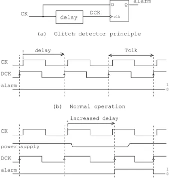
to detect this guarding delay violation, it will also be able to detect any fault injection attempt by clock glitches. Similarly, if the power supply voltage is decreased for the purpose of injecting a fault by increasing the target’s critical time, the guarding delay which depends upon the voltage supply in a similar way will be increased as well. As a consequence the violation of the guarding delay will arise and be detected first. The schematic of the CM depicted in Fig. 1-a fits with the above mechanisms. The guarding delay (denoted delay) is implemented with the circuit logic. It is used to obtain a delayed clock (denoted DCK) from the clock signal (denoted
CK) where DCK(t) = CK(t − delay). A D flip-flop (DFF) is used as a phase comparator between CK (connected to its data input) andDCK (connected to its clock input).
Tclk CK D Q clk DCK alarm delay CK increased delay power supply DCK 0 1 alarm
(a) Glitch detector principle
(b) Normal operation
(c) Power supply glitch detection DCK CK 0 1 alarm delay
Fig. 1. Delay-based countermeasure principle
The design is tuned in order to comply with the timing given in Eq. 2.
DpM ax< delay < Tclk (2)
In normal operation, as depicted in Fig. 1-b, theDFFoutput (denoted alarm) is low. Fig. 1-c illustrates the detection of a power supply glitch. As the power supply voltage is decreased the guarding delay is increased, it goes larger than Tclk. Thus
a high level is latched by the DFF on the next rising edge of DCK: the alarm is triggered at high level indicating a fault injection attempt. For the sake of brevity we have not sketched the detection of a clock glitch which is very similar. This
countermeasure was first designed to be embedded in anFPGA
running theAESencryption algorithm as described in the next subsection. We also report in subsection II-D experiments of its validity against clock and power glitches. The next section devoted to the study of the effect of EMglitches describes its efficiency against such perturbations. It will be exposed that this CM may be used likewise as a test pattern to study the local effects of EM glitches.
C. Implementation
The experiments reported in this work were carried out on anFPGA(Xilinx Spartan 700). At first, theCMwas embedded along with a hardware implementation of the AES algorithm (its 128-bits version). The device was operated at 100MHz at its nominal power supply (1.2V).
The CM primitive was implemented as a hard macro [10]. It allows to change its location within the logic slices of the
FPGAwithout modifying its actual architecture after a proper tuning of the guarding delay has been found. Furthermore, it ensured that its design was identical after each of the synthesize and routing steps we have ran. The Xilinx software ’FPGA Editor’ enables the creation of hard macros, which are manually placed, routed and configured designs, which can be instantiated multiple times in anFPGAdesign. This feature can be exploited to design an exactly defined delay based alarm and instantiate it several times.
In a second time, while studying more precisely the effect of EM glitches, several CM primitives were embedded as described in subsection III-A. Thanks to the use of hard macros, every instance of the CM was identical (however because of within-die variations [11] the various CMs may have different thresholds of triggering).
D. Clock and power supply glitches
As shown in [8] clock and power supply glitches lead to timing constraint violations that both affect the whole die (i.e. they have a global effect). Thus, a single countermeasure should be sufficient to detect any fault injection attempt related to these techniques. For the purpose of drawing comparisons while studying the effects of EM glitches, we have first carried out injection experiments by means of clock and power glitches. The experimental setup is described in Fig. 6.
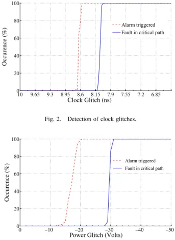
Clock glitch injections (several thousands with random data) were conducted during the9th
round of theAESby shortening progressively the corresponding clock period from 10ns to 7.2ns. As expected the alarm was always triggered prior to the injection of the first fault. Fig. 2 reports an example of the obtained results. The occurrence rates of the triggering of the alarm (in red) and of the injection of a fault (in blue) are drawn versus the clock period of the attacked round. A one hundred percent of detection was recorded before that the fault occurrence rate started to rise.
Similar experiments were made by means of negative power supply glitches of 10ns centered on the AES9thround. Alike, as shown in Fig. 3, were the occurrence rates are drawn versus
10 9.65 9.3 8.95 8.6 8.15 7.9 7.55 7.2 6.85 0 20 40 60 80 100 Clock Glitch (ns) Occurence (%) Alarm triggered Fault in critical path
Fig. 2. Detection of clock glitches.
0 −10 −20 −30 −40 −50 0 20 40 60 80 100
Power Glitch (Volts)
Occurence (%)
Alarm triggered Fault in critical path
Fig. 3. Detection of power supply glitches.
the amplitude of the power glitches, the triggering of the alarm was always prior to any fault injection.
As a result, it appeared that a single glitch detector is sufficient to protect the whole FPGA.
III. ELECTROMAGNETIC GLITCHES
This new fault injection means takes advantage of the presence of the numerous horizontal and vertical loops, in the routing of the power and ground networks, to inject sudden variations of the current flowing through. These sudden current variations produce voltage drops and ground bounces that alter the propagation of signals through the logic and therefore induce timing faults. Thus, they produce an effect similar to that of voltage glitches. However, because of the locality of theEMcoupling,EMspikes can be locally injected, anywhere, in the IC resulting in an injection that could be sufficiently local to get round a single glitch detector usually located in the neighborhood of supply pads or of the on-chip voltage regulator.
The following experiments have several goals. The first one is to characterize the spatial limitation of the aforementioned
CM. This also demonstrates the locality of EM glitches, our second goal. Finally, the last goal of these experiments is to demonstrate that handmade probes designed according to some of the recommendations of [12] are able to concentrate intense and powerful magnetic fields on reduced areas.
A. The FPGAimplementation
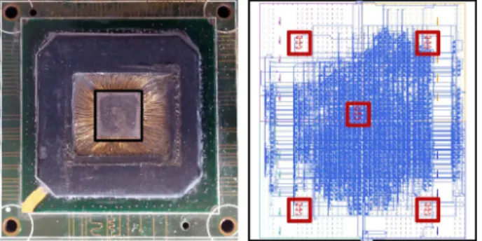
EM injection experiments were conducted on an FPGA
implementing the AES algorithm and five glitch detectors. Fig. 4-b shows the floorplan, the placement and the routing of the AES and glitch detectors mapped into the FPGA. The location of the detectors is highlighted with red squares. Fig. 4-a presents a front view of the opened device after chemical decapsulation, it allows determining the size and location of the silicon die (underlined in black). This choice was done in order to try to detect any EM glitch penetrating in the IC
at any point of the IC surface. At this point, this choice of five detectors as well as their position was done from purely geometric considerations.
Fig. 4. (a) Test chip after front side decapsulation and (b) AES (blue) and CMs (red squares) implementation within the design floor plan
B. Electromagnetic Glitch
The EMinjection probes were handmade probes. They are made up of a ferrite core end around which a copper wire is enclosed to form 4-5 turns (see Fig. 5). During the experiments two different probes were used. One, denoted ’G’, with a diameter of 3000µm and a flat tip end; the second, denoted ’F’, with a ferrite core of 500µm with a sharp tip end of diameter of300µm according to recommendations of [12]. To produce EMglitches a voltage pulse generator (4A and 20V-200V pulse capability) was adopted. It delivers pulses with a duration ranging from 10ns to 100ns to the EM probes. To access the EM glitch susceptibility of the IC as well as the efficiency of the glitch detectors, a motorized stage was used to scan theICsurface and its neighborhood using theEMglitch
Fig. 5. The two EM injection probes
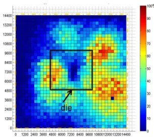
platform (see Fig. 6). The scanned area was14.4 × 14.4mm2
while the silicon die area (white square in cartographies) was 5.6×5mm2. A same displacement step of400µm was chosen
along the XY axis. At each location of the injection probe, 20
EMglitches were induced. As a result it takes about220min. to perform a full cartography.
Using this platform, several EM glitch cartographies (tar-geting theAES9thround) were launched with both probes G and F and pulses of different amplitudes were used to modify both the power and the resolution of the injections. During these cartographies, the output of the glitch detectors (alarms) as well as the ciphertexts were monitored.
C. Spatial limitation of glitch detectors
Fig. 7 displays the cartography showing the triggering rate of the alarm located in the bottom right part of the floorplan while Fig. 8 gives a cartography of the fault injection rate. Both were obtained with probe G and200V pulse amplitude. 1296 probe locations were investigated to draw the cartography, corresponding to25360EMglitches. The alarm was triggered 7308 times. From Fig. 7 one may conclude that one glitch detector is not sufficient to detect all EM glitches produced above the die (the white rectangle) and its close vicinity. From Fig. 8 one may conclude that this alarm, which was detecting absolutely all voltage or clock glitches, is not able to detect all EM glitches producing faults. There is, indeed, several locations in the right bottom part of the investigated area that have one hundred fault injection rates while having a zero detection rate. From the1935 faults actually injected, 80 were undetected. Moreover, this demonstrates that EM glitch has a local effect contrarily to voltage or clock glitches which are global.
D. Enhancing the robustness of theIC againstEMglitches The above results show that our detector has a wide, but insufficient, area of detection. Indeed all EM glitches attempts are not detected. It is therefore mandatory to integrate several detectors. This explains why five detectors have been integrated. Fig. 9 shows the detection rate of EM glitches obtained by considering the answers of the five detectors rather than the answer of a single one. The detection area was clearly
Fig. 7. Cartography of the triggering rate of the alarm - 1 detector (Probe G, pulse amplitude equal to 200V).
Fig. 8. Fault occurrence rate w.r.t. the probe tip end position (Probe G, pulse amplitude equal to 200V).
TABLE I
OVERHEAD OF THE GLITCH DETECTORS
Number Overhead of used slices
None Protected AES 2741
AES + 1 Glitch detector 2750 0.3 % AES + 5 Glitch detectors 2785 1.6 %
extended. Table I reports the overhead in terms of the area used by the glitch detectors.
E. Number of detectors
Considering the above results, one may wonder about the number of glitch detectors a designer has to integrate to secure an IC. If the answer depends of course on the quality of the detectors, it also depends on the resolution of theEMinjection probes that the adversaries may use and of the pulse amplitude
Fig. 9. Cartography of the alarm triggering rate - 5 detectors (Probe G, pulse amplitude equal to 200V).
required to inject a fault (i.e. theEMsusceptibility of the IC).
Fig. 10. Rate of triggering of at least one alarm among the five alarms with Probes G (flat tip end 3000µm) and F (sharp tip end 300µm) with pulse amplitude equal to 200V, 100V or 75V.
Indeed Fig. 10 shows the triggering rate of at least one alarm among the five alarms with probe G and F and pulse amplitudes equal to 200V, 100V or 75V while Fig. 11 gives the fault injection rates. Note that these rates are drawn according the same color scale used in previous cartographies.
25530 EMglitches were injected to draw each cartography. With probe G at 200V pulse amplitude, the alarm triggering rate (at least one alarm out of five triggered) was32%, 1995 faults were induced which were always detected. At 100V amplitude, the alarm triggering rate was21%, 1052 faults were injected.8 of these injected faults were undetected. With probe F at100V pulse amplitude, the alarm triggering rate was 6%
Fig. 11. Fault injection rate with Probes G (flat tip end 3000µm) and F (sharp tip end 300µm) with pulse amplitude equal to 200V, 100V or 75V.
and133 faults were induced from which 12 were not detected. At 75V pulse amplitude with probe F, the alarm triggering rate was 5.1% and 115 faults were induced. Five faults were undetected. The decrease of the alarm triggering rate as the pulse amplitude or the probe size were decreased was expected because a smaller voltage pulse amplitude induces a weaker
EM disturbance. However, the design of probe F makes it possible to defeat the detection capability of the five glitch detectors simultaneously with a success rate slightly above 10%.
Therefore the use of five glitch detectors may not be sufficient or their placement not optimal depending on the resolution of the injection probe. However, despite succeeding in injecting a small number of undetected faults, the feasibility of the attack is questionable. Indeed, many fault injection attempts would have been detected first and an adapted answer to that threat should have been taken [7].
One may also observe that the detection area is slightly narrower when reducing the pulse amplitude and much more narrow when the resolution of theEMprobe is enhanced. This latter experimental results confirms that the use of ferrite rods with a sharp end allows to concentrate the magnetic field on reduced surface (as expected from the simulation results of [12]) and therefore:
• to enhance the spatial resolution of EMinjection probes, • to get around efficient glitch detectors designed to detect
clock and power spikes.
IV. CONCLUSION
In this paper,EMglitch was compared to voltage and clock glitch fault injection techniques. If clock and voltage glitches can be thwarted by the use of a single delay-based glitch detector, we experimentally highlighted that the use of a single
detector may not be sufficient to thwartEMglitch based fault attacks. Additionally, we had experimentally demonstrated that the use of ferrite rods with sharp end allows enhancing the spatial resolution of the EM glitches. Finally, the efficiency
of glitch detector (based on the monitoring of delay at least) in detecting EM pulses has been pointed out. However, the number of detectors to be used as well as their optimal placement on the ICsurface remain an open problems.
ACKNOWLEDGMENT
We kindly acknowledge the french Agence Nationale de la Recherche for funding this research work with the E-MATA HARI project (ANR-12-INSE-0005) and the EMAISeCi project (ANR-10-SEGI-0012).
REFERENCES
[1] Jean-Jacques Quisquater and David Samyde. Eddy current for Magnetic Analysis with Active Sensor. In Esmart, 2002.
[2] Amine Dehbaoui, Jean-Max Dutertre, Bruno Robisson, and Assia Tria. Electromagnetic transient faults injection on a hardware and a software implementations of aes. In Fault Diagnosis and Tolerance in Cryptog-raphy (FDTC), 2012 Workshop on, pages 7–15. IEEE, 2012. [3] Amine Dehbaoui, Amir-Pasha Mirbaha, Nicolas Moro, Jean-Max
Dutertre, and Assia Tria. Electromagnetic glitch on the aes round counter. In COSADE, pages 17–31, 2013.
[4] Pierre Bayon, Lilian Bossuet, Alain Aubert, Viktor Fischer, Franc¸ois Poucheret, Bruno Robisson, and Philippe Maurine. Contactless elec-tromagnetic active attack on ring oscillator based true random number generator. In COSADE, pages 151–166, 2012.
[5] Sho Endo, Yang Li, Naofumi Homma, Kazuo Sakiyama, Kazuo Ohta, and Takafumi Aoki. An efficient countermeasure against fault sensitivity analysis using configurable delay blocks. In Fault Diagnosis and Tolerance in Cryptography (FDTC), 2012 Workshop on, pages 95–102. IEEE, 2012.
[6] J.U. Horstmann, H.W. Eichel, and R.L. Coates. Metastability behavior of cmos asic flip-flops in theory and test. Solid-State Circuits, IEEE Journal of, 24(1):146 –157, feb 1989.
[7] Sho Endo, Takeshi Sugawara, Naofumi Homma, Takafumi Aoki, and Akashi Satoh. An on-chip glitchy-clock generator for testing fault injection attacks. J. Cryptographic Engineering, 1(4):265–270, 2011. [8] Lo¨ıc Zussa, Jean-Max Dutertre, Jessy Cl´edi`ere, and Assia Tria. From
physical stresses to timing constraints violation. IOLTS 2013, 2013. [9] N. Selmane, S. Bhasin, S. Guilley, and J.L. Danger. Security evaluation
of application-specific integrated circuits and field programmable gate arrays against setup time violation attacks. Information Security, IET, 5(4):181–190, 2011.
[10] Xilinx. FPGA Editor Guide. http://www.xilinx.com/support/sw manuals/2 1i/download/fpedit.pdf.
[11] Pete Sedcole and Peter YK Cheung. Within-die delay variability in 90nm fpgas and beyond. In Field Programmable Technology, 2006. FPT 2006. IEEE International Conference on, pages 97–104. IEEE, 2006. [12] R. Omarouayache, J. Raoult, S. Jarrix, L. Chusseau, and P. Maurine.
Magnetic microprobe design for em fault attackmagnetic microprobe design for em fault attack. In emceurope, 2013.