HAL Id: cea-01635441
https://hal-cea.archives-ouvertes.fr/cea-01635441
Submitted on 15 Nov 2017
HAL is a multi-disciplinary open access
archive for the deposit and dissemination of
sci-entific research documents, whether they are
pub-lished or not. The documents may come from
teaching and research institutions in France or
abroad, or from public or private research centers.
L’archive ouverte pluridisciplinaire HAL, est
destinée au dépôt et à la diffusion de documents
scientifiques de niveau recherche, publiés ou non,
émanant des établissements d’enseignement et de
recherche français ou étrangers, des laboratoires
publics ou privés.
Integration of carbon nanotubes in silicon resonators
E. Durán-Valdeiglesias, W Zhang, A. Noury, C. Alonso-Ramos, H Hoang, S
Serna-Otálvaro, X Le Roux, E Cassan, N Izard, L Vivien, et al.
To cite this version:
E. Durán-Valdeiglesias, W Zhang, A. Noury, C. Alonso-Ramos, H Hoang, et al.. Integration of carbon
nanotubes in silicon resonators. IEEE 15th International Conference on Nanotechnology, Jul 2015,
Rome, Italy. pp.148-151. �cea-01635441�
Integration of carbon nanotubes in silicon resonators
E. Durán-Valdeiglesias, W. Zhang, A. NouryĮ, C. Alonso-Ramos, H.C. Hoang, S. F. Serna-Otálvaro,
X. Le Roux, E. Cassan, N. Izard*, L. Vivien+
1
Univ Paris 11, CNRS UMR 8622, Inst. Elect. Fondamentale (IEF), F-91405 Orsay, France +
Corresponding author: Laurent.vivien@u-psud.fr
F. Sarti, U. Torrini, M. Gurioli
Department of Physics, University of Florence European Laboratory for Non-linear Spectroscopy,
50019 Sesto Fiorentino (FI), Italy
A. Filoramo
CEA Saclay, IRAMIS, NIMBE (UMR 3685), LICSEN, Bat. 125, F-91191 Gif-sur-Yvette, Franceline 1
H. Yang, V. Bezugly, , G. Cuniberti
Technische Universitaet Dresden, Institute for Materials Science, Dresden, Germany
Abstract—This paper reports on recent results on the
integration of carbon nanotubes on the silicon photonic platform. Light coupling from carbon nanotubes in a fully integrated silicon resonator will be presented.
Keywords— Carbon nanotubes, silicon photonics, light emission, ring resonator, CMOS fabrication.
I. INTRODUCTION
Bandwidth-hungry applications such as video streaming, social networking, or web search relay on a large network of internet data centres, interconnected through optical links, to share huge amounts of information [1]. The ever-growing data rates and power consumption inside these data centres are pushing copper links close to their fundamental limits. Optical interconnects are expected to overcome these limitations, replacing electrical interconnects and becoming the preferred solution in the short link communication [2]. For instance, active optoelectronic cables are successfully commercialized by the company Luxtera since 2006 [3]. Besides, the increasing gap between the computational capacity and electrical bandwidth in high-performance computing systems is driving the development of rack-to-rack and even chip-to-chip optical links [4]. Silicon photonics [5], due to its compatibility with the CMOS platform, has been chosen by companies such as IBM [6], Intel [7] and Oracle [8] for the development of future generation photonic interconnects. However, the integration of all these photonic and optoelectronic building blocks in the same chip is very complex and is not cost-effective due to the various materials used: Ge, Si and III-V [9-11]. Indeed, the integration of a broad variety of materials on the Si platform leads to a very complex 3D integration scheme. Furthermore, III-V technology is not fully compatible with Si technology and new sophisticated processes have to be developed. The idea will be to integrate one material on the Si platform to perform all optoelectronic devices, including the source, the modulator and the photodetector. Carbon nanotubes (CNT) could be a viable solution. Indeed, CNTs are nanomaterials of particular
interest in photonics thanks to their fundamental optical properties including near-IR luminescence, Stark effect, Kerr effect and absorption. In consequence, CNTs have the ability to emit, modulate and detect light in the wavelength range of silicon transparency [12-16]. Furthermore, they are also considered as a future silicon compatible material because such a material is studied for transistor channel in the future integrated circuits.
Here, we report on the theoretical and experimental comparison of the light emission coupling from CNTs into optical resonators including strip and slot ring resonators. A theoretical and experimental analysis of the light interaction of CNTs according to the optical waveguide configurations were carried out.
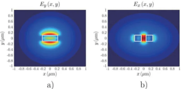
Fig. 1: a) TM mode (Electric field Ey) of strip waveguide and
b) TE mode (Electric field Ex) of slot waveguide.
II. ANALYSIS OF SILICON PHOTONIC WAVEGUIDES We analyzed the modal properties of two silicon-on-insulator (SOI) photonic integrated waveguide configurations: the strip waveguide operating with transverse magnetic (TM) polarized light [17] and the slot waveguide operating with transverse electric (TE) polarized light [18]. These two waveguides support optical modes, represented in Fig. 1, and exhibit a very large evanescent field that maximizes light-matter
Proceedings of the 15th
IEEE International Conference on Nanotechnology July 27-30, 2015, Rome, Italy
interaction outside the dielectric waveguide core. This ability to interact with the waveguide surroundings, together with their comparatively low propagation loss has made these kinds of waveguides the preferred solution in many silicon photonic biosensors [19] and an ideal platform for the investigation of the hybrid integration of CNTs onto photonic devices.
Fig. 2: Schematic views of strip and slot waveguides in a) bulk scenario, corresponding to drop casting CNT deposition and b) surface scenario, corresponding to spin coating CNT deposition.
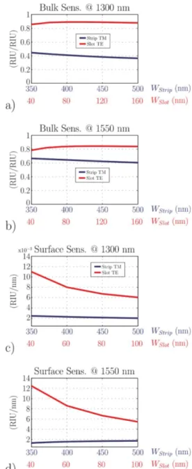
Here, we theoretically compared the light-matter interaction capability of the strip and slot waveguides considering two different scenarios that model two different CNT deposition techniques. On the one hand, we considered a bulk scenario, where we assumed that the waveguide is surrounded by a thick (semi-infinite) layer of CNTs, corresponding to drop casting deposition. On the other hand, we analyzed a surface scenario, being the waveguide covered with a thin (tCNT = 10 nm) CNT layer that assessed the spin coating deposition technique. In both cases the CNTs (surrounded by polymer for chirality selection purposes [20]) were modeled as a homogenous medium with refractive index of nCNT = 1.5. As a figure of merit we used the bulk (SB) and surface (SS) sensitivity parameters as usually defined in photonic biosensors [21]:
[
RIU
RIU
]
n
n
S
CNT eff B/
∂
∂
=
(1)[
RIU
nm
]
t
n
S
CNT eff S/
∂
∂
=
(2)where
∂
n
eff is the variation in the effective index of the waveguide mode produced either by a modification of the refractive index of the surrounding media (∂
n
CNT in bulk scenario) or a change in the thickness of the waveguide covering layer (∂
t
CNT in surface scenario). High sensitivities are directly related to strong interaction with surrounding media [21], which corresponds to the CNT-rich layer in this case.Fig. 3: Calculated sensitivity of strip and slot waveguides for bulk scenario (drop casting CNT deposition) at a) 1300 nm and b) 1550 nm wavelength and surface scenario (spin coating CNT deposition) at c) 1300 nm and d) 1550 nm wavelength.
Calculated sensitivity as a function of the main geometrical parameters of strip and slot waveguides, implemented on a 220 nm thick silicon SOI platform, is represented in Fig. 3. This analysis was performed at wavelengths of 1300 nm and 1550 nm in the center of the O and C bands of the optical fiber, typically used in telecom applications. Note that these two bands correspond to the maximum photoluminescence (PL) region of HipCo/PFO and Laser/PFO-A [22], respectively. In all studied cases slot waveguides operating with TE polarized light exhibited larger sensitivity than strip waveguides with TM polarized light. This phenomenon can be qualitatively understood looking at the strip and slot mode field distribution (Fig. 1). The optical mode in the slot waveguide is much more localized outside silicon (i.e. in the CNT-rich layer), while for strip waveguides, the mode is more confined inside the silicon core. In terms of light interaction with the CNT-rich layer, slot waveguides are thus more promising to enhance the light coupling from CNTs. However, in terms of propagation loss, strip waveguides exhibit lower loss, which induces better resonator behavior (i.e. higher Q-factors).
III. EXPERIMENTAL CHARACTERIZATION CNT INTEGRATION ON SILICON PHOTONIC MICRORESONATORS
We have integrated CNT-rich layers onto silicon photonic micro-ring resonators, implemented with strip and slot waveguides. This way we can experimentally compare the ability of such photonic structures to interact with CNTs by monitoring resonance-enhanced photoluminescence.
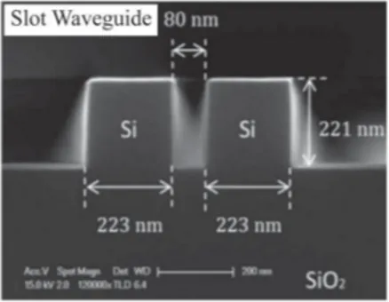
First, silicon waveguides were fabricated using e-beam lithography followed by ICP etching process. The technology developed here was optimized in order to reduce the optical propagation loss of the waveguides [23]. Figure 4 shows a scanning electron microscope(SEM) image of fabricated slot waveguides. Highly pure semiconducting HipCo CNT solution, prepared using polyfluorene-based extraction techniques [20], was deposited by spin coating. The total thickness of the PFO/CNT layer was thick enough to ensure optical mode symmetry.
Fig. 4: Scanning electron microscope (SEM) image of fabricated slot waveguides.
PL of the CNTs integrated on photonic micro-resonators is measured pumping the samples with a 735nm wavelength titanium-sapphire laser, using a microscope objective to focus the pump within the region of interest and to collect emitted PL [12]. Figure 5 represents measured light emission from CNTs coupled in strip slot waveguide resonators. We noticed that the resonances from the CNTs’ PL are more intense for the slot ring resonator approach in comparison with the emission obtained in the strip ring one. This effect can be explained by the fact that the light interaction in slot waveguides is stronger than what it can be achieved with strip waveguides. Quantitatively, this characteristic is thus in good agreement with simulation results (Fig. 1) with a stronger light interaction with slot waveguides.
Fig. 5: PL intensity as a function of the wavelength for strip and slot waveguide ring resonators. The pump wavelength was 735nm.
IV. CONCLUSIONS
In conclusion, CNTs have some remarkable optical properties which could be exploited to develop a new kind of hybrid photonics on silicon platform for a large range of applications including on-chip optical communications. We presented the latest results on the experimental demonstration of the light coupling from CNTs photoluminescence into slot waveguides and its comparison under the same measurement conditions with a strip waveguide configuration.
ACKNOWLEDGMENT
W. Zhang, S. Serna, A. Noury and H.C. Hoang acknowledge the Ministry of Higher Education and Research (France) for scholarship. This work has been supported by the European project FET CARTOON and partially by the ANR JCJC project "Ca (Re-) Lase !". The fabrication of the device was performed at the nano-center CTU-IEF-Minerve, which was partially funded by the ‘Conseil Général de l’Essonne’. This
work was partly supported by the French RENATECH network.
Į Now at ICFO-Institut de Ciencies Fotoniques, Mediterranean Technology Park, 08860 Castelldefels, Barcelona, Spain * Now at Laboratoire Charles Coulomb, CNRS-UMR 5221, Univ. Montpellier, 34095 Montpellier, France
REFERENCES
[1] H. Liu, C. F. Lam, and C. Johnson, “Scaling optical interconnects in datacenter networks,” in 18th
IEEE Symposium of High Perforfamnce Interconnects, pp. 113–116, 2010.
[2] Y. A. Vlasov, “Silicon CMOS-integrated nano-photonics for computer and data communications beyond 100G,” IEEE Commun. Mag., vol. 50, no. 2, pp. s67–s72, 2012.
[3] C. Gunn, “CMOS photonics for high-speed interconnects,” IEEE Micro., vol. 26, no. 2, pp. 58–66, 2006.
[4] L. Wosinski and Z. Wang, “Integrated silicon nanophotonics: a solution for computer interconnects,” in IEEE International Conference on
Transparent Optical Networks (ICTON). 2011, pp. 1–4.
[5] L. Vivien and L. Pavesi, Handbook of Silicon Photonics. CRC Press, 2013.
[6] S. Assefa,W. M. Green, A. Rylyakov, C. Schow, F. Horst, and Y. Vlasov, “CMOS integrated nanophotonics: enabling technology for exascale computing systems,” in OSA Optical Fiber Communications
Conference (OFC), 2011, pp. 1–4.
[7] M. Salib, M. Morse, and M. Paniccia, “Opportunities and integration challenges for CMOS-compatible silicon photonic and optoelectronic devices,” in IEEE International Conference on Group IV Photonics
(GFP), 2004, pp. 1–6.
[8] X. Zheng, F. Y. Liu, J. Lexau, D. Patil, G. Li, Y. Luo, H. D. Thacker, I. Shubin, J. Yao, K. Raj, R. Ho, J. Cunningham, and A. V. Krishnamoorthy, “Ultralow power 80 Gb/s arrayed CMOS silicon photonic transceivers for WDM optical links,” J. Lightwave Technol., vol. 30, no. 4, pp. 641–650, 2012.
[9] B. Ben Bakir, A. Descos, N. Olivier, D. Bordel, P. Grosse, E. Augendre, L. Fulbert, and J. M. Fedeli, "Electrically driven hybrid Si/III-V Fabry-Pérot lasers based on adiabatic mode transformers," Opt. Express, vol. 19, no. 11, pp. 10317-10325, 2011.
[10] L. Virot, P. Crozat, J-M. Fédéli, J-M. Hartmann, D. Marris-Morini, E. Cassan, F. Bœuf, L. Vivien, “Germanium avalanche receiver for low power interconnects,” Nature Comm., vol. 5, 2014.
[11] D. Marris-Morini, L. Vivien, G. Rasigade, J-M. Fedeli, E. Cassan, X. Le Roux, P. Crozat, S. Maine, A. Lupu, P. Lyan, P. Rivallin, M. Halbwax,
S. Laval, "Recent Progress in High-Speed Silicon-Based Optical Modulators," Proceedings of the IEEE, vol. 97, no.7, pp. 1199-1215, 2009.
[12] A. Noury, X. Le Roux, L. Vivien, and N. Izard, “Controlling carbon nanotube photoluminescence using silicon microring resonators,” Nanotechnology, vol. 25, no. 11, pp. 215201, 2014.
[13] R. Miura, S. Imamura, R. Ohta, A. Ishii, X. Liu, T. Shimada, S. Iwamoto, Y. Arakawa, and Y. Kato, “Ultralow mode-volume photonic crystal nanobeam cavities for high-efficiency coupling to individual carbon nanotube emitters,” Nat. Commun., vol. 5, 2014.
[14] E. Gaufrès, N. Izard, A. Noury, X. L. Roux, G. Rasigade, A. Beck, and L. Vivien, “Light emission in silicon from carbon nanotubes,” ACS Nano, vol. 6, no. 5, pp. 3813-3819, 2012.
[15] E. Gaufrès, N. Izard, X. Le Roux, D. Marris-Morini, S. Kazaoui, E. Cassan, L. Vivien, “Optical gain in carbon nanotubes,” Appl. Phys. Lett., vol. 96, no. 23, pp. 231105, 2010.
[16] M. Yoshida, Y. Kumamoto, A. Ishii, A. Yokoyama, and Y. Kato, “Stark effect of excitons in individual air-suspended carbon nanotubes,” Appl. Phys. Lett., vol. 105, no. 16, pp. 161104, 2014.
[17] A. Densmore, D.-X. Xu, P. Waldron, S. Janz, P. Cheben, J. Lapointe, A. Delâge, B. Lamontagne, J. Schmid, and E. Post, “A silicon-on-insulator photonic wire based evanescent field sensor,” IEEE Photon. Technol. Lett., vol. 18, no. 23, pp. 2520-2522, 2006.
[18] V. R. Almeida, Q. Xu, C. A. Barrios, and M. Lipson, “Guiding and confining light in void nanostructure,” Opt. Lett., vol. 29, no. 11, pp. 1209-1211, 2004.
[19] M.-C. Estévez, M. Álvarez, and L. M. Lechuga, “Integrated optical devices for lab-on-a-chip biosensing applications,” Laser & Photon. Rev., vol. 6, no. 4, pp. 463–487, 2012.
[20] N. Izard, S. Kazaoui, K. Hata, T. Okazaki, T. Saito, S. Iijima, N. Minami, “Semiconductor-enriched single wall carbon nanotube networks applied to field effect transistors,” Appl. Phys. Lett., vol. 92, no. 24, pp. 243112, 2008.
[21] J.G. Wangüemert-Pérez, P. Cheben, A. Ortega-Moñux, C. Alonso-Ramos, D. Pérez-Galacho, R. Halir, I. Molina-Fernández, D.-X. Xu, J.H. Schmid, “Evanescent field waveguide sensing with subwavelength grating structures in silicon-on-insulator,” Opt. Lett., vol. 39, no. 15, pp. 4442-4445, 2014.
[22] A. Nish, J.Y. Hwang, J. Doig, and R. J. Nicholas, “Highly selective dispersion of single-walled carbon nanotubes using aromatic polymers,” Nature Nanotechnol., vol. 2, no.10, pp. 640-646, 2007.
[23] W. Zhang, S. F. Serna Otálvaro, X. Le Roux, L. Vivien, and E. Cassan, “Design, fabrication and optimization of silicon slot photonic ring resonators”, in OSA Asia Communications and Photonics Conference, 2014, pp. AF1B-2.