HAL Id: hal-00394785
https://hal.archives-ouvertes.fr/hal-00394785
Submitted on 22 Jan 2019HAL is a multi-disciplinary open access archive for the deposit and dissemination of sci-entific research documents, whether they are pub-lished or not. The documents may come from teaching and research institutions in France or abroad, or from public or private research centers.
L’archive ouverte pluridisciplinaire HAL, est destinée au dépôt et à la diffusion de documents scientifiques de niveau recherche, publiés ou non, émanant des établissements d’enseignement et de recherche français ou étrangers, des laboratoires publics ou privés.
The growth of small diameter silicon nanowires to
nanotrees
P. Gentile, T. David, F. Dhalluin, D. Buttard, N. Pauc, M. den Hertog, P.
Ferret, T. Baron
To cite this version:
P. Gentile, T. David, F. Dhalluin, D. Buttard, N. Pauc, et al.. The growth of small diameter silicon nanowires to nanotrees. Nanotechnology, Institute of Physics, 2008, 19 (12), pp.19 March (2008) 125608. �10.1088/0957-4484/19/12/125608�. �hal-00394785�
Growth of small-diameter silicon nanowires to nanotrees.
P. Gentile1, T. David1, F. Dhalluin2,3, D. Buttard1, N. Pauc1, M. Den Hertog4,
P. Ferret2, T. Baron3
1CEA/Grenoble, INAC/SP2M/SiNaPS, 17 Rue des Martyrs, 38054 Grenoble 2CEA-DRT, LETI/DTS, CEA/GRE, 17 Rue des Martyrs, 38054 Grenoble 3CNRS-LTM, 17 Rue des Martyrs, 38054 Grenoble
4CEA/Grenoble, INAC/SP2M/LEMMA, 17 Rue des Martyrs, 38054 Grenoble
E-mail: pascal.gentile@cea.fr
Abstract.
In this work we have studied a way to control the growth of small diameter silicon
nanowires by the Vapour Liquid Solid (VLS) mode. We have developed a method to deposit
colloids with good density control, which is a key point for the control of the nanowires
(NWs) diameter. We also show the high dependence of the allowed growth diameter with
growth conditions opening the door to the realization of as grown 2 nm silicon NWs. Finally
we developed a smart way to realise nanotrees in the same run, by tuning the growth
conditions and making benefit of gold on the sidewall of nanowires, without two catalyst
deposition steps.
1
Introduction
The growth of semiconducting nanowires is now of a great interest for nanoelectronics, biosensors, and solar cells technology, due to their particular electrical and optical properties arising from their one dimensional geometry [1]. In particular, small diameter (d) silicon nanowires (SiNWs) and nanotrees (SiNTs) are viewed as attracting building blocks for future devices operating in the quantum limit predicted for d<5 nm wires [2,3]. To fabricate devices with homogeneous properties, getting monodispersed diameter populations is also a prerequisite. In this communication, we present a method to grow silicon nanotrees (Si NTs) with small diameter branches (<10 nm) using a two step process. This method comes from our studies which showed that (i) in case of larger diameter nanowires (> 50 nm) we have observed gold droplets on Si NWs sidewalls, based on in situ gold diffusion, (ii) the growing condition could be adjusted to grow selectively small or large NWs. By combining the catalytic activity of the Au particles at the sidewalls with the selective growth condition for different diameter we can realise NTs with branches presenting diameter down to 2 nm and
reduced size dispersion. To sum up the presented method, the first step process consists in growing large NWs (>50 nm) with Au droplets at the sidewalls and the second step consists in the selective growth of branches from these Au sidewalls droplets.
2
Experimental details
Silicon nanowires are grown by Low Pressure Chemical Vapour Deposition (LPCVD) via the VLS mechanism [4-7], in which NWs grow from gold catalyst. The silicon substrate orientation (111) is chosen to obtain vertical growth for large NWs as their growth direction is <111>. Silane (SiH4) diluted in hydrogen is used as the reactive gas. In this method, key parameters that
control the NWs characteristics are the catalyst size and the growth conditions (temperature, silane pressure). To achieve control of the catalyst size, we tested two deposition procedures, i. e. gold film dewetting and direct deposition of size calibrated catalysts from a gold colloids solution (Ted Pella) onto a silicon surface. For both methods, silicon surface is first cleaned in alcohol and deoxidized into an ammonium fluoride mixture before catalyst deposition. The first family of samples is immediately coated with a thin gold layer (< 2nm) in a joule effect evaporator, whereas “colloidal” samples are placed in an electrochemical cell for colloids deposition. In this second approach, negatively charged gold colloids (2, 5, 10, 20, 50, 100 and 200 nm diameter) dispersed in water are deposited in a controlled fashion onto the sample surface by using an external electric field as a driving force for colloids motion. This technique provides a fine control of the catalysts density over large surfaces by adjusting electrical fields or deposition times as shown in table 1. Samples are then introduced in the LPCVD reactor, and annealed under H2 flow. To form efficient catalyst from a thin gold layer, in situ annealing
(between 650°C and 850°C, 5 minutes) is required before crystal growth to induce dewetting of the films. It produces droplets with large size dispersion as compared to the colloidal way, making fine control of the diameter distribution harder. Note that for colloid deposited samples an annealing step in the 450°C - 750°C range is performed, but this treatment was not found to be critical to achieve efficient crystal growth. Temperature is then decreased down to the
growth condition and SiH4 reactive gas is introduced into the reactor, initiating the SiNWs
growth.
3
Growth modes study
In this section, growth studies are carried out to obtain (i) large diameter (> 50 nm) nanowires with Au at the sidewalls, (ii) very small diameter NWs diameter (< 10 nm) and (iii) nanotrees using a combination of the former points.
3.1 Large diameter nanowires
Optimum growth conditions for regular and vertical growth of large diameter NWs (from d> 50 nm to d≈ 1 µm, see in figure 1) on gold coated Si(111) were obtained for temperature between 550°C to 650°C and H2 and SiH4 flow rates of 4 l/mn and 10 to 25 standard cube cm
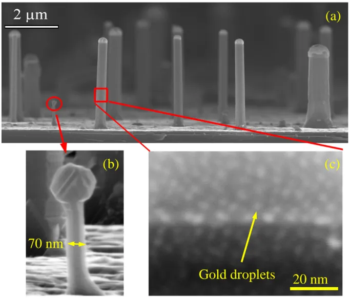
per minute (sccm) respectively. The total base pressure was held at 20 mbar. The same conditions are used for monodispersed colloidal catalyst and a high growth yield for d>50 nm is demonstrated. For these conditions, we noticed (i) an inhibited growth of small (less than 70 nm diameter) NWs’ diameter (see figure 1b) and (ii) the formation of gold droplets (d≈5-10 nm) at the sidewalls NWs as shown by the bright spots on the high magnification SEM view in figure 1c, which is corroborated by the observation from J. B. Hannon et al [8]. Size homogeneity and chemical composition of these nanodroplets have been also studied by Scanning Transmission Electron Microscopy (STEM) and Energy Dispersive X-ray (EDX) analysis [9], which confirmed the gold content in these nanodroplets and their tight size distribution. We want also to point out the fact that the growth of some NWs stops as shown in figure 1b. We attribute this effect either to the gold depletion at the Au/Si catalyst during SiNWs growth for the used experimental conditions (temperature, silane partial pressure) as shown by J. B. Hannon et a l [8] or by a poisoning of the Au/Si catalyst. This effect sets the lowest NWs’ diameter for fixed temperature and silane partial pressure independently on the size of the original Au catalyst . We found that this phenomenon is not dependant on the fabrication method of the catalyst (dewetted films or colloids). Increasing the growth temperature favours large diameter NW growth (in agreement with temperature activated diffusion of gold) and high growth rate.
3.2 Small diameter nanowires
To reduce the gold diffusion the growth temperature (TG) was decreased and in the same
time the silane flux was enhanced to conserve an equivalent growth rate. Then w e found that decreasing the TG and enhancing the silane flux give the best results to grow small diameter
NWs. To study the diameter dependence of SiNWs as a function of the growth conditions, we used various size gold colloids (2, 5, 10 20 and 50 nm diameter) and we varied the TG and silane
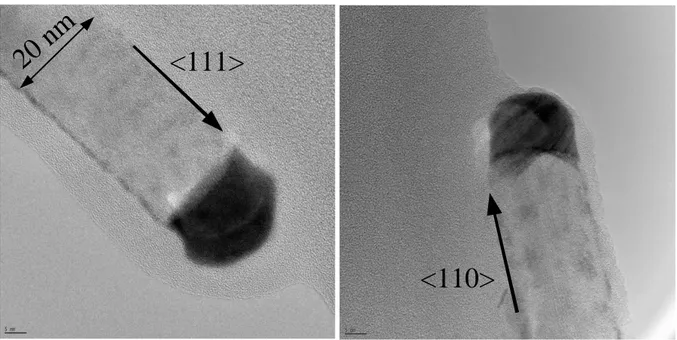
flow. SEM side views of SiNWs synthesized with 50 nm colloids are reported in figure 2 for some typical process points. We observe inhibited growth and catalyst loss on the top of NWs at 600°C and 10 sccm silane flux (figure 2(a)). The growth efficiency increased progressively as temperature decreased and silane flux increased as indicated by the following series: 550°C/silane 20 sccm (figure 2b), 450°C/silane 20 sccm (figure 2c). For smaller diameter colloids (2 nm to 20 nm), we found optimum growth conditions for lower temperatures (in the 400°C to 500°C range) and silane flux in the 35 sccm to 200 sccm range as shown in table 2. Low temperature and rich silane atmosphere are then necessary conditions to get small diameter nanowires. High resolution transmission electron microscopy (HRTEM) images are realised on 20 nm SiNWs (figure 3). These two images show crystalline nanowires with different growth direction <111> and <110> [7].
Adjusting the temperature and the silane partial pressure leads to a controlled growth of ultra small NWs diameter as seen in the figure 4. The size dispersion observed is one to three times the nominal diameter of the gold colloids corresponding to the size dispersion of the gold colloids solution. This suggests that for the small diameter conditions no catalyst diffusion and coalescence occur onto the sample at the annealing step, making the starting diameter of the wires only dependent on the colloids size dispersion. Using small diameter calibrated colloids, NWs as small as 2 nm in diameter were routinely synthesised, which opens up the door to the realisation of devices where quantum effects play a significant role. It is worthwhile noting that our method offers a straightforward way to get ultra-small NWs without the need to reduce the diameter by thermal oxidation in an uncontrollable fashion for these nano structures [10].
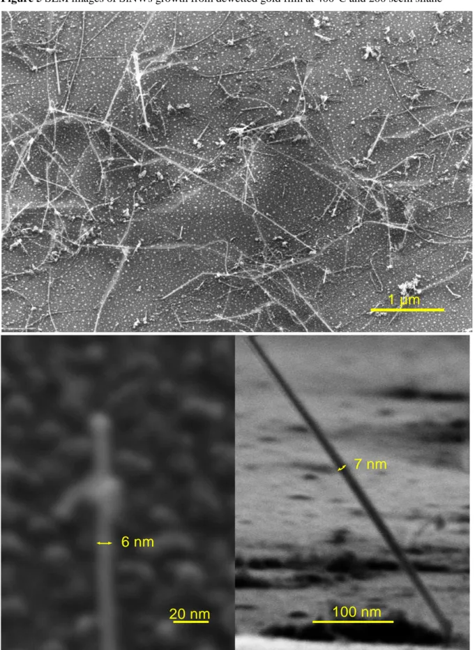
To conclude this study, we carried out similar experiments on gold coated samples and found the same NW diameters evolution with the temperature and the silane partial pressure (PSiH4). As an example, we grew SiNWs under small diameter con ditions (400°C and 200 sccm
silane) from a dewetted 0.7 nm gold film. We obtained a population of small NWs with diameters ranging from 5 nm to 50 nm (see figure 5). Note that low annealing temperatures are required to obtain small diameter NWs due to the limited ripening of gold droplets, which results in small diameter catalysts.
3.3 Discussion
To sum up the influence of the experimental conditions, a high TG and low PSiH4 leads to
the growth of large NWs diameter, whereas small NWs diameter are only form ed at low TG and
high PSiH4. In addition, we want to point out that growth of NW from large diameter catalysts
under small diameter conditions produces not only large diameter wires but also small specimens at their base (see in figure 6), making thermodynamic conditions leading parameters for the growth diameter. We propose two mechanisms to explain this result based on the formation of small catalyst. First, during the annealing phase, the large colloids particles (50 nm) could separate and form also small particles. Second, under high PSiH4 and low TG, a local
Si supersaturation in the large Au particle could be obtained and formed an efficient seed for the growth of small Si NWs. Indeed, by reducing TG, the Si diffusion length is reduced leading to
the formation of Si rich Au/Si droplets at the surface of the Au particle. Then in these two cases, at high PSiH4 these droplets have a radius superior to the critical radius necessary for the
occurence of Si NWs growth [11].
3.4 Nanotrees
From the combination of (i) the presence of small gold droplets on the sidewalls on the NWs for the larger diameter growth conditions and (ii) the selective control of growth conditions for small diameter, we propose a way to grow nanotrees with NWs branches presenting very small diameter (<10 nm) without post-growth catalyst deposition. Up to now [12,13], growth of nanotrees is a two steps process which combines initial catalyst deposition for the trunk growth
and a post-growth deposition of seeding material on as grown trunk sidewa lls to generate the catalyst for the branches growth.
In our method, at first, trunks are made under large diameter growth conditions (high temperature, low silane partial pressure) from 200 nm gold colloids to obtain 200 nm diameter SiNWs. The selectivity of the process we have developed allow us to grow a low dispersed NWs population in diameter for every kind of diameter. Growth conditions are then changed within the same run (low temperature, high silane partial pressure) to favour growth of small NWs diameter in order to get branches from the gold diffused droplets on the trunk sidewalls. Figures 7a and 7b show a typical view of a nanotree, with a 200 nm diameter trunk and branches with diameters lower than 10 nm. The branch diameter distribution is re markably restricted within the 5 nm to 10 nm range, which fits with the size of the gold droplets as shown in figure 1c and unambiguously proves that diffused droplets catalyse the branch growth.
By using colloidal particle or patterned metal as catalyst for the trunk growth, branches growth occurs only on nanowires and not on substrates, as it is the case for already published method where a two steps catalyst deposition leads to uncontrolled growth over the entire free surface [12,13]. This parasite growth must be eliminated by an ex-situ process [13]which uses a polymer mask at the trunk base to remove the redeposited catalyst from the free surface by lift-off. In addition, our method offers a single run process to produce large amounts of nanotrees with small SiNWs diameter branches with a low size dispersion, without supplemental oxidation and contamination problems resulting from air exposure and catalyst redeposition processes (in case of ex-situ processing). Similarly, we also obtained nanotrees on gold dewetted samples, but we noticed gold droplets formation on the whole sample surface presumably due to the large amount of deposited catalyst and here small diameter NWs grow on the free surface during the second growth step.
In figure 7a, we also observed a striking phenomenon: branch growth is accompanied by simultaneous regrowth at the trunk summit of a branch free section. Indeed, as shown in figure 6, under small diameter (<10 nm) growth conditions we also obtained a growth of larger NWs diameter. This demonstrates that no gold droplet forms on the regrowth section since no branch
is observed at the tree summit. Moreover, we noticed a diameter reduction of the summit in comparison with the underlying trunk section. This remarkable size modification is probably due to the reduction of the catalyst diameter during the temperature ramp down at the end of the trunk growth (silane flow stopped, H2 atmosphere). Gold free NW sidewalls in the regrowth
section obtained at lower process temperatures contrast with the rich gold trunk sidewalls seen at high temperatures. This trend suggests a thermally assisted diffusion mechanism of gold as the origin of the trunk section reduction and as the source of the catalyst droplets along the trunk sidewalls.
4
Conclusion
In summary, we have fabricated SiNWs down to 2 nm diameter and we have demonstrated different modes for SiNW growth in the gold assisted VLS method. By modulating and adjusting the growth conditions within the same run, we have developed a new and origin al method to synthesize nanotrees without the need for a second catalyst deposition to seed the branches. Our results indirectly give evidence of diffusion and formation of gold nanodroplets on the SiNWs sidewalls with a uniform and small (lower than 10 nm) diameter. Further studies and thermodynamic calculation are needed to explain these different growth modes [11] for improving the size distribution, density and length of branches.
Keywords:
Chemical vapour deposition• nanowires • Silicon •
[1] P. Noé, J. Guignard, P. Gentile, E. Delamadeleine, V. Calvo, P. Ferret, F. Dhalluin,and T. Baron, J. Appl. Phys 2007,102, 1
[2] C. Delerue, G. Allan, and M. Lannoo, Phys. Rev. B 1993,48, 11024.
[3] J. von Behren, T. van Buuren, M. Zacharias, E. H. Chimowitz, and P. M. Fauchet, Solid State Commun. 1998,105, 317.
[4] R. S. Wagner and W. C. Ellis, Appl. Phys. Lett. 1964,4, 89.
[5] R. S. Wagner, W. C. Ellis, K. A. and S. M. Arnold, J. Appl. Phys. 1964,35, 2993. [6] W. Schmidt and U. Gösele, Science 2007, 316, 698
[7] W. Schmidt, S. Senz and U. Gösele, Nano Lett. 2005, 5, 931
[8] J. B. Hannon, S. Kodambaka, F. M. Ross, and R. M. Tromp, Nature (London) 2006,440, 69 [9] M I den Hertog, J L Rouviere, F Dhalluin, P Gentile, P Ferret, C Ternon, T Baron, Inst.
Phys. Conf. Ser. Microscopy of Semiconducting Materials, Camebridge, 2 -5 april 2007 [10] C. C. Büttner, M. Zacharias, Appl. Phys. Lett. (2006), 89, 263106,
[11] F. Dhalluin, P.J. Desré, M.I. Den Hertog, J.-L. Rouvière, P. Ferret, P. Gentile and T. Baron, J. Appl. Phys. 2007,102, 094906.
[13] K.A. Dick, K. Deppert, L.S. Karlsson, W. Seiffert, L. R. Wallenberg, L. Samuelson, Nano Lett. 2006, 6, 2842
Figure 1 SEM images of SiNWs grown at 650°C, 20 mbar, silane 15 sccm, (b) zoom of small diameter NWs with stopped growth during process, (c) zoom of NWs sidewall showing gold droplets.
20 nm
Gold droplets
70 nm
(a)
Figure 2 SEM images of SiNWs grown from 50 nm gold colloids. a) growth at 600°C and silane 10 sccm. b) 550°C and silane 20 sccm. c) 450°C and silane 20 sccm.
200 nm
(a)
200 nm
(b)
200 nm
(c)
Figure 3 HRTEM images of two SiNWs. The NWs diameters are 20nm, with two different growth direction >111> and <110>.
<111>
<110>
20 n
m
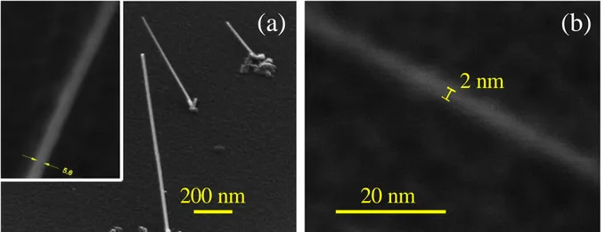
Figure 4 SEM images of SiNWs grown from gold colloid catalyst. (a) 5 nm gold colloids and,
measure was made on the inset zoom, (b) 2 nm gold colloids at low temperature and silane high partial pressure.
200 nm
(a)
20 nm
(b)
2 nm
Figure 5 SEM images of SiNWs growth from dewetted gold film at 400°C and 200 sccm silane
20 nm
1 µm
100 nm
7 nm
6 nm
Figure 6 SEM image of SiNWs grown from 50 nm diameter gold colloid catalyst at 430°C and 50 sccm silane. We can observe small diameter NWs (from 5 nm to 10 nm) at the base of the larger NWs.
1 µm
50 nm diameter colloid
Small diameter NWs
Figure 7 SEM images of nanotrees grown from 200 nm diameter trunks. The branches are grown from gold droplets present on the trunk sidewall. In (a) we can see the overgrowth NW on the top with diameter reducing, in (b) zoom of nanotree.
2 µm
1 µm
regrowth zone
Table 1 (1) Density of 50nm gold colloids as function of applied voltage for 2nm.
1 Density as function of Applied Voltage for 50 nm and 2mn colloids
Voltage (V) 0 20 30 40 50 60
Density (cm-3) 0,00E+00 2,50E+08 5,00E+08 6,00E+08 8,00E+08 1,10E+09
2 Density as a function of time for 20nm colloids and 40V
Time (mn) 0,5 1 2 4 6 10
Table 2 Growth temperature and silane flux for the different nanowires diameters.
diameter (nm) 2 5 10 20
Temperature °C 400 - 430 400 - 430 430 - 450 450 - 500 silane flux (sccm) 200 100 - 200 100 -50 50 -35