HAL Id: hal-00633002
https://hal.archives-ouvertes.fr/hal-00633002
Submitted on 17 Oct 2011
HAL is a multi-disciplinary open access
archive for the deposit and dissemination of
sci-entific research documents, whether they are
pub-lished or not. The documents may come from
teaching and research institutions in France or
abroad, or from public or private research centers.
L’archive ouverte pluridisciplinaire HAL, est
destinée au dépôt et à la diffusion de documents
scientifiques de niveau recherche, publiés ou non,
émanant des établissements d’enseignement et de
recherche français ou étrangers, des laboratoires
publics ou privés.
Tantalum superconducting tunnel junctions for infrared
photon counting
Corentin Jorel, Jean-Claude Villegier, Philippe Feautrier, Alain Benoit
To cite this version:
Corentin Jorel, Jean-Claude Villegier, Philippe Feautrier, Alain Benoit. Tantalum superconducting
tunnel junctions for infrared photon counting. Nuclear Instruments and Methods in Physics Research,
Elsevier, 2004, 520, pp.516. �10.1016/j.nima.2003.11.302�. �hal-00633002�
Elsevier Science 1
Tantalum Superconducting Tunnel Junctions for InfraRed photon
counting
Corentin Jorel,
a,b,*Jean-Claude Villégier,
bPhilippe Feautrier,
aAlain Benoit
caLAOG, 414, Rue de la piscine, Domaine Universitaire, 38040 Grenoble Cedex 9, France bCEA-Grenoble SPSMS-LCP, 17, Rue des Martyrs, 38054 Grenoble Cedex 9, France
cCRTBT, CNRS BP-166, 38042 Grenoble cedex 9, France
Elsevier use only: Received date here; revised date here; accepted date here
Abstract
Superconducting Tunnel Junctions (STJ) are currently being developed as photon detectors for a wide range of applications. Interest comes from their ability to cumulate photon counting with chromaticity (i.e. energy resolution) from the Near InfraRed (NIR) to the X rays wavelengths and excellent quantum efficiency up to 80%. Resolving power can reach more than 10 in the visible. Our main goal is to use STJ for astronomical observation at low light level in the near infrared.
This paper relates mainly to two points : The improvement of the Tantalum absorber epitaxy and the development of a new version of the fabrication process for making Ta/Al-AlOx-Al/Ta photon counting STJ. The main features of this process are that pixels have aligned electrodes and vias patterned through a protecting SiO2 layer. This vias are then used to contact the top electrode layer. We use a double thin aluminum trapping layer on top of a 150 nm thick Ta absorber grown epitaxially. © 2001 Elsevier Science. All rights reserved
keywords: STJ, Epitaxial sputtering, Tantalum, photon counting, astronomy, near infrared
PACS: the PACS codes can be found at the home page of NIMA (left column, under Contents Services):
http://www.elsevier.nl/inca/publications/store/5/0/5/7/0/1/
———
* Corresponding author. Tel.: 33 4 38 78 97 58; fax: 33 4 38 78 50 96; e-mail: [email protected].
1. Introduction
Superconducting Tunnel Junctions (STJ) have shown their capability to count photons in the NIR with a moderate energy resolution [1]. Astronomers now use STJ as photon counting cameras having intrinsic and moderate energy resolution [2].
The aim is to investigate the interest of this kind of detectors for astronomical applications and compare them to Hot Electron Bolometers devices (or Superconducting Single Photon Detectors, SSPD) that are also developed in our group [3]. Since the conventional detector arrays based on semi-conductor devices have progressed recently toward the direction of photon counting detectors [4], some niches have to be found for this type of detectors where
Elsevier Science
2
conventional devices cannot compete. The expected astronomical applications that would be investigated are wave front sensing detectors for adaptive optic system and interferometry (fringes sensors, focal plane instrument).
2. Junctions fabrication
We have developed an original fabrication process of Ta (150 nm) /Al-AlOx(1nm)-Al (80 nm)/ Ta (120 nm) superconducting junctions. The multilayer is deposited in-situ by DC-Magnetron sputtering except for the aluminum oxide barrier, which is obtained by static oxidation (200 mbar of pure O2 atmosphere during 30 minutes). R-plane polished Sapphire is used as substrate since the square section presented on surface is particularly adapted to the cubic lattice of Ta and Nb. Since the Al energy gap is smaller than the Ta one (0.172 and 0.664 meV), the two aluminum layers are used to support the localization of the excited charges near the oxide barrier [5].
2.1. Absorber epitaxy improvement
Like a majority of photon counting detectors, STJ converts the incident energy into an excited charge population which gives an access to the deposited energy. Here, the photon-excited charges tunnel through the oxide barrier and the energy can be measured thanks to the integration of the induced current. Thus, the crystalline quality of the base Ta electrode (the absorber), in which the photons are absorbed, is a critical parameter and we need to maximize the lifetime of the excited charges.
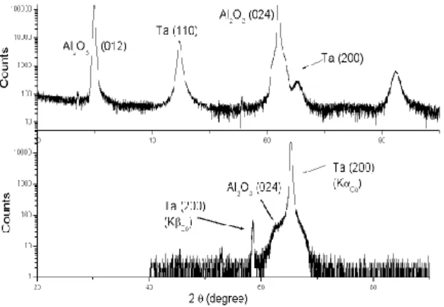
Standard Ta sputtering on Nb buffer layer [6], in a background pressure of about 10-7 mbar and at room temperature, gives polycrystalline film as shown on upper -2 scan (see Fig. 1). By sputtering at 600 °C directly on sapphire, the film is more textured, but the orientation inside the growth plan is still too dispersed and diffraction peak intensity not improved [7]. Thus, we also use a thin Nb buffer layer (<10 nm) and high substrate temperature to nucleate the right cubic Ta phase (this buffer layer facilitates the relaxation of the cubic Ta lattice constant). We obtained a very significant improvement of the diffraction peak intensity. Thanks to Scherrer law, we
estimate grains’ highness to 90 nm and Ta (200) scan gives angular dispersion of 0.3° with the growth axis.
The RRR measurement (Relative Resistive Ratio) confirms the improvement of the Ta quality: mean free path under 10K is increased by a factor 10 (l10k = 160 nm) [7].
2.2. Development of a dry etching process
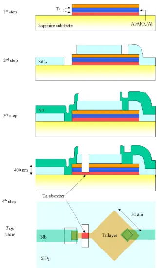
The first four steps of this new process are detailed in the Fig. 2. The junction and absorber areas are defined together during the first step of this process by RIE (Reactive Ion Etching) for Tantalum and Ion Milling for Aluminum. Immediately after, an MgO/SiO2 (400 nm) insulating film protects the entire wafer. The electrical contacts to the two junction electrodes are defined by holes etched by RIE into the SiO2 film (1 nm MgO is used as etch stop and is etched by ion milling). With the third mask level, a Nb contact level is patterned also by RIE providing current leads and contact pads used for the junction connection to the electronics.
Then, the contact to the absorber layer is forced by the etching of a small band (3 m wide) of the Ta/Al-AlOx-Al films. The etching process stops at the Ta absorber film.
Fig. 1. -2Scan of Ta Thin Film. Up: polycrystalline sputtered at room temperature. Down: Epitaxial at 600°C. Both on an Nb
Elsevier Science 3
The main motivation for developing a new process compared to the previous one [7] are : The junctions passivation just after their definition
which insures protection all along the process in the same logic as in advanced planarization techniques used in microelectronics.
The exclusive use of controlled dry etching techniques rather than lift-off ones.
The alignment of the two electrodes during the first step etching which reduce the absorber exposed surface states .
3. Conclusion
A dry etching version of the process has been developed for the fabrication of Ta-based STJ to be used as photon counting detectors for astronomical applications. The tantalum superconducting quality has been significantly improved by the introduction of a niobium buffer layer and reaches high quality epitaxy.
The results of the first wafers fabricated with this new process are promising despite we still have to optimize the oxidation conditions. They validate the different process steps and assure the feasibility of STJ with it. This process improve the quality, the reliability and the wafer homogeneity of the junction fabrication. The produced Ta STJ’s will be tested as photon counting devices and evaluated in the framework of astronomical instrumentation. They will also be compared to other superconducting devices (SSPD) that are produced in our group.
References
[1] A Peacock et al., Nature 381 (1996) 135. [2] P. Verhoeve, Proc. of LTD9 (2001). [3] Bertrand Delaet et al, this conference.
[4] C.D Mackay, R. Bell, D. Burt, P. Jerram, I. Moody, Proc. SPIE 4306 (2001) 289.
[5] N.E.Booth, Appl. Phys. Lett. 50 (1987) 293.
[6] D.W. Face et al, Journal of Vacuum Science and Technology
A5 (1987) 3408
[7] Philippe Feautrier et al, Proc. of LTD9 (2001). Fig. 2. The different process steps (side view) and top view of