HAL Id: hal-03031939
https://hal.archives-ouvertes.fr/hal-03031939
Submitted on 30 Nov 2020
HAL is a multi-disciplinary open access
archive for the deposit and dissemination of
sci-entific research documents, whether they are
pub-lished or not. The documents may come from
teaching and research institutions in France or
abroad, or from public or private research centers.
L’archive ouverte pluridisciplinaire HAL, est
destinée au dépôt et à la diffusion de documents
scientifiques de niveau recherche, publiés ou non,
émanant des établissements d’enseignement et de
recherche français ou étrangers, des laboratoires
publics ou privés.
properties for photoelectrochemical cells
Lipin Chen, Mahdi Alqahtani, Christophe Levallois, Antoine Létoublon, Julie
Stervinou, Rozenn Piron, Soline Boyer-Richard, Jean-Marc Jancu, Tony
Rohel, Rozenn Bernard, et al.
To cite this version:
Lipin Chen, Mahdi Alqahtani, Christophe Levallois, Antoine Létoublon, Julie Stervinou, et al..
As-sessment of GaPSb/Si tandem material association properties for photoelectrochemical cells. Solar
Energy Materials and Solar Cells, Elsevier, 2021, 221, pp.110888. �10.1016/j.solmat.2020.110888�.
�hal-03031939�
Assessment of GaPSb/Si tandem material association properties for
photoelectrochemical cells
Lipin Chen1, Mahdi Alqahtani 2,4, Christophe Levallois1, Antoine Létoublon1, Julie Stervinou1, Rozenn Piron1, Soline Boyer-Richard1, Jean-Marc Jancu1, Tony Rohel1, Rozenn Bernard1, Yoan Léger1, Nicolas Bertru1, Jiang Wu2, Ivan P.
Parkin3, Charles Cornet1* 1
Univ Rennes, INSA Rennes, CNRS, Institut FOTON – UMR 6082, F-35000Rennes, France
2
Department of Electronic and Electrical Engineering, University College London, London WC1E 7JE, United Kingdom
3Department of Chemistry, University College London, London WC1H 0AJ, United Kingdom
4
King Abdulaziz City for Science and Technology
⋆E-mail: Charles.Cornet@insa-rennes.fr
Here, the structural, electronic and optical properties of the GaP1-xSbx/Si tandem materials association are
determined in view of its use for solar water splitting applications. The GaPSb crystalline layer is grown on Si by Molecular Beam Epitaxy with different Sb contents. The bandgap value and bandgap type of GaPSb alloy are determined on the whole Sb range, by combining experimental absorption measurements with tight binding (TB) theoretical calculations. The indirect (X-band) to direct (Γ-band) cross-over is found to occur at 30% Sb content. Especially, at a Sb content of 32%, the GaP1-xSbx alloy reaches the desired 1.7eV direct bandgap, enabling efficient
sunlight absorption, that can be ideally combined with the Si 1.1 eV bandgap. Moreover, the band alignment of GaP1-xSbx alloys and Si with respect to water redox potential levels has been analyzed, which shows the GaPSb/Si
association is an interesting combination both for the hydrogen evolution and oxygen evolution reactions. These results open new routes for the development of III-V/Si low-cost high-efficiency photoelectrochemical cells.
Keywords: solar water splitting; III-V/Si photoelectrode; tandem material; 1.7/1.1eV bandgap combination; band alignment
1. Introduction
The conversion of solar energy into green hydrogen fuel is one significant milestone on the road to a sustainable energy future [1,2]. Especially under the current background of global energy and environmental crisis, the development of the photoelectrochemical (PEC) water splitting technology, where the sunlight falling on the semiconductor photoelectrode immersed, turns the liquid water into gaseous storable hydrogen that can be reused on demand for heat or electricity production, has driven much research in the past years [3].
However, numbers of challenges remain for the development of this technology, in terms of efficiency, profitability and sustainability. These challenges include many aspects such as the limitation of corrosion or photo-corrosion processes, the optimization of the design for solar energy harvesting, or the improvement of charge carriers transport properties in the semiconductor photoelectrodes. At the heart of the photoelectrochemical conversion process is the choice of an appropriate photoelectrode material with both good bandgap and good band alignment to harvest the largest portion of the solar spectrum and provide sufficient voltage to accomplish the water splitting reactions [4]. Due to the broadness of the solar spectrum, from infrared to ultra-violet light, the needs for combining monolithically different materials with different bandgaps and thus absorbing different wavelengths, is considered today as the main pathway to reach high solar-to-hydrogen (STH) conversion efficiency [5,6]. In the tandem association of two materials, the optimum combination of bandgaps has been widely discussed for different device configurations
[7]. Especially, the combination of a 1.7 eV top absorber bandgap with a 1.1 eV bottom absorber is recognized as one of the best tandem material configurations and gives rise to a theoretical maximum STH efficiency ηSTH larger
than 26% when neglecting water absorption [7]. Different device demonstrations were proposed with a III-V/III-V materials design, mostly based on the Ga(In)As/GaInP association, reaching ηSTH larger than 15% [8-11]. In these
works, high quality materials are achieved, thanks to the lattice-matching of theses alloys on the expensive GaAs substrate [12]. A way to reduce the cost of tandem materials association is to monolithically integrate a III-V top absorber (1.7 eV bandgap) on the silicon substrate (because of its approximate 1.1eV band gap, earth abundance, low cost and prevalence in the electronics and PV industries) [7,13]. In this case, the overall cost of the electrochemical device depends also on the chemical and/or thermal preparation of the silicon surface. But by now there are only very few reports on Si-based tandem systems for water splitting, mainly due to the difficulty in growing high quality III-V epilayers on Si. The recent progress in the understanding of III-V/Si epitaxial processes and devices developments gives new hopes for the development of high efficiency III-V/Si PEC devices on the low-cost Si substrate [14,15]. Following this approach, pioneering works were performed on the development of bipolar configured 1.6eV AlGaAs on 1.1eV Si tandem association. Water splitting at a 18.3% conversion efficiency was reported [16]. Very recently, a single InGaN absorber photoanode monolithically integrated on silicon (where the Si (111)
substrate was used as a back contact) was proposed with an applied-bias photo-to-current efficiency of 4.1% [17]. GaP-based materials were also proposed as an ideal tandem association with Si for water splitting [18]. The optimum design of GaP/Si tunnel junctions was even considered [19]. TiO2-, CoOx- or Ni-based passivation
strategies were found to be efficient for photoelectrode stability [20,21]. But this approach still suffers from the indirect and large bandgap (2.26 eV) nature of GaP. Therefore, alloying GaP with other group III-V atoms is needed to achieve a direct bandgap at 1.7 eV. Doscher H. et. al theoretically proposed GaPN/Si and GaPNAs/Si tandem lattice-matched materials for water splitting based on the experiments of GaP/Si photoelectrochemistry and GaPN/Si epitaxial growth [22]. But these N-including lattice-matched materials face the issue of excitons localization effects, which hamper easily charge transport in the developed devices. On the other hand, metamorphic III-V integration on Si is known to generate dislocations that may propagate in the volume and are detrimental for solar devices. Recently, the synthesis of GaPSb was proposed to reduce the bandgap of GaP with a STH efficiency of ~2% at zero bias [23]. The epitaxial growth of Sb-based III-V compounds on Si substrates is particularly interesting in this regard, as it allows relaxation of the crystal stress through a near-perfect misfit dislocation network localized at the III-V/Si interface [14] leading to efficient and stable photonic device demonstrations [24]. Recent work demonstrated efficient operation of a GaPSb/Si photoanode for water splitting, but a complete assessment of the alloy with different compositions for water splitting was not yet given [25].
In this study, we evaluate the potential of GaP1-xSbx/Si
tandem materials association for the development of efficient III-V/Si photoelectrodes. GaP1-xSbx alloys with
different compositions were directly grown on Si substrate by molecular beam epitaxy (MBE). The bandgaps and band alignments of the GaP1-xSbx alloys were carefully and
comprehensively studied over the whole Sb range, by combining the experimental data with tight binding (TB) theoretical calculations. We finally discuss the promises offered by such alloy for its use in photoelectrodes.
2. Material and device design for solar water splitting Three GaP1-xSbx/Si samples (named as 1,
GaPSb-2 and GaPSb-3, with increasing Sb amounts) were grown by Molecular Beam Epitaxy (MBE) on HF-chemically prepared n-doped (1017cm-3) Si(001) substrates, with a 6° miscut toward the [110] direction[26]. The substrates were heated at 800°C for 10 minutes to remove hydrogen at the surface. 1µm-thick GaP1-xSbx layers were then grown at
500°C in a conventional continuous MBE growth mode, and at a growth rate of 0.24 ML/s, with a Beam Equivalent Pressure V/III ratio of 5.
The schematic diagrams of the proposed GaP1-xSbx/Si
tandem device for water splitting and the light absorption of the GaP1-xSbx/Si tandem system with around 1.7/1.1eV
bandgap combination are shown in Fig.1a and Fig.1b. The sun light first enters the top cell (1.7eV-bandgap targeted) GaP1-xSbx layer, in which high-energy photons are absorbed
and low-energy photons are transmitted and harvested by the Si substrate or bottom cell, leading to an overall very large light absorption (as shown in Fig.1b). Then the photo-induced charges (electrons and holes) are generated in both layers, and, depending on the doping, one kind of charges flows toward the illuminated surface (the top surface of GaPSb layer) to generate H2 or O2 and the other one flow
toward the back contact which is connected to the Si substrate (as shown in Fig.1a) and is further extracted to feed the counter-electrode. In this configuration, the voltage would reach at the maximum - the sum of the two sub-cells (2.8 eV), enabling the splitting of the water molecules. Such operating principle is compatible with different concentrating or non-concentrating planar or tilted geometries [27].
Fig. 1. (a) Schematic of the proposed GaP1-xSbx/Si tandem device for PEC water splitting. (b) Sunlight absorption illustration of GaP1-xSbx/Si tandem system with around 1.7/1.1eV bandgap combination for water splitting.
3. Material characterizations and theoretical calculations The detailed description of the methods for material characterizations and theoretical calculations are given in the supplemental materials.
Figure 2 shows the X-ray diffraction (XRD) patterns for the three samples. The miscut of around 6° is observed toward the [110] direction for the three samples based on the positions of Si Bragg peaks, which are in agreement with the substrate specifications. The ω/2θ scans exhibit well-defined GaP1-xSbx Bragg peaks for the three samples.
Reciprocal space maps (RSM) carried out on either (004) (the insets of Fig.2a, Fig.2b, Fig.2c) or (115) (Fig.S1 in supplemental materials) reflections show a full plastic relaxation of the GaP1-xSbx layers for the three samples.
GaP1-xSbx lattice parameters were extracted from both
reciprocal space maps and ω/2θ scans, leading to very similar values for each sample, confirming the full plastic relaxation rates and giving mean lattice parameters of 0.5665 nm, 0.5835 nm, 0.6093 nm, for the sample GaPSb-1, GaPSb-2, GaPSb-3, respectively. The Sb contents of 0.33, 0.60, and >0.99 are then inferred [28]. Sample
GaPSb-3 is almost pure GaSb. These RSM images also exhibit an important Bragg peak broadening due to a relatively large crystal defect density, in low Sb content samples. Furthermore, the XRD analysis does not give any evidence of a phase separation that could occur between GaP and GaSb in the GaP1-xSbx alloys in theses growth
conditions.
Fig. 2. X-Ray Diffraction patterns of three MBE-grown GaP 1-xSbx/Si samples with different Sb contents: GaPSb-1 (a), GaPSb-2 (b) and GaPSb-3 (c). The insets show the reciprocal space maps around (004) for the three samples, correspondingly (Sx and Sz are the projected coordinates in the right handed Cartesian, with z axis parallel to the surface normal) [28].
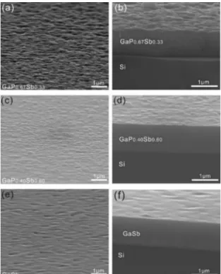
Figure 3 shows the scanning electron microscopy (SEM) images of the three GaP0.67Sb0.33/Si, GaP0.40Sb0.60/Si,
GaSb/Si samples on plane-view (Fig.3 a, c, e) and cross-section view (Fig.3 b, d, f). From these images, it can be observed that the samples GaP0.40Sb0.60/Si and GaSb/Si
exhibit relatively smooth surfaces as compared with the other sample, the GaP0.67Sb0.33/Si. The roughness observed
is attributed to both emergence of some crystal defects such
as residual dislocations and residual stress in the sample. The corresponding atomic force microscopy (AFM) images are given in the supplemental materials and the RMS (root-mean-square) roughnesses of the surfaces were found to be 22.80nm for GaP0.67Sb0.33, 9.32nm for GaP0.40Sb0.60 and
7.91nm for GaSb. It suggests an improvement of the crystal quality with increasing Sb content. This is also confirmed by a very significant Bragg peak sharpening observed on reciprocal space maps (Fig.2). Even though the GaPSb/Si samples are defective, especially for the GaP0.67Sb0.33/Si,
the high photocurrent and relatively long-lifetime stability with protecting layers measured with a GaP0.67Sb0.33/Si
photoanode for water splitting [25] indicate that carriers pass through the GaPSb/Si interface efficiently without the need of a tunnel junction, and the corrosion impact on PEC performances can be reduced effectively by protections layers [20,21,25]. Moreover, there is a large room for the improvement of the material quality, because of the specific dislocation distribution in Sb-based compounds [14,24]. The influence of localized dislocations at the III-V/Si interface on transport and screening effects will be interesting to be explored in future work.
Fig. 3. Scanning electron microscopy (SEM) images of the GaP0.67Sb0.33, GaP0.40Sb0.60, GaSb three samples on plane view (a),(c),(e) and cross-section view(b),(d),(f).
Ellipsometry measurements were made for GaPSb bandgap determination, independently of the Si substrate. Chemical mechanical polishing (CMP) was performed to obtain smoother surfaces and avoid distortion on ellipsometry measurements. The SEM plane-view images of the three CMP-polished samples are shown in Fig.S2
(supplemental materials), which shows that the surface roughnesses of the three samples are much lower than the as-grown samples. The surface RMS (root-mean-square) roughnesses of the three CMP samples extracted from AFM measurements are 0.33nm (GaP0.67Sb0.33), 0.28nm
(GaP0.40Sb0.60) and 0.56nm (GaSb), indicating the surfaces
of the three samples become very smooth after CMP processes. Then the optical constants of the three GaP0.67Sb0.33/Si, GaP0.40Sb0.60/Si, and GaSb/Si samples were
measured by variable angle spectroscopic ellipsometry (VASE) at room temperature in the 0.58–5 eV photon energy region. The angles of incidence were set to 60˚ and 70˚. A Tauc-Lorentz model with two oscillators was used to fit the ellipsometry data of the three samples (Fig.S5 in the supplemental materials). From this model, the refractive index (n), extinction coefficient (k) and absorption spectrum of the GaPSb layers of the three samples were extracted independently of the Si substrate, respectively, as shown in Fig.S6 (supplemental materials) and Fig.4 (the red curves). Besides, in order to further integrate and verify the experimental data, ellipsometry measurement was also performed on a GaP/Si sample and the corresponding optical constants extracted based on the Tauc-Lorentz model are shown in Fig.S7 (supplemental materials). The deduced absorption curves of the GaP and GaSb based on ellipsometry measurements show good agreements with both the experimental and theoretical data presented in ref. [29] (see Fig.S8 in the supplemental materials).
Fig. 4. Optical absorption spectra of the GaP0.67Sb0.33 (a), GaP0.40Sb0.60 (b), GaSb (c) semiconductors. The red lines were deduced from ellipsometry measurement and the black lines were obtained based on TB calculation.
Based on Tauc plot method, the band gap ranges of the four samples were obtained: Eg=2.25±0.04 eV for GaP; Eg=1.70±0.06 eV for GaP0.67Sb0.33; Eg=1.04±0.08 eV for
GaP0.40Sb0.60, and Eg=0.68±0.09 eV for GaSb (the details
see the supplemental materials), which are consistent with bandgaps reported for the metamorphic growth of GaPSb on InP substrate [30]. In this study, we neglect the possible impact of alloy fluctuations and Sb ordering on the bandgap determination. Further experiments would be needed to assess quantitatively the influence of such effects.
The band structures of the unstrained GaP1-xSbx alloys in
the whole Sb compositional range have then been calculated by tight-binding (TB) calculation, using an extended basis sp3d5s* tight binding Hamiltonian [31].
From the tight binding parameters of GaP and GaSb binary compounds [31], a virtual crystal approximation is performed to obtain the band structures of the different GaP1-xSbx alloys at 0K as a function of the Sb content. Then
the energies were shifted to take into account the influence of the temperature, in order to get room temperature band structures [32]. The calculated band structures of GaP, GaP0.67Sb0.33, GaP0.40Sb0.60, and GaSb semiconductors are
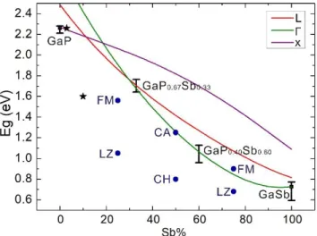
given in the Fig.S10. The bandgap evolutions obtained in the Γ, L and X valleys of the GaP1-xSbx alloy for the whole
Sb content range are presented in Fig.5, from which we can find both the band gap value and the band gap type (direct or indirect). For the GaP, GaP0.67Sb0.33, GaP0.40Sb0.60, and
GaSb semiconductors, tight-binding calculations are in good agreement with the experimental absorption measurements. The theoretical absorption curves of GaP0.67Sb0.33, GaP0.40Sb0.60, GaSb semiconductors
(corresponding to the three MBE grown samples) determined with tight-binding calculations are shown as black lines in Fig.4, which also shows good consistency with the experimental data. From this analysis, we deduce that the Sb content at which a 1.7 eV direct bandgap needed for tandem materials association obtained is 32%. Besides, the bandgap calculation of GaPSb were also investigated in previous works by density functional theory (DFT) calculations [33,34]. In these references, the bandgap values were underestimated (as compared to our TB calculation results and experimental data), which is a well- known issue with DFT calculations. Russell et al. performed DFT+U calculations [33], but this method is more adapted to transition metals and nitrides materials. Chen et al. also calculated the band gaps of different ordering structures of GaPSb based within the local-density approximation (LDA) with exchange correction function (LDA+C) [34], which compared to the general LDA results shows obvious improvement. The bandgap values reported in the literature for different ordering structures with different Sb contents are given in Fig. 5, with blue dots. It can be found that the bandgaps of the different ordering structures show obvious discrepancy. The bandgap of CA (layered tetragonal CuAu-I-like structure) with 50% Sb and FM (famatinite structure) with 75% Sb are close to our calculation data, and the CH (chalcopyrite structure) with 50% Sb and LZ (luzonite-like structure) with 25% and 75% Sb are lower than the results in the present work. Besides, the bandgaps of polycrystalline GaPSb with 3% and 10% Sb based on experimental measurement given in ref. [23] were also added in the Fig. 5, shown as the black star dots. The bandgap of polycrystalline GaP0.97Sb0.03 shows good
correspondence to the result obtained in this work, while the bandgap of GaP0.90Sb0.10 is 0.6 eV lower than the value
found in the present study, which may result from the inhomogeneity of the polycrystalline structure of the material demonstrated in ref. [23]. For the DFT calculation methods, DFT with hybrid functional and GW approximation [35] are more accurate methods for the
bandgap calculation of semiconductors and insulators, but they need high computational cost, especially for the bandgap calculation of alloyed semiconductors, such as GaPSb, which requests large structures to allow for random distribution of Sb and P atoms. Tight binding (TB) approach therefore appears as a reasonable way to achieve realistic bandgap calculation for GaPSb, and further study on band lineups.
Fig. 5. Room temperature bandgaps of GaP1-xSbx alloys with different Sb contents. The green, red and purple solid lines are theoretical curves computed by tight-binding calculations, corresponding to Γ, L and X valleys, respectively. The separated error bar lines correspond to the bandgaps determined experimentally. The black square dots correspond to the bandgaps of GaP and GaSb given in ref. [36,37]. The blue circle dots correspond to the bandgaps of GaPSb with 25%, 50%, and 75% Sb content based on DFT+C calculation obtained from ref. [34], for different ordering structures: FM (famatinite structure), LZ (luzonite-like structure), CA (layered tetragonal CuAu-I-like structure), CH (chalcopyrite structure). The black star dots correspond to the bandgaps of polycrystalline GaPSb with 3% and 10% Sb based on experimental data obtained from ref. [23].
For efficient photoelectrochemical water splitting, another important aspect is to estimate the band edge location with respect to the redox potentials of water. The band alignment (no external electric field applied) of the GaP1-xSbx/Si tandem architecture for water splitting is
presented in Fig.6 as a function of the Sb content. The VBM (valence band maximum) energy (Ev) of the GaP 1-xSbx alloy over the whole Sb content range was obtained
based on the absolute bandlineup between VBM energy of GaP and GaSb [38], which follows the linear formula Ev(GaP1-xSbx)= xEv(GaSb)+ (1-x)Ev(GaP) [39]. In a first
approximation, the evolution of the surface acidity with Sb content was neglected. The CBM (conduction band minimum) energy of the GaP1-xSbx alloy was obtained by
using the results from TB calculations presented in Fig. 5. For this alloy, the minimum of the conduction band is located in the X-valley between 0% and 11%. It then moves to the L valley for Sb contents between 11% and 30%. It finally reaches a direct bandgap configuration (minimum of
the CB in the Γ valley) beyond 30% of Sb incorporation. While the precise value predicted by the calculations for the X to L valleys crossover seems hard to confirm experimentally in this work, calculations clearly demonstrate that in any cases, an indirect to direct cross-over is expected for this alloy at around 30% Sb, contrary to previously calculated band structures using density functional theory [23]. The VBM energy of bulk GaP is very close to the oxidation potential of water, which has been verified by many reports [38,40-42]. While, in the different papers, the energy differences (between the water redox levels and GaP VBM energy) have a little difference. So, here we show the redox levels of water based on the VBM position of GaP [38] and the energy differences [38,40-42] with error bars to analyze potential water splitting reactions more accurately and comprehensively (Fig.6).
Fig. 6. Band alignment of Γ, L and X valleys of GaP1-xSbx and indirect bandgap of Si with respect to water oxidation and reduction potentials. The relative position of redox potentials of water are shown as green bars at pH=0.
From the Fig.5 and Fig.6, it can be observed first that, in order to benefit from a direct GaPSb bandgap larger than the one of the silicon (to absorb higher energy solar radiations), the Sb content should lie between 30% (indirect to direct cross-over) and 54% (bandgap equal to the Si one). In this Sb content range, it is also noticed that the band lineup is of type I, promoting the charge carrier extraction in the silicon under zero bias conditions. Now looking at the band lineups between GaPSb and the water redox potentials in the 30%-54% Sb content range, it is seen that GaPSb has a strong reduction ability due to its relatively higher CBM and it is around 0.9 eV higher than H+/ H2 potential at 32% Sb content. On the other hand, the
VBM is higher than the O2/H2O potential in the 30%-54%
Sb content range, and due to the linear increase of VBM with the Sb content, the GaPSb with low Sb content (around 30%) is thus more suitable for oxygen evolution reactions (about 0.43 and 0.46 eV higher than O2/H2O
potential at 30% and 32% Sb content). Overall, addition of
Sb in GaP will therefore ease photocathode operation, although large currents densities were obtained with a GaPSb/Si photoanode, due to a strong direct bandgap absorption in this alloy [25]. The band lineups calculated in this work thus give a basis for further devices analysis, where the precise determination of Nernstian shifts and band bending will be needed, but it is beyond the scope of this article.
4. Conclusions
In summary, the structural, electronic and optical properties of the III-V/Si-based tandem materials association GaP1-xSbx/Si for photoelectrochemical water
splitting was studied comprehensively for the whole range of Sb composition, and its potential for photoelectrochemical cell evaluated. The GaP1-xSbx alloys
were directly grown on the Si substrate with different Sb contents. The bandgap values and bandgap types of GaPSb alloys were determined on the whole Sb range, by combining the experimental data with tight binding (TB) theoretical calculations. The indirect (X-band) to direct (Γ-band) cross-over was found to occur at 30% Sb content. Especially, at a Sb content of 32%, the GaP1-xSbx alloy
reached the ideal 1.7eV direct bandgap, complementary to the Si 1.1eV one. Furthermore, the analysis of the band alignment of GaP1-xSbx alloys and Si with respect to water
potential levels shows that the GaPSb/Si association is an interesting combination both for the hydrogen evolution and oxygen evolution reactions, suggesting the GaP 1-xSbx/Si tandem material holds great promise for
high-efficiency solar water splitting on the low cost silicon substrate.
Acknowledgement
This research was supported by the French National Research Agency ANTIPODE Project (Grant No. 14-CE26-0014-01), Région Bretagne and King Abdulaziz City for Science and Technology (KACST), Riyadh, Saudi Arabia. Lipin Chen acknowledges the China Scholarship Council (CSC) for her Ph.D financial support (No. 2017-6254). Mahdi Alqahtani acknowledges the support and scholarship from King Abdulaziz City for Science and Technology, Riyadh, Saudi Arabia. The authors acknowledge RENATECH (French Network of Major Technology Centers) within Nanorennes for technological support.
References
[1] A.J. Bard, M.A. Fox, Artificial photosynthesis: solar splitting of water to hydrogen and oxygen, Acc. Chem. Res. 28 (1995) 141– 145.
[2] N.S. Lewis, D.G. Nocera, Powering the planet: Chemical
challenges in solar energy utilization, Proc. Natl. Acad. Sci. 103 (2006) 15729–15735.
[3] D. Kang, T.W. Kim, S.R. Kubota, A.C. Cardiel, H.G. Cha, K.-S.
for use in solar water splitting, Chem. Rev. 115 (2015) 12839– 12887.
[4] R. van de Krol, M. Grätzel, eds., Photoelectrochemical hydrogen
production, Springer US, 2012.
[5] J. Rongé, T. Bosserez, D. Martel, C. Nervi, L. Boarino, F.
Taulelle, G. Decher, S. Bordiga, J. A. Martens, Monolithic cells for solar fuels, Chem. Soc. Rev. 43 (2014) 7963–7981.
[6] D. Bae, B. Seger, P.C. Vesborg, O. Hansen, I. Chorkendorff,
Strategies for stable water splitting via protected photoelectrodes, Chem. Soc. Rev. 46 (2017) 1933–1954.
[7] S. Hu, C. Xiang, S. Haussener, A.D. Berger, N.S. Lewis, An
analysis of the optimal band gaps of light absorbers in integrated tandem photoelectrochemical water-splitting systems, Energy Environ. Sci. 6 (2013) 2984–2993.
[8] J.L. Young, M.A. Steiner, H. Döscher, R.M. France, J.A. Turner,
T.G. Deutsch, Direct solar-to-hydrogen conversion via inverted metamorphic multi-junction semiconductor architectures, Nat. Energy. 2 (2017) 17028.
[9] O. Khaselev, J.A. Turner, A monolithic
photovoltaic-photoelectrochemical device for hydrogen production via water splitting, Science. 280 (1998) 425–427.
[10] M.M. May, H.-J. Lewerenz, D. Lackner, F. Dimroth, T.
Hannappel, Efficient direct solar-to-hydrogen conversion by in situ interface transformation of a tandem structure, Nat. Commun. 6 (2015) 8286.
[11] W.-H. Cheng, M.H. Richter, M.M. May, J. Ohlmann, D. Lackner,
F. Dimroth, T. Hannappel, H.A. Atwater, H.-J. Lewerenz, Monolithic photoelectrochemical device for direct water splitting with 19% efficiency, ACS Energy Lett. 3 (2018) 1795–1800. [12] J.S. Ward, T. Remo, K. Horowitz, M. Woodhouse, B. Sopori, K.
Vansant, P. Basore, Techno-economic analysis of three different substrate removal and reuse strategies for III-V solar cells, Progress in Photovoltaics: Research and Applications. 24 (2016) 1284–1292.
[13] J. Tournet, Y. Lee, S.K. Karuturi, H.H. Tan, C. Jagadish, III–V semiconductor materials for solar hydrogen production: status and prospects, ACS Energy Lett. 5 (2020) 611–622.
[14] I. Lucci, S. Charbonnier, L. Pedesseau, M. Vallet, L. Cerutti, J.-B.
Rodriguez, E. Tournié, R. Bernard, A. Létoublon, N. Bertru, A. Le Corre, S. Rennesson, F. Semond, G. Patriarche, L. Largeau, P. Turban, A. Ponchet, C. Cornet, Universal description of III-V/Si epitaxial growth processes, Phys. Rev. Mater. 2 (2018) 060401.
[15] S. Chen, W. Li, J. Wu, Q. Jiang, M. Tang, S. Shutts, S.N. Elliott,
A. Sobiesierski, A.J. Seeds, I. Ross, P.M. Smowton, H. Liu, Electrically pumped continuous-wave III–V quantum dot lasers on silicon, Nat. Photonics. 10 (2016) 307–311.
[16] S. Licht, B. Wang, S. Mukerji, T. Soga, M. Umeno, H. Tributsch,
Efficient solar water splitting, exemplified by RuO2-catalyzed AlGaAs/Si photoelectrolysis, J. Phys. Chem. B. 104 (2000) 8920– 8924.
[17] P. Kumar, P. Devi, R. Jain, S.M. Shivaprasad, R.K. Sinha, G.
Zhou, R. Nötzel, Quantum dot activated indium gallium nitride on silicon as photoanode for solar hydrogen generation, Commun. Chem. 2 (2019) 4.
[18] I. Lucci, S. Charbonnier, M. Vallet, P. Turban, Y. Léger, T. Rohel,
N. Bertru, A. Létoublon, J.-B. Rodriguez, L. Cerutti, E. Tournié, A. Ponchet, G. Patriarche, L. Pedesseau, C. Cornet, A stress-free and textured GaP template on silicon for solar water splitting, Adv. Funct. Mater. 28 (2018) 1801585.
[19] A. Rolland, L. Pedesseau, J. Even, S. Almosni, C. Robert, C.
Cornet, J.M. Jancu, J. Benhlal, O. Durand, A.L. Corre, P. Rale, L. Lombez, J.-F. Guillemoles, E. Tea, S. Laribi, Design of a lattice-matched III–V–N/Si photovoltaic tandem cell monolithically integrated on silicon substrate, Opt. Quantum Electron. 46 (2014) 1397–1403.
[20] M. Alqahtani, S. Ben-Jabar, M. Ebaid, S. Sathasivam, P. Jurczak,
X. Xia, A. Alromaeh, C. Blackman, Y. Qin, B. Zhang, B.S. Ooi, H. Liu, I.P. Parkin, J. Wu, Gallium Phosphide photoanode coated
with TiO2 and CoOx for stable photoelectrochemical water
oxidation, Opt. Express. 27 (2019) A364–A371.
[21] S. Hu, M.R. Shaner, J.A. Beardslee, M. Lichterman, B.S.
Brunschwig, N.S. Lewis, Amorphous TiO2 coatings stabilize Si, GaAs, and GaP photoanodes for efficient water oxidation, Science. 344 (2014) 1005–1009.
[22] H. Döscher, O. Supplie, M.M. May, P. Sippel, C. Heine, A.G.
Muñoz, R. Eichberger, H.-J. Lewerenz, T. Hannappel, Epitaxial
III–V films and surfaces for photoelectrocatalysis,
ChemPhysChem. 13 (2012) 2899–2909.
[23] A. Martinez-Garcia, H.B. Russell, W. Paxton, S. Ravipati, S.
Calero-Barney, M. Menon, E. Richter, J. Young, T. Deutsch, M.K. Sunkara, Unassisted water splitting using a GaSbxP (1-x) photoanode, Adv. Energy Mater. (2018) 1703247.
[24] H. Nguyen-Van, A.N. Baranov, Z. Loghmari, L. Cerutti, J.-B.
Rodriguez, J. Tournet, G. Narcy, G. Boissier, G. Patriarche, M. Bahriz, E. Tournié, R. Teissier, Quantum cascade lasers grown on silicon, Sci. Rep. 8 (2018) 7206.
[25] M. Alqahtani, S. Sathasivam, L. Chen, P. Jurczak, R. Piron, C. Levallois, A. Létoublon, Y. Léger, S. Boyer-Richard, N. Bertru, J.-M. Jancu, C. Cornet, J. Wu, I.P. Parkin, Photoelectrochemical water oxidation of GaP1−xSbx with a direct band gap of 1.65 eV for full spectrum solar energy harvesting, Sustain. Energy Fuels. 3 (2019) 1720–1729.
[26] T. Quinci, J. Kuyyalil, T.N. Thanh, Y.P. Wang, S. Almosni, A.
Létoublon, T. Rohel, K. Tavernier, N. Chevalier, O. Dehaese, Defects limitation in epitaxial GaP on bistepped Si surface using UHVCVD–MBE growth cluster, J. Cryst. Growth. 380 (2013) 157–162.
[27] J.H. Kim, D. Hansora, P. Sharma, J.-W. Jang, J.S. Lee, Toward practical solar hydrogen production – an artificial photosynthetic leaf-to-farm challenge, Chem. Soc. Rev. 48 (2019) 1908–1971.
[28] T. Nguyen Thanh, C. Robert, W. Guo, A. Létoublon, C. Cornet, G.
Elias, A. Ponchet, T. Rohel, N. Bertru, A. Balocchi, Structural and optical analyses of GaP/Si and (GaAsPN/GaPN)/GaP/Si nanolayers for integrated photonics on silicon, J. Appl. Phys. 112 (2012) 053521.
[29] S. Adachi, Optical dispersion relations for GaP, GaAs, GaSb, InP,
InAs, InSb, AlxGa1−xAs, and In1−xGaxAsyP1−y, J. Appl. Phys. 66 (1989) 6030–6040.
[30] S. Loualiche, A. Le Corre, S. Salaun, J. Caulet, B. Lambert, M. Gauneau, D. Lecrosnier, B. Deveaud, GaPSb: A new ternary material for Schottky diode fabrication on InP, Appl. Phys. Lett. 59 (1991) 423–424.
[31] J.-M. Jancu, R. Scholz, F. Beltram, F. Bassani, Empirical spds* tight-binding calculation for cubic semiconductors: General method and material parameters, Phys. Rev. B. 57 (1998) 6493.
[32] Y.P. Varshni, Temperature dependence of the energy gap in
semiconductors, Physica. 34 (1967) 149–154.
[33] H.B. Russell, A.N. Andriotis, M. Menon, J.B. Jasinski, A.
Martinez-Garcia, M.K. Sunkara, Direct band gap gallium antimony phosphide (GaSb x P 1- x) alloys, Scientific Reports. 6 (2016) 20822.
[34] D. Chen, N.M. Ravindra, Structural, thermodynamic and
electronic properties of GaPxSb1–x and InPxSb1–x alloys, Emerging Materials Research. 2 (2013) 109–113.
[35] W. Chen, A. Pasquarello, Band-edge levels in semiconductors and
insulators: Hybrid density functional theory versus many-body perturbation theory, Phys. Rev. B. 86 (2012) 035134.
[36] M.B. Panish, H.C. Casey, Temperature dependence of the energy
gap in GaAs and GaP, J. Appl. Phys. 40 (1969) 163–167.
[37] M. Wu, C. Chen, Photoluminescence of high-quality GaSb grown
from Ga- and Sb-rich solutions by liquid-phase epitaxy, J. Appl. Phys. 72 (1992) 4275–4280.
[38] C.G. Van de Walle, J. Neugebauer, Universal alignment of
hydrogen levels in semiconductors, insulators and solutions, Nature. 423 (2003) 626.
[39] B.M. Borg, L.-E. Wernersson, Synthesis and properties of
antimonide nanowires, Nanotechnology. 24 (2013) 202001. [40] D. Jing, L. Guo, L. Zhao, X. Zhang, H. Liu, M. Li, S. Shen, G.
photocatalytic water splitting: from fundamental study to pilot demonstration, Int. J. Hydrog. Energy. 35 (2010) 7087–7097.
[41] S. Chu, W. Li, Y. Yan, T. Hamann, I. Shih, D. Wang, Z. Mi,
Roadmap on solar water splitting: current status and future prospects, Nano Futur. 1 (2017) 022001.
[42] A. Kudo, Y. Miseki, Heterogeneous photocatalyst materials for