Design of the Configuration and Diagnostic
Units of the MAP Chip
by
Keith Klayman
Submitted to the Department of Electrical Engineering and
Computer Science
in partial fulfillment of the requirements for the degree of
Master of Science in Computer Science and Engineering
at the
MASSACHUSETTS INSTITUTE OF TECHNOLOGY
May 1997
@ Massachusetts Institute of Technology 1997
All rights reserved.
A uthor .
...
Department of Electrical Engineering and Computer Science
May 27, 1997
A ,cc=Certified by
Accepted by.
L...
William J. Dally
Professor
Thesis Supervisor
Arthur C. Smith
Chairman, Department Committee on Graduate Students
BARKER
Design of the Configuration and Diagnostic
Units of the MAP Chip
by
Keith Klayman
Submitted to the Department of Electrical Engineering and Computer Science on May 27, 1997, in partial fulfillment of the
requirements for the degree of
Master of Science in Computer Science and Engineering
Abstract
This thesis presents the design of the Configuration and Diagnostic units of the MAP chip. The MAP chip is a new microprocessor being developed for the M-Machine project. The Configuration units allow for the storage and access to various counters, thread state, and cluster data needed for thread swap. The diagnostics unit is re-sponsible for booting the processor and is used as the interface between the external pins and the DIP and SCAN chains.
Thesis Supervisor: William J. Dally Title: Professor
Acknowledgments
There are many people without whom this thesis would not be possible. First of all, I would like to thank Professor Bill Dally for giving me the opportunity to work in his group. The past year has been the most grueling but most rewarding time for me at MIT. I learned so much by working on this real world type project. Many thanks go to Steve Keckler and Andrew Chang for being so patient with me and all of my questions. Also, thank you to Nick Carter for the documentation on the Memory System Config, Albert Ma for his work on the I/O subsystem and Whay Lee for all his help with the switches.
Finally, I would like to thank my family. Without their support I could have never made it to MIT. I could never give you all the credit you deserve, but here is a little.
Contents
1 Introduction 8
1.1 Architectural Overview ... 8
1.2 Switches . . . ... . . 10
1.3 Global Configuration Unit ... 11
1.4 Diagnostic Unit ... 11
1.5 Thesis Outline . .. ... ... .. .. .... 12
2 Global Configuration Unit 13 2.1 Overview .. .. .. .. ... .. ... .. 13
2.2 Addressing ... ... . ... ... 16
2.2.1 LCFG . . . . 16
2.2.2 Global State ... ... ... .. ... .... 18
2.2.3 CSW Transactions and Network State . ... 19
2.2.4 I/O Addressing ... 20
2.2.5 Memory System Configuration Space Addressing ... . 20
2.2.6 Performance Monitoring ... .. 21
2.3 Global Configuration Space Control . ... 22
2.3.1 GCFG State Machine ... 22
2.3.2 MSW and CSW interface ... 23
2.3.3 Decode and Global State ... 23
2.3.4 I/O subsystem ... 24
3 Putting it all Together: Playing with Threads 3.1 Starting a New Thread . ...
3.2 Thread Swap ...
3.2.1 Thread Evict . . . . 3.2.2 Thread Install . ...
4 Diagnostic Unit
4.1 Introduction ...
4.2 High Level Design and Interface ...
4.2.1 Interface . ... . 4.2.2 Functions ... 4.3 MSW Module ... 4.4 CSW Module ... 4.5 SCAN chain ... 4.6 DIP chain . .. .. .. .. ... .. .. .. ... 4.7 Boot Sequence for the MAP Chip ... 5 Conclusions
5.1 Sum m ary . . . . 5.2 Suggestions For Improvement ...
A Event System
B Programmers guide to Config Addressing C Routines used in Thread Swap
28 28 31 31 32 34 34 35 35 36 37 40 41 43 44 46 46 47 48 57
List of Figures
1-1 The MAP chip ...
1-2 Relationship of V-Threads to H-Threads . 2-1 2-2 2-3 2-4 2-5 2-6 2-7 2-8 4-1 4-2 4-3 4-4 4-5 4-6 4-7 4-8 4-9 GCFG Block Diagram ...
Configuration space address bits . . . . . .
Partition of CSW Packet to LCFG . . . . . Partition of Generic CSW Control Packet
I/O Address fields ...
GCFG State Machine diagram . . . . Timing from M-Switch to C-Switch in GCFG MSW to CSW timing with late_kill . . . . .
Block diagram of the DIAG . . . . Timing diagram for setting reset . . . . Schematic of diag_cmd registers . . . .
Timing diagram for off chip MSW read . . .
Timing of the CSW registers . . . . Timing diagram for off chip CSW read . . . Schematic of PDFFSCAN register . . . . . SCAN chain timing ...
DIP chain timing ...
. . . . 15 S . . . . . . 16 S . . . . . . 18 S . . . . . . 20 . . . . 20 S . . . . . . 22 S . . . . . . 26 S . . . . . . 27
Chapter 1
Introduction
The M-Machine is an experimental multicomputer developed by the Concurrent VLSI Architecture Group in the Artificial Intelligence Lab at the Massachusetts Institute of Technology. As a member of the group, I participated in many facets of the project. My main contributions were made in the design and implementation of the Configuration and Diagnostic units. Work was also done to test these components at the behavioral level. This thesis presents the design of these units and discusses how the Configuration and Diagnostic units will be used when the MAP chip returns from fabrication.
1.1
Architectural Overview
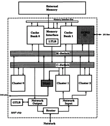
The M-Machine consists of a collection of computing nodes interconnected by a bidi-rectional 2-D mesh network. Each node will consists of a multi-ALU (MAP) chip and 8 MBytes of synchronous DRAM [2]. The MAP chip includes a network interface and router which provide low latency communication in the X and Y directions. A dedicated I/O bus is also available on each node.
As shown in figure 1-1, a MAP contains: three execution clusters, a memory subsystem comprised of two cache banks and an external memory interface, and a communication subsystem consisting of the network interfaces and the router. Two crossbar switches interconnect these components.
O1 Bus
DIAG
Figure 1-1: The MAP chip
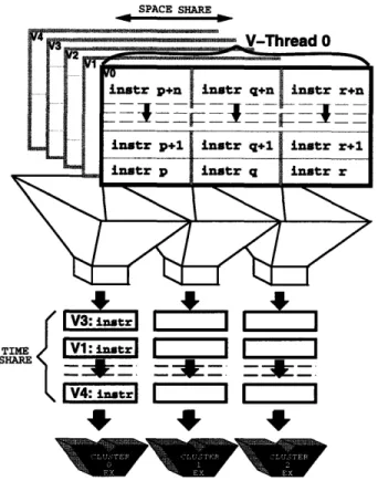
The M-Machine provides hardware that allows many threads to run concurrently on a node. There are enough resources for five V-Threads, each of which consists of three H-Threads, one H-Thread per cluster. Two of the five V-Threads are user threads, while the other three are for handling exceptions, events and the system runtime software. H-Threads can communicate through registers, with each having the capability to write values to the register files of the other H-Threads within the same V-Thread. The H-Threads in a V-Thread can execute as independent threads with different control flows for exploiting loop or thread-level parallelism. On the other hand, the H-Threads can be scheduled statically as a unit to exploit instruction level parallelism, as in a VLIW machine. The V-Threads are interleaved at run-time over the clusters on each cycle. See Figure 1-2 for an illustration of the relationship between V-Threads and H-Threads.
SPACE SHARE
---
V-Thread 0instr p+n instr q+n instr r+n
instr p+1 instr q+1 instr r+l instr p instr q instr r
V1: instr
I
V4 : inttrlI
II
I
4
!I,
Figure 1-2: Relationship of V-Threads to H-Threads
1.2
Switches
The two crossbar switches provide single cycle latency communication between all units of the MAP chip. The M-Switch (MSW) provides a means for the clusters to request data and instructions from the memory system [5]. The C-Switch (CSW) is used by the memory system and queues to write to any cluster. In addition, the CSW provides a path between the clusters [6].
The switches also accommodate the configuration and diagnostic units. Both units require the ability to read and modify distributed pieces of state throughout the MAP chip. The switches provide efficient access to this state that reduces the wiring required in alternative solutions. The Global configuration unit looks much like a cache bank to the switches. It consumes data from the MSW and produces over the CSW. The Diagnostic unit requires the ability to send over the MSW and
listens on the CSW output port of Cluster 1.
1.3
Global Configuration Unit
A Global Configuration Unit is necessary to facilitate the management of hardware
located throughout the MAP chip. A central unit is required due to the thread
architecture of the MAP. It is expected that a single thread will act as the run time
system, it is essential that this thread have the ability to access all state throughout
the MAP.
Expected primary uses of the Global Config include thread swap, performance
metering, filling registers on software handled loads, I/O, LTLB and Network access. By controlling these functions from a central location and sharing the switch interfaces we do not waste routing resources. In addition, we conveniently use the load and store operations to address the Configuration address space. This enables the run time system to efficiently access the hardware.
1.4
Diagnostic Unit
The MAP diagnostic unit is required for two reasons:
1. System initialization and reset (warm and cold resets). This includes: * Whole chip reset - ie. clearing, queues etc..
* Setting "DIP" switches
* Initializing off chip memory
* Loading boot strap program into memory 2. Ability to test control and data functionality.
This implies that all control NLTCH and PDFF cells can be isolated and tested for functionality. The main purpose of this level of testing is to ensure logic works as designed.
The verification function of the diagnostic system is based on the following assumptions:
* The diagnostic system will be employed to isolate logic errors so that they may be more fully explored in the RTL simulator.
* The diagnostic system will not be used to detect and isolate manufacturing bugs (ie. shorts, opens).
* Application program debug will be performed via breakpoints (implies ability to access data without effecting threads.)
1.5
Thesis Outline
This thesis will overview the design of the Configuration and Diagnostic units. This will include trade-offs made throughout the design and the information needed to design an interface. The next chapter will detail the Global Configuration unit. Following that chapter will be a discussion of the requirements for thread swap on the MAP chip. Then a chapter on the design of the Diagnostic unit. This chapter will include a detailed description of the timing and steps required to boot the MAP chip. The final chapter serves as the conclusion to this thesis. Appendix A provides a reference for Event addressing while Appendix B does the same for composing GCFG addresses. Appendix C provides sample code used by the runtime system for thread swap.
Chapter 2
Global Configuration Unit
2.1
Overview
The configuration space controller is divided into several pieces and is distributed throughout the MAP. A global configuration space controller (GCFG) resides in a central location. It receives all configuration space requests via the M-Switch and either takes the appropriate action or forwards the request to a local configuration space controller. A local configuration space controller (LCFG) resides within each cluster. It is responsible for all state modifications within that cluster. Requests are sent from the GCFG to the LCFG via the C-Switch (CSW).
The GCFG shares an M-Switch data port with Cache bank one and has it's own ready and data available signals. When the GCFG receives data from the MSW it decodes the request based on the address provided, and does one of the following:
* Write a piece of state located in the GCFG
* Read a piece of state located in the GCFG, returning value across the CSW * Forwards the request to a cluster configuration space controller via the CSW * Generates a generic CSW command
* Access the I/O controller
The various components of the GCFG are accessed by an extremely large address space that is sparsely populated by physical resources. The GCFG decode module uses the address from and MSW packet to target the destination of the request.
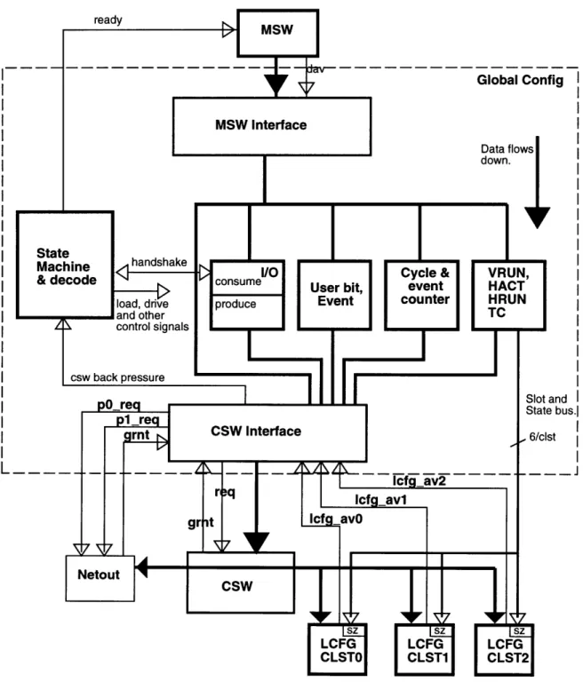
The GCFG contains a top wrapper that includes a state machine and decode module along with five major modules that manipulate data: MSW interface, CSW interface, Counters (cycle and event), I/O and GCFG state registers (HACT, HRUN, VRUN, TC, User, Event). Figure 2-1 shows the block diagram of the GCFG. Data flows from the MSW and either writes to the various modules or reads a value and is held in the CSW module until arbitration is won.
The MSW module contains a set of recirculating PDFF cells that load when empty and the MSW asserts the data available signal. Data is held in the PDFF's until it is consumed by the CSW or terminates in the other modules. The CSW interface performs the multiplexing of the data and arbitrates with the CSW, netout and LCFG. The data packet is held in a recirculating NLTCH while arbitrating for the CSW. The cycle and event counters, 64 and 32 bits respectively, are implemented in eight bit chunks with a fast carry. The I/O module consumes data from the MSW interface and produces to the CSW an arbitrary time later.
Figure 2-1: GCFG Block Diagram ready fig ndI Sbus.l t L.
2.2
Addressing
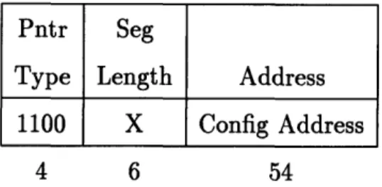
The Configuration Space is accessed by software loads and stores to pointers tagged with the configspace type as shown below.
Pntr Seg
Type Length Address 1100 X Config Address
4 6 54
The large address space of the Configuration unit allows the hardware to quickly decode which partition to send a request. These partitions are encoded in a one-hot fashion at the top of a Config address as shown in Figure 2-2.
~mem csw
gbl cist I/O
other
address
X
1
1
1
1
1
22
24
3
Figure 2-2: Configuration space address bits.
The five bits (-mem, csw, global, clst, i/o) identify where the access must be serviced within the global configuration space controller. If the mem bit is set to zero then the access is intended for the Memory System. These transactions are sent over the M-Switch and through the bank without disturbing the GCFG. Only one of the other four bits should be active in any GCFG address. The address field identifies a piece of hardware for the selected destination of the access.
2.2.1
LCFG
LCFG state is addressable by setting the clst bit at the top of the address field. LCFG addresses will consist only of the low 11 bits of the address field. The top two bits of this 11 bit field will specify the relative cluster. When accessing Local state that is duplicated for each Vthread the next three bits will specify the thread and
Table 2.1: LT offsets
Thread Slot Data LC offset Access Mode LCFG NOP 0x1D8 Write Only Exception bit OxIFO Read/Clear Catastrophic Exception Bit 0x1F8 Read
Table 2.2: LC offsets
the low six bits will specify the offset as shown in Table 2.1. The low six bits, LT offset, target a specific piece of state within a thread. The per Cluster LCFG state is addressable by the 9 bit address given in Table 2.2. These addresses, LC offset, target the exception information and thread independent NOP.
Below is the format for accesses to the per thread state. 11 0 1 0 X cid tid LT offset X
1 1 1 1 1 35 2 3 6 3 Below is the format for accesses to the cluster state.
I1 0 10 1 10 1 X I cid 1111 1 LC offset IX 1 1 1 1 1 35 2
Thread Slot Data LT offset Access Mode Integer Registers OxO - 0x78 Read/Write FP Registers 0x80 - OxF8 Read/Write HThread IPs Mapped into GPRs Read/Write CC Registers Ox100 - 0x138 Read/Write CC Registers at once 0x140 Read Only MEMBAR Counter 0x148 Read/Write
HThread Init 0x150 Write Only
HThread Priority 0x158 Read/Write Preempt/Stall Counter 0x160 Read/Clear Preempt Threshold Register 0x168 Read/Write Stall Cycle Bit 0x178 Read/Clear Integer Scoreboard 0x188 Read/Write FP Scoreboard 0x190 Read/Write CC Scoreboard 0x198 Read/Write Thread Restart IP Write OxlA0 Write Only
HFork IP 0x1A8 Write Only
Thread Restart IP Read Ox1B0 Read Only Branch Pending bit Ox1CO Read Only
Reading Cluster State
Reads to state located in the cluster are forwarded to the LCFG via the CSW. This request includes the address of the state to read, as well as the name of the destination register (the LSB of the register ID is place in the MEM Sync bit). Refer to figure 2-3 for the organization of the CSW packet sent to the LCFG.
Writing Special Registers
Like reading state, writing register requests are forwarded to the LCFG. The GCFG sends a command of the same format to the LCFG with the 'Load Destination' field unused.
Writing General Registers
General registers are written directly from the GCFG across the CSW without inter-vention from the LCFG. Both data and CC registers are written directly.
Handshake Load Destination Address Data
Reg LCFG Mem
dav hld rf [3:1] clstid slotid Tslot Store slot Addr sync Data word
1 1 1 3 2 3 3 1 3 6 1 65 bits
MSB
I I II LSB
LSB
Figure 2-3: Partition of CSW Packet to LCFG
2.2.2
Global State
Global state is addressable by setting the gbl bit at the top of the address field. The state is then accessible by setting the offset to that given in Table 2.3. TC Mode, VThread run, HThread run and HThread active each have six addressable locations, one per thread. These six locations are addressable by using the low six bits of the address as a one-hot field specifying the desired thread. Each VThread run and TC Mode location are one bit, the HThread Run and HThread Active are 3 bits wide
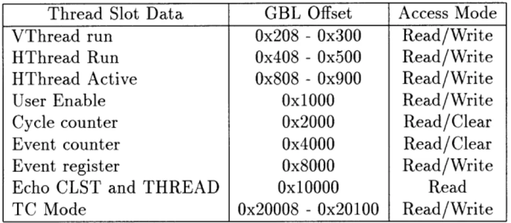
Thread Slot Data GBL Offset Access Mode VThread run 0x208 - 0x300 Read/Write HThread Run 0x408 - 0x500 Read/Write HThread Active 0x808 - 0x900 Read/Write User Enable Ox1O00 Read/Write Cycle counter 0x2000 Read/Clear Event counter 0x4000 Read/Clear Event register 0x8000 Read/Write Echo CLST and THREAD Ox1O000 Read TC Mode 0x20008 -0x20100 Read/Write
Table 2.3: Global state offsets (Local access).
(one bit per cluster.) User Enable is one bit and Event Register is seven bits. A write to the cycle (64 bits) and event (32 bits) counters will clear them. When echoing the CLST and THRD ID they will be returned in the low five bits of the result respectively.
Below is the format for accesses to the global state. 1 0 1 0 0 X GBL offset X 1 1 1 1 1 32 14 3
2.2.3
CSW Transactions and Network State
CSW transactions are generated by setting the csw bit at the top of the address field. The low 22 bits are placed directly into the 22 bits of CSW control and the next two bits are the cluster destination. The Network state is accessible by generating the correct CSW transaction. The GCFG recognizes the destination is the NETOUT unit and requests access to the NETOUT in addition to the CSW bus [4].
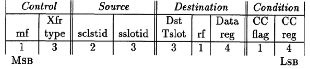
Below is the format for generating generic CSW transactions. The structure of a generic CSW packet is shown in figure 2-4.
1 0 0 0 X 1 dst cid CSW control X 1 1 1 1 1 22 2 22 3
Control Source Destination Condition
Xfr Dst Data CC CC
mf type sclstid sslotid Tslot rf reg flag reg
1
3
2
3
3
1
4
1
4
MSB LSB
Figure 2-4: Partition of Generic CSW Control Packet
2.2.4
I/O Addressing
Figure 2-5 shows the structure of I/O transactions. Two bits encode the address length in packets, and 2 bits encode the data length in packets. An address length of 2'bll indicates a burst load or store [7].
Address Length
Data Length
/
11xx Isegment
Length
110001
I10 Address 000
63 60 59 54 53 49 48 47 46 45 44 3 2 0
Figure 2-5: I/O Address fields
2.2.5
Memory System Configuration Space Addressing
The memory system's configuration space state is accessed through config space point-ers which have their high bit set to zero, which causes the M-Switch to route requests based on these pointers to the memory system to be handled. The configuration space state in the memory system consists of the contents of the LTLB, which may be read and written, and four write-only registers which control the locking of the ltlb during an LTLB miss, the error correction code (ECC) circuitry, and whether or not blocks in the cache are marked invalid on a block status miss. Attempts to read the write-only registers have unspecified results. Table 2.4 shows the addresses allocated to each of these regions. Note that these address values include the high 10
bits of the pointer, which indicates that the pointer refers to configuration space. As shown, the memory system ignores bits 28-59 of configuration space addresses when determining which piece of state is being accessed.
Memory State Address Access
LTLB OxC00000000000000-0xCO0000000OOFFFFF8 MSW (r/w) Clear Lock OxC000000001000000 MSW (write) Discard Req OxC000000002000000 MSW (write) ECC Control OxC000000004000000 MSW (write) Inv. on Miss OxC000000008000000 MSW (write)
Table 2.4: Memory system configuration space address allocation
2.2.6
Performance Monitoring
Performance monitoring uses the event register and event counter. The event register
(7 bits) selects a particular event type. These seven wires are run to all event gener-ating sites. A single bit runs through the event genergener-ating sites through a mux and PDFF at each site. This bit enters the GCFG as event_inc and the event counter is incremented for every cycle it is high. The event register is read and writable while the event counter can be read and is cleared on a write. For a list of the events and their addresses refer to appendix A.
This distributed system is quite simple, but is not without it's problems. Specif-ically, it is not possible to get a precise count of an event. There will always be on the order of 10 cycles at the beginning and end of your count which you will not have control of. This is acceptable since the expected use of the event system will be over extremely long stretches of code.
Reset
-CSW -msw.
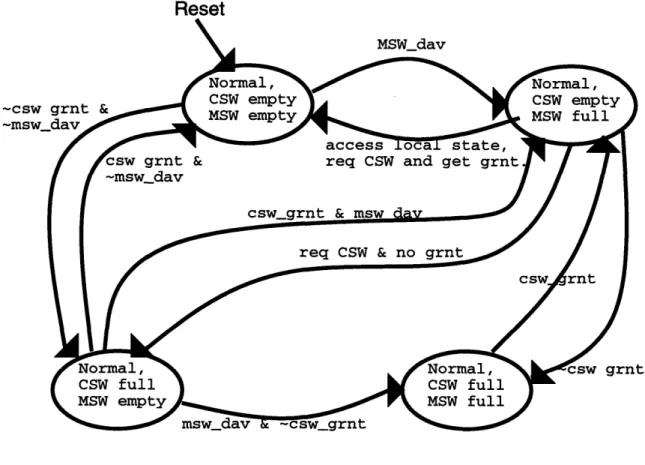
Figure 2-6: GCFG State Machine diagram
2.3
Global Configuration Space Control
2.3.1
GCFG State Machine
The GCFG is designed to minimize the back pressure placed on the MSW during high usage periods and provide minimal latency for infrequent usage. Minimal back pressure on the MSW is desirable for two reason: this pressure could cause threads in the cluster to stall and it can allow I/O access while waiting on the CSW.
With this in mind the GCFG is pipelined to hold two accesses. When a request is pulled off of the MSW it is held in a set of recirculating PDFF's. When it is necessary to send data out via the CSW the packet is formed and subsequently held in a set of recirculating NLTCH's. The four combinations of these two states being full or empty provide the first four states of the state machine shown in Figure 2-6.
out of order. This can occur when the first request is waiting for a CSW grant when a second request enters from the MSW and updates state within the GCFG. In most cases this is acceptable behavior. However, it can be avoided by sending a Configspace write to a register IO. This ensures that all requests before register write will leave the GCFG before any following requests update state.
2.3.2
MSW and CSW interface
The MSW interface is simply a recirculating PDFF with a load based on current and next state. If the PDFF's are currently empty or will be empty on the next state they are loaded. The CSW interface on the other hand requires two levels of muxing and additional logic for the csw.req signal.
The first level of muxes in the CSW interface compiles the packet from the GCFG. The second level takes that packet, I/O packet and the recirculation path to feed the NLTCH's that drive to the CSW.
The request logic is responsible for conforming to the normal CSW timing and also requesting the NETOUT unit or LCFG when appropriate. In order to reduce delay, a normal CSW operation is assumed, in the case where the destination is not available but the CSW is granted, latelkill signal is used to send an abort packet. The latekill can be used when the available signal from the LCFG (1cfg_av) is not high or the netout unit does not grant.
2.3.3
Decode and Global State
The decode in the GCFG enables the various write signals and muxes. It decodes the command and address in the MSW PDFF registers and asserts the correct signals to write or read local state. These signals will be held until the data leaves the MSW registers.
The accessible state residing within the cluster controller is listed in Table 2.3. Most state is held in PDFF's and is read through a series of muxes that lead to the CSW interface.
The HACT, HRUN, VRUN and TC data are held in NDFF's and thus have a redundant pitch in the path. However, this is necessary to satisfy the timing to the cluster. All writes to these bits must be conveyed to the cluster SZ stages. This is facilitated by a three bit thread ID and a two bit state bus between the GCFG and each cluster. The thread ID will be set to 3'blll in the idle case. When it identifies a thread, the top bit of state will specify whether TC Mode should be active and the low bit of state is one if HRUN, HACT and VRUN are all one. This transaction occurs on the second half of the cycle.
2.3.4
I/O subsystem
In addition to the normal flow of data, the I/O subsystem can consume data from the PDFF's off the MSW and provide data for the NLTCH's out to the CSW. A handshaking protocol for both of these exchanges has been implemented. Whenever the NLTCH's in the CSW interface are available, the I/O has priority over GCFG data.
2.4
Timing
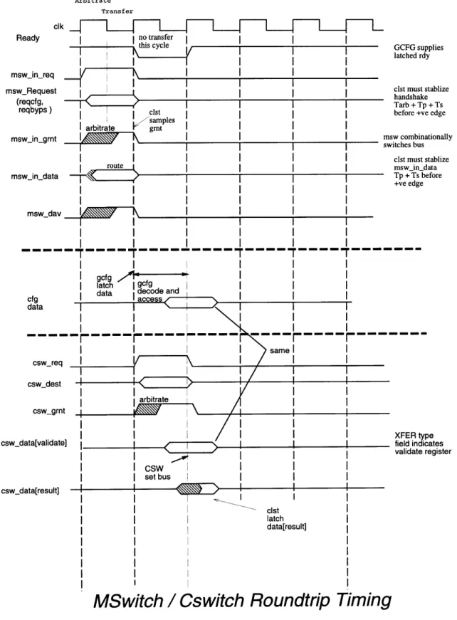
Figure 2-7 shows the round trip timing from M-Switch to C-Switch through the GCFG. The GCFG is constrained by the requirements of the MSW and CSW. It must read data from the MSW with an NLTCH and drive data to the CSW with an NLTCH. The PLTCH required to complete the path is added to the input NLTCH to form a PDFF. This leaves a full cycle (minus setup time for an NLTCH) from the
PDFF load until data must be ready for the NLTCH.
The top half of figure 2-7 shows the GCFG interaction with the MSW arbiter. Ready is provided by the GCFG to the MSW, msw_dav is is an input to the GCFG from the MSW, and msw_in_data is driven on the MSW bus to the GCFG. The lower half of the figure shows that cswreq and cswAdst are derived quickly inside the
GCFG and sent to the CSW arbiter.
When a request comes in from the M-Switch, the decoder quickly determines if the C-Switch is required and immediately begins arbitration for it. The data from global state reads is delivered across the C-Switch on the subsequent cycle or when arbitration is won. The input and output latches allow the next request to enter the GCFG even if C-Switch arbitration is lost.
In the event CSW arbitration is won, however the NETOUT or LCFG resource is not available, an abort packet is sent while the data remains in the CSW inter-face module. Arbitration for the CSW is suspended until the resource is available. Figure 2-8 shows the case when latekill causes an abort packet to be sent and CSW arbitration to wait one cycle.
Arbitrate Transfer clk Ready msw in re rns Ii no transfer I I a \I nsw_nequest (reqcfg, reqbyps ) clsts samples arbitrate grt mswin.grnt I mswindata I I GCFG supplies latched rdy clst must stablize handshake Tarb + Tp + Ts before +ve edge msw combinationally switches bus clst must stablize msw in data Tp + Ts before +ve edge msw_dav I. I I I I I I I I I I I I -~~~rf f(---I I I I I ,, fA - I II Iatc gcfg
data decode and
cfg acces s data II I II csw_req cswdest csw_grnt csw_data[validate] csw_data[result] XFER type field indicates validate register I csw I I I set bus I I clst latch data[result]
MSwitch / Cswitch
Roundtrip Timing
Figure 2-7: Timing from M-Switch to C-Switch in GCFG.
my
-• I
__ • ... =
Arbitrate Transfer clk Ready no transfer I I this cycle mswinreq nsw_Request (reqcfg, reqbyps) clst samples I arbitrate grnt msw_ingrnt 1& I I I I GCFG supplies latched rdy clst must stablize handshake Tarb + Tp + Ts before +ve edge msw combinationally switches bus clst must stablize msw in data Tp + Ts before +ve edge mswindaroute msw in data I I I I I I I I I I I I I I I I I I I I I I I I gcfgo 1 I I I latch gcfg I data decode and
fg I I xp
Data held 'in
CSW NLTCH I
I I I I I I
csw req
csw dest
csw n Iarbitrate
late kill: due to netout arb lost or Icfg not avail
csw_data[validate] csw_data[result] ta I I Sen I I SIo I III CSW set bus I I I I"lath cist I latch data[result] I
MSwitch
/
Cswitch
Roundtrip Timing
Figure 2-8: MSW to CSW timing with latelill
rI XFER type field indicates validate register
s
-- ~-I I I IIIF
11
Chapter 3
Putting it all Together: Playing
with Threads
At this point, all the facilities needed to start and swap a thread are available. We have the ability to turn threads on and off, read and write thread state, and manipulate the IP's. There are two mechanisms for starting a new thread. The first, HFORK, is available to all users but is limited in functionality [3]. The second, referred to as VFORK, requires more steps but it allows the destination to be any of the 15 VThreads. Finally, the steps required to remove an active thread and install it at a later time in any thread are discussed in the second section.
3.1
Starting a New Thread
HFORK The HFORK instruction allows any user thread to start a new HTHREAD on a neighboring Cluster. The HFORK command is limited in that the new HTHREAD will always fall within the same VTHREAD as the parent. The HFORK command is robust in that it does not allow the overwriting of active threads. It accomplishes this by first checking the HThread Active bit for the destination thread. In the case where there is an active thread the GCFG will return a CC value of zero and is done. When the HFORK is allowed to complete the GCFG state machine sequences through a series of steps that target the destination Thread with the following actions:
* Write the new IP and set HThread Active * Send the LCFG Hinit
* Send an LCFG NOP
* Return the CC value and set Hthread Run
The LCFG NOP is required to ensure the IP advances to the top of the pipeline before the thread is activated by turning on HThread Run. This new thread can complete by executing an HEXIT command, this will clear the HThread Active and run bits. Below is a code segment that will FORK a new process one relative HThread to the right: instr ialu _pointl: instr ialu instr ialu instr memu instr ialu
imm (_hfork_dest - _pointl), i7; lea ii, i7, i7;
mov #1, i6;
hfork i7, i6, ccl; cf ccl br _hfork_fail;
_hforkdest:
instr memu hexit; --spin:
instr ialu br __spin;
instr ialu add iO, iO, iO; instr ialu add iO, iO, iO; instr ialu add iO, iO, iO;
VFORK The second mechanism leaves each of these steps to the master thread.
the address. In order to ensure that the IP is loaded in the IFU, two instructions should go through the GCFG to the destination LCFG before the thread is activated. The following example show the sequence of instructions to execute a VFORK onto Cluster 1, VThread 1 from anywhere assuming:
= OxF424000000000fd8 = Oxc028000000000210 = Oxc028000000000410 = Oxc028000000000810 Oxla8 = Ox150 = OxF424000000001200 /* CFGLCFGNOP */ /* VIVRUN */ /* VIHRUN */ /* ViHACT */ /* CFGLTHFORKIP */ /* CFGLTHINIT */
/* CFGBASELC for CLST 1 SLOT i*/
/* i4, i5, i6 and i8 have pointer bit set*/
instr ialu imm (_vforkdest - _pointl), ill; _pointl:
instr ialu lea il, ill, ill;
instr
instr
instr
instr
memu Id i6, i10;
ialu and i10, #2, i12; /* ialu ine i12, iO, ccO; /* ialu ct ccO _vforkfail;
instr ialu lea i8, i7, i9; instr memu st ill, i9; instr ialu lea i8, i15, ii instr memu st iO, i15; instr memu Id i5, i13; instr ialu or i13, #2
memu st iO, i3; instr memu st i13, i5
ialu mov #1, i14; instr memu st i14, i4;
instr instr
ialu or i10, #2, ilO; memu st i10, i6;
5; /*
5; /,
/*
/*
Is there a thread active already */ in cluster 1 */
Create Pointer to write IP */
Write the IP */
Make the HINIT pointer */ Assert HINIT */
Get the HRUN 3bit vector */
/*
Send LCFG NOP */
/* Send new HRUN vect */
/* Assert the VRUN bit */
/* i10 still has HACT vector */
/* St the new HACT with CLST1 Active */
i3 i4 i5 i6 i7 i15 i8
3.2
Thread Swap
The Configuration Space controller provides the ability to read the state of a thread and store it in memory for a period of time before installing it. The runtime system for the M-Machine is to be coded in the C programming language. The following structure is to be used to store thread state:
struct HContext { int intregfile[16]; int fp_reg_filee[16]; int cc[8]; int cc_all; int hardwarembarcounter; int restartIPvector [4]; int intemptyscoreboard; int fpemptyscoreboard; int ccemptyscoreboard; int bp; int stall_bit; int priority; int PC; int PT; /* 16 integer registers /* 16 floating-point registers /* cc registers
/* all 8 cc registers at once /* hardware memory-barrier counter /* IP's to restart the thread /* register empty-state scoreboard
/* register empty-state scoreboard
/* register empty-state scoreboard /* Branch pending bit */
/* Stall cycle bit */
/* Hthread priority */
/*preempt counter*/ /*preempt threshold*/
3.2.1
Thread Evict
When reading out the thread state it is necessary to check that the Memory Barrier Counter, MEMBAR_CTR, is zero. This ensures there are no outstanding memory requests. After this check is complete the state can be read. The only state of interest when reading is the Restart IP. It is read four times to obtain all four IP's in the pipeline, in addition, it should be noted that this read is destructive. Due to area limitations on the MAP chip, the floating point units were removed from Clusters 1 and 2. This is resolved in the thread swap code by a conditional statement surrounding all reads and writes to FP state:
/* Set CP to address of Floating Point Register Zero */
if(ht == 0)
for (i = 1; i < 16; i++) { hc->fpregfile[i] = CP [i];
/* When CP address is Floating Point Scoreboard */
if(ht == 0)
hc->fpemptyscoreboard = CP[0];
For the full subroutine used to swap a thread context out see Appendix C.
3.2.2
Thread Install
The code sequence used to install a thread is much the same, however, there are two peculiarities of the Configuration Unit that require special attention. The first involves writing the three scoreboards. The second is due do the way in which IP's are loaded.
Scoreboard Write The three scoreboards, integer, floating point and CC, are implemented in identical fashions. In each case, relatively large amounts of routing resources and nontrivial control logic would be needed to implement a familiar parallel load. To avoid this, a write to a scoreboard via Config space is a two stage process. While the Config request is in the RR stage of the pipeline all scoreboard bits are set to valid. Thus, by requiring the data vector written to the scoreboard to have ones in locations the scoreboard should get zeroes, we have reduced the problem to an empty instruction. This is exactly what occurs, the RR stage of the LCFG creates a modified empty instruction and sends it down the pipeline. To save routing resources, the 16 bit vector should be shifted left 48 bits. Add the inversion detailed above and you have the vector needed. Below is a code segment that writes the three scoreboards assuming CP is a pointer the the address of the integer scoreboard of the destination thread:
CP[0] = 1 - (hc->int-emptyscoreboard << 48); if(ht == 0)
CP[1] = 1 - (hc->fpemptyscoreboard << 48);
CP[2] = 1 - (hc->ccemptyscoreboard << 48);
IP Write Both the state of the BP bits and the integer unit operation referenced by the first TRIP (ipv2) must be examined to determine how to properly restore the thread state when installing a thread. If the IU operation referenced by ipv2 was a branch or a jump, then a configuration space store to HTAHFORKIP should be used to properly setup the pipeline IP's. If the IU operation was not a branch or a jump, then four successive configuration space stores to HT_TRESTART_W should be used to install the IP's. If the Branch Pending bit for the selected thread was asserted then all four of the IP's that were read out and saved are valid and should be re-installed. If the BP bit was not asserted then the last IP (fip_2) previously saved is NOT valid. The fourth IP required for TRIP load should be generated by incrementing the third IP (if _iip_2) by 4, 8, or 12, based on the length of the instruction. Here is the code segment to accomplish this (the functions called are assembly routines provided in Appendix C): if (isbranch(hc->restartIPvector[O])) HTHFORKIP = hc->restartIPvector[O]; else
{
HTTRESTART_W = hc->restartIPvector[O]; HTTRESTART_W = hc->restartIPvector [21] ; HTTRESTARTW = hc->restartlPvector[2]; if (hc->bp) HTTRESTART_W = hc->restartIPvector[3]; elseChapter 4
Diagnostic Unit
4.1
Introduction
The MAP Diagnostic system is required for all aspects of system initialization and test control. This includes control of the chip wide DIP and Scan chains, MSW write ability and CSW read function. The design should minimize the number of pins, chip area and routing resources used in order to leave those for portions of the chip designed for high performance.
A block diagram of the DIAG unit and the chip wide shift chains it controls is shown in figure 4-1. It should be noted that the four shift chains are clocked by three different clocks. This design choice simplified the hardware and placed numerous timing constraints on the interface.
The DISI, DICIN and DISO signals are the main source of communication for control and data between the DIAG unit and the off chip module. This off chip module will be expected to send in requests to the DIAG and supply data when necessary. The off chip module has not been designed, however, a behavioral module exists to demonstrate functionality.
This chapter describes the design and interface of the Diagnostic unit of the MAP chip. First the interface and functions are discussed. Each of the shift chains are then reviewed. Finally, the steps required for booting the MAP chip are presented.
To
Data From CSW
Data Bus
FREQ_SOURCE
Figure 4-1: Block diagram of the DIAG
4.2
High Level Design and Interface
The block diagram shown in figure 4-1 shows the flow of data through the DIAG. There are additional control signals that communicate between the state machine, the four shift chains and the off chip module. The DIAG is responsible for controlling four shift chains, requesting MSW transactions, accepting CSW data, executing a soft reset, and controlling the IC bit bucket. The four shift chains will be discussed in detail in later sections.
4.2.1
Interface
The DIAG unit has an eight pin interface off the chip. They include the following inputs: external reset (e.rst), data input (din), control input (cin), an off chip
FREQSOURCE (diagclk_in) which serves as the basis for the chip wide DIPCLK and SCLK, SRUN input bit (srun_in), and outputs: data out (dout), MSW grant acknowledge (mswout), and CSW packet arrival (csw.full). With this interface, the off chip module has complete control over the functions of the DIAG.
In addition, the DIAG unit interfaces with a CSW read port, MSW write port, outputs the chip wide RUN, DIPRUN, produces the first bit of the SCAN and DIP chains and receives the last bit of each chain, produces IFUTEST and ICD-SLD and generates the chip wide rst.
4.2.2
Functions
The DIAG unit has a simple state machine which functions as a state recognizer. The inputs are the e.rst, cin, and diag.cmd. The single bit, cin, is used to decipher when the off chip interface is shifting in data or command info. Thus, the state machine only has to recognize when it should do something (external reset = cin = 0) and match the command to the state encoding.
The DIAG works as the slave of an off chip module. Commands are sent in from off chip as the only way to transition the DIAG out of the idle state. A command causes the DIAG to set it's muxes and clock gating to perform the specified task.
Commands are stored in the serial shift register, diagcmd. The schematic of the diagcmd register is shown in figure 4-3. After a command is entered into the diag_cmd register, the cin bit is lowered and the state machine will transition. On
DIAG command name Bit pattern comment
IDLE 4'b0000
RESET 4'b0011 Usually multiple cycles
IFURST 4'b1000
IFUSET 4'b1001
REQUEST MSW 4'b0001 Only ONE cycle SHIFT MSW 4'b0100 Should be 154 cycles SHIFT CSW 4'b0101 Should be 88 cycles SHIFT SCAN 4'b0110 One cycle for each SCAN cell SHIFT DIP 4'b0111 One cycle for each DIP cell
SYSCLK
L __
FREOSOURCE
diagoclk_ _
d n h.. dd for desired number of cyd es
Figure 4-2: Timing diagram for setting reset
the following cycles the DIAG will execute the command. This command will be executed until cin is raised. The list of commands recognized by the DIAG are in table 4.1.
The two clock domains make the shift register timing a non-trivial task exag-gerated by the fact that the two domains have no phase relationship. Rather then use an analog circuit to bring the two clocks into phase, no assumptions are made about the off chip FREQSOURCE except that we can give it a limit. We bring the FREQ_SOURCE into the on chip clocks domain by sending through a PDFF, after which it is referred to as diag_clk.
The diag_cmd register is clocked with diag_clk. When the control input pin tran-sitions from 1 to 0 a command should begin and the four data inputs in the diagcmd specify the command. Refer to figure 4-2 for the timing diagram of entering a com-mand (Reset in this case.)
4.3
MSW Module
The DIAG unit requires an MSW write port in order to initialize memory, write bootstrap code, install IP via Config space and to read data values via Config space. The MSW interface module resides between the Global Configuration unit and the MSW busses along with the DIAG state machine and additional logic. A single shift chain is used to hold the MSW packet, destination, and config bit. The first bit shifted in is used to decide if this is a config request, the next two bits are used as
diag_clk
Figure 4-3: Schematic of diagcmd registers
1'bO e_rst h -r ~A T L
i
-e]
Ithe msw_dst bits followed by the pass through bundle.
The shift chain does not have a parallel load and therefore requires only a two input mux in front of each register giving the ability to shift and hold. The registers are clocked by diagclk (see definition above.) The off chip module is responsible for shifting the correct number of bits into the register and then initiating the MSW request.
After the MSW data is shifted in the off chip module should initiate the request. This is done by shifting in the MSWREQ command for a single cycle of the off chip FREQSOURCE. The msw_req bit sent to the MSW is generated by recognizing this state and holding the bit high until msw.grnt is asserted. At this point the mswout signal can be polled, this is the signal that the MSW data has been sent.
Figure 4-4 shows the timing diagram for entering a MSW packet. The first bit of data should be valid prior to the first positive edge of FREQSOURCE following cin going low. Successive data bits should be supplied prior to each positive edge. It is suggested that din be changed on the falling edge of FREQ_SOURCE rather then the positive edge. This is due to the potential erratic routing of the FREQSOURCE relative to din. Thus, the first bit of data should be driven on din at the same edge cin is lowered. Successive changes should occur on falling edges of FREQSOURCE and cin should be raised one full cycle after the last bit was placed on din.
FREQ_SOURCE
cin
din
msw_reg on chip
...hold for 157 cyples...
I
X
X X X
\.J-•all 157 bits
Iequestl MSB of
config best[l]l Oass through
pest [o] acket
4.4
CSW Module
The CSW read port is necessary to extract data values from the MAP chip in de-bugging situations. We are able to generate an MSW packet that will go to the GCFG and generate an LCFG request to read a register and target the DIAG as the destination.
The CSW interface module is designed to be physically separated from the rest of the DIAG logic. It will be placed near the CSW bus between clusters zero and one. Due to the separation from the main DIAG logic it is desirable to minimize the interface between the two units. The interface is reduced to four single bits: serial data in, serial data out, pulsed version of FREQ_SOURCE as an input and another output that signals when a match occurred.
The DIAG unit shares a CSW read port with Cluster one. CSW writes to registers 8 - > 15 of thread 2 will cause the DIAG to register a match and set the signal fed to the off chip module. At this point the data will be parallel loaded into registers and held until the off chip module initiates a serial read. At any time while waiting or shifting, the data can be overwritten if another CSW write to a matching address occurs. This corrupting behavior is acceptable due to the expected use of the CSW port.
The off chip module is responsible for polling for a CSW match and initiating the data shift. In addition, the module will be responsible for detecting when the full word has been shifted.
The shift signal is gated by two events. First, the state machine must be in the CSW shift state. At this point the shift signal is pulsed for one on chip cycle each falling edge of the DIAG_CLK. A timing diagram is shown in figure 4-5. The '<' notation is used to express a logical left shift where the most significant bit of the CSW register has been shifted off the chip.
We have shown above how the CSW register is clocked, we now explore this process from the off chip modules point of view. Before meaningful data can be read, the DI_CSWDAV pin of the MAP chip must go high. This is the signal that the off chip
Load CSW SYS_CLK FREQ SOURCE match csw_reg cswsft
Figure 4-5: Timing of the CSW registers
module can initiate shifting the CSW register. As shown above in table 4.1, we shift in the command 4'b0101.
Figure 4-6 shows a timing diagram of the pins the off chip module sees. The register csw_vect is an 88 bit register located on the off chip module to store the CSW packet. It should be clocked on falling edges of FREQSOURCE starting with the edge at which cin falls. Then, at each successive negative edge of FREQSOURCE
another bit of the CSW should be read (the MSB is the first bit out.) As the 88th bit is read the cin should also be raised to one.
4.5
SCAN chain
The SCAN chain on the MAP chip is a serial shift register through the PDFF and NLTCH cells used in the control logic [1]. The SCAN chain has some special require-ments related to switching the cells from normal operation into a SCAN chain. This sequence of transitions to the RUN, CLK and SCLK are all handled by the DIAG and it's off chip interface.
four bits of command
all 88 bits
Mosta nificant bit of CS packet shifted into register on off chip module.
Figure 4-6: Timing diagram for off chip CSW read
cell shown in figure 4-7. We can see that under normal operation the RUN bit must be set to one and SCLK should be set to one so there is no feedback path from the input D through the input SIN.
The first step in switching to the SCAN chain is entering the SCAN shift com-mand. Then the system clock must be disabled by lowering CKEN. This is done in a separate module and the clock is left at the high state. At this point the chip is frozen The RUN bit should then be set to zero so that the state of the output Y is held. At this point it is safe to begin pulsing SCLK and shifting the chain.
The DIAG module uses one additional pin to facilitate the timing of the above events. This pin, srunin, is set to one in normal operation and is also logically or'ed with the FREQ_SOURCE to produce chip wide SCLK. This is possible by adding the simple requirement that srun.in transition from one to zero at the positive edge of FREQSOURCE.
The exact sequence of events as seen by the off chip module is shown in figure 4-8. The length of the SCAN chain will not be known until the control logic has been synthesized for the final time.
FREQ_SOURCE DI_CSWDAV cin din dout csw_vect
I.I IhI IfI 8 c
II I I
S
I l l[lt
| | .4 ... hold for 88 cyce. ...
Figure 4-7: Schematic of PDFF_SCAN register
4.6
DIP chain
The DIP chain is used after a hard reset or power up to initialize the DIP switches throughout the chip. A DIP cell is effectively a PDFF with a load enable. Figure 4-9 shows the timing diagram for shifting the DIP chain. The diagram shows that there is a one cycle latency before cin is lowered and the first bit of data needs to be supplied on din.
The DIP chain will will provide freedom in two directions. First, it is used to provide variables in timing path that are process dependent. Second, it allows the chip to be configured to different settings for testing or interface reasons. In the first case, a working value for the DIP cell may not be known. It will therefore be necessary to test many DIP chain patterns before a correct one is found for each chip.
CLK
CUK
FREQSOURCE FREQ_SOURCE cin din dout off chip scan vect
I 1=1 I II I . ... hold for each SCAN cell ...
-First bi of SCAN four bits of command chain shifted into
register on off chip module.
Figure 4-8: SCAN chain timing
4.7
Boot Sequence for the MAP Chip
The fundamental purpose of the DIAG unit is to boot the MAP chip. We now explore the sequence of steps that accomplish this.
On a cold restart, the state of the MAP, including the DIAG unit, is completely unknown. It is therefore necessary to assert the external reset pin. At this point all DIAG registers have been initialized and it will be awaiting a command. Before beginning to write the boot strap code we must set the DIP switches.
After scanning in the DIP switches it is necessary to assert reset (either the exter-nal pin or via the DIAG command) for 100ps to initialize the SDRAMs. At this point we begin to write the boot strap program into memory. This is done with successive MSW commands. Once the program is loaded into memory we perform the steps necessary to start up a thread. This includes writing the IP through the HFORK IP address of the GCFG. Then the thread must be activated by writing the VRUN, HRUN and HACTIVE bits in the GCFG. This is also accomplished with MSW writes to the corresponding addresses.
FREQ_SOURCE
cin
din
DIP chain on chip
... hold for all DIP plus idle cycle
.I . . . .. ... hold for all DIP~cells plus idle cycle...
=ý
/
X
X
X
X X
X X
all DIP cells
I I I I
ip chain
Oait oný I it 2 ICycle Iip chai I
kit 0 ip chain
it 1
I I i I" I"
Figure 4-9: DIP chain timing
be issuing. While the MAP chip is operational there are functions that the DIAG can perform. First, any data register and memory location can be read. This is accomplished by creating the correct MSW transaction. The destination should be set to one of the registers that map to the DIAG. The off chip unit can then spin waiting for the signal that the DIAG has found a write to it's CSW port and shift out the data. In addition, a soft reset can be performed.
The SCAN chain and ICDRAM bit bucket testing are used to explore potential problems in the control unit and ICACHE respectively. It is expected that this testing will take place after running the chip for many cycles and the chip will not be restarted without a hard reset afterwards.
I I i
_j I I I
Chapter 5
Conclusions
5.1
Summary
This thesis presented the design and implementation of the Configuration and Di-agnostic units of the MAP chip. The MAP chip can be found at each node of the M-Machine. The necessity of the Configuration and Diagnostic units within the MAP was presented in the introduction.
The Global Configuration unit was described first. We started with a broad overview and moved into the addressing scheme. This left a vague picture of the end functionality of the GCFG. By describing the individual modules, the flow of data through the GCFG provided the details involved in the logic design. Finally, we showed the timing path from the MSW through the GCFG to the CSW.
With this knowledge of the GCFG, we attacked the behavior of starting, evicting, and re-starting a thread on the MAP chip.
The next chapter described the Diagnostic unit. Again, we start by glossing over the functionality and requirements before attacking individual pieces in detail. Careful attention is paid to the timing requirements due to the multiple clock domains.
5.2
Suggestions For Improvement
Both the GCFG and DIAG accomplished their tasks. Through the design of both units, design time and silicon area played a large part in the end result. Throughout the design of the MAP chip functionality was removed because it would not fit or there was no time to design it.
Fortunately for both modules, these two constraints did not fight each other. The requirement on area led to simple designs. For example, the GCFG could have been designed with multiple buffers. This would have bloated area and made the control logic harder to design.
There is one area of the DIAG unit that could have been improved given more time. Given a second pass, the DIAG unit could have been designed to have more symmetric timing requirements with the off chip module. The current design was too short-sided in that it pushed much of the control off the chip. This makes the unit smaller and easier to design, however, it is not clear this will be a win in the end.
Appendix A
Event System
The division of the event space is presented below.
Address Signal description O,clstid,0000 tseldl[0] 0,clst-id,0001 tseldl[1] 0,clst id,0010 tseldl [2] 0,clstjd,0011 tseldl[3] 0,clst-id,0100 tseld1 [4] 0,clst-id,0101 tseldl [5]
O,clstid,0110 rdy_l[0] & "tseld_l[0]
O,clst.id,0111 rdy_l1[1] & ~tseld_l1[1] 0,clstid,1000 rdy_l[2] & tseld_l[2] 0,clst-id,1001 rdy_l [3] & tseld_l[3]
O,clstid,1010 rdy_l[4] & ~tseld_l[4]
O,clstid,1011 rdy_l1[5] & tseld_l[5]
O,clstid,1100 match_v2 a hit in the IFU 0,clst-id,1101 miss a miss in the IFU 0,clst id,1110 ikillv2 a kill in the IFU
Table A.2: Memory addressing
Unit Address Signal description CSW
1001000 CSW_EVIXFR data being transfered 1001001 CSWEVCFLCT req denied. 1001010 CSWEVBURST burst mode transfer MSW
1010000 MSWEVXFR data being transfered 1010001 MSW_EVRSRC req denied due to resource busy. 1010010 MSWEVCFLCT req denied.
Table A.3: Switch addressing
Address Signal description
1011000 EQ_EV_ARRV word arrival
1011001 EQ_EV_PENDING word pending for extraction
1011010 EQEVSTALL word pending for extractin but not extracted (wait) 1011011 EQ_EVCAPACITY watermark flag asserted.
Table A.4: EQ addressing
Address Signal description
1100000 NO_POEV_ARRV mesg word arrival from csw 1100001 NOPO_EVJDLE idle (no reqs & no ops in progress) 1100010 NOPOEV_PENDING word pending for injection
1100011 NOPO_EVSTALL word pending for injection but not injected 1100100 NOPO_EVCAPACITY netout queue at full capacity
1100101 NOPOEVFLOWCTRL ombc at 0 1100110 NO_PO_EVGTLBMISS gtlb miss flag asserted 1100111 NO_PO_EV_CONFLICT req denied due to contention
Table A.5: NETOUT PO addressing Unit Address Event description Cache
011,bank,00 cache hit 011,bank,01 cache miss 011,bank,10 sync op passed 011,bank,11 sync op failed EMI 1000000 Itlb hit 1000001 request handled 1000010 writeback to SDRAMS 1000011 sync op passed 1000100 sync op failed
Address Signal description
1101000 NO _PEVARRV mesg word arrival from csw 1101001 NOP1_EVJIDLE idle (no reqs & no ops in progress) 1101010 NO_PLEVPENDING word pending for injection
1101011 NO _PLEVSTALL word pending for injection but not injected 1101100 NOPlEVCAPACITY netout queue at full capacity
1101101 NO _P1EVYFLOWCTRL ombc at 0
1101111 NO_PlEVCONFLICT req denied due to contention Table A.6: NETOUT P1 addressing
Table A.7: NETIN addressing
Address Signal description 1111000 RTREVARRV word arrival 1111001 RTR_EV.DEPT word departure
1111010 RTR_EVQUEUE mesg waiting for channel allocation 1111011 RTREVSTALL word waiting for forwarding.
Table A.8: ROUTER addressing
Address Signal description
1110000 NIPO0EV_ARRV p0 mesg word arrival from router 1110001 NIPO_EV_PENDING p0 mesg word pending for extraction
1110010 NIPO_EVSTALL p0 mesg word pending for extraction but not extracted. 1110011 NIPO_EV_CAPACITY p0 mesg from router ready but not extracted by netin 1110100 NIPLEV_ARRV pl mesg word arrival from router
1110101 NIP1_EV_PENDING pl mesg word pending for extraction
1110110 NIPlEVSTALL pl mesg word pending for extraction but not extracted 1110111 NIPLEV_CAPACITY pl mesg from router ready but not extracted by netin
Appendix B
Programmers guide to Config
Addressing
Local configuration addresses are created by a bitwise or of the Local Config Base Address with the offset.
Base Address Cluster 0 V-thread 0 Cluster 0 V-thread 1 Cluster 0 V-thread 2 Cluster 0 V-thread 3 Cluster 0 V-thread 4 Cluster 0 V-thread 5 Cluster 1 V-thread 0 Cluster 1 V-thread 1 Cluster 1 V-thread 2 Cluster 1 V-thread 3 Cluster 1 V-thread 4 Cluster 1 V-thread 5 Cluster 2 V-thread 0 Cluster 2 V-thread 1 Cluster 2 V-thread 2 Cluster 2 V-thread 3 Cluster 2 V-thread 4 Cluster 2 V-thread 5 OxC024000000000000 OxCO24000000000200 OxCO24000000000400 OxC024000000000600 OxC024000000000800 OxCO24000000000a00 OxCO24000000001000 OxC024000000001200 OxC024000000001400 OxC024000000001600 OxC024000000001800 OxCO2400000000la00 OxC024000000002000 OxC024000000002200 OxC024000000002400 OxC024000000002600 OxC024000000002800 OxCO24000000002a00
Table B.1: Local Config Base Addresses V-Thread
Reg ID IO0 Il 12 13 14 15 16 17 18 19 110 Ill 112 113 114 115 FO F1 F2 F3 F4 F5 F6 F7 F8 F9 F10 F11 F12 F13 F14 F15
Table B.2: Cluster Register File Offsets Offset 0x0000000000000000 0x0000000000000008 0x0000000000000010 Ox0000000000000018 0x0000000000000020 0x0000000000000028 0x0000000000000030 0x0000000000000038 0x0000000000000040 0x0000000000000048 0x0000000000000050 0x0000000000000058 0x0000000000000060 0x0000000000000068 0x0000000000000070 0x0000000000000078 0x0000000000000080 0x0000000000000088 0x0000000000000090 0x0000000000000098 Ox00000000000000a0 Ox00000000000000a8 0x00000000000000b0 0x00000000000000b8 Ox00000000000000cO Ox00000000000000c8 OxOOOOOOOOOOOOOOdO OxOOOOOOOOOOOOOOd8 OxO0000000000000eO OxOOOOOOOOOOOOOOe8 Ox00000000000000fO 0x00000000000000f8 Width 66 66 66 66 66 66 66 66 66 66 66 66 66 66 66 66 66 66 66 66 66 66 66 66 66 66 66 66 66 66 66 66