The Design and Implementation of the TAXI
Fiber Optic Interface Support Module
by
Stanley C. Wang
Submitted to the Department of Electrical Engineering and
Computer Science
in partial fulfillment of the requirements for the degree of
Master of Engineering in Electrical Engineering and Computer
Science
at the
MASSACHUSETTS INSTITUTE OF TECHNOLOGY
February 1995
( Stanley C. Wang, MCMXCV. All rights reserved.
The author hereby grants to MIT permission to reproduce and
distribute publicly paper and electronic copies of this thesis
document in whole or in part, and to grant others the right to do so.
Author
...
...
...
Department of Electrical Iagineering arComputer
Science
January 25, 1995Certified by ...
James L. Kirtley, Jr.
,I Professor of Electrical Engineering
11 A1 .lness upervlsor "'k
Accepted by
,¢ASSACHUSEt-S INSTlITUTE OF TECHNOLOGY AUG 1 0 1995 u,.\K43F. R.
Morgenthaler
The Design and Implementation of the TAXI Fiber Optic
Interface Support Module
by
Stanley C. Wang
Submitted to the Department of Electrical Engineering and Computer Science on January 25, 1995, in partial fulfillment of the
requirements for the degree of
Master of Engineering in Electrical Engineering and Computer Science
Abstract
The TAXI Fiber Optic Interface Support Module (TAXI-ISM) is a printed circuit board (PCB) that is part of a larger system called the Airborne Seeker Test Bed Data Multiplexer II, developed by MIT Lincoln Laboratory Group 105. The primary purpose of the TAXI-ISM is to implement the interfaces between the Data Multiplexer II and all fiber optic sensors. The TAXI-ISM can receive up to two 15 MByte/sec fiber optic channels. Data is received in the form of serial fiber optic bytes by the TAXI-ISM, and sequenced into 16-Bit words. After the serial bytes have been sequenced into words, the TAXI-ISM processes the data streams, logging all status and error conditions. It then arbitrates between the two channels and transmits a single data stream to the Data Multiplexer II. This data is sent in the form of parallel words to from a 30 MByte/sec data stream.
Thesis Supervisor: James L. Kirtley, Jr. Title: Professor of Electrical Engineering
Acknowledgments
First of all, I would like to acknowledge MIT Lincoln Laboratory for giving me this opportunity and for allowing me to actually use this project as my thesis. I would like to thank both of my advisors at Lincoln, Greg Zancewicz and Nicholas Spencer, for all their help, supervision, and time.
I would like to thank Professor James L. Kirtley, Jr. of MIT for taking the time to advise the actual writing of the thesis document. He was one of the only professors at MIT who was actually willing to give up the time to supervise the thesis.
Thank you also to Anne Hunter, the Course VI Secretary who knows everything there is to know about Course VI. Thank you Anne for patiently answering all of my questions and dealing with my worrying about administrative stuff for my five years
at MIT.
I would also like to thank the people at TEK Microsystems, Incorporated for all of their advice and support.
I would like to thank Chris Casey for his help with the artwork for the final printed circuit board. I had no idea how to even start the artwork, and Chris showed me how to do it step by step. I would also like to acknowledge his help in laying the foundation for the serial ID controller.
I would like to thank Andy Reddig for all of his support and advice. You've been great Andy.
I would like to acknowledge the work of Bradley Lichtenstein, a fellow student at MIT, for his help with the sixteen bit PRN generator for the BIT function.
Most of all, I would like to thank my family. I owe a great deal to my parents Christine Wang and Meng-chian Wang. I couldn't have done it without all of their support through Kindergarten, elementary school, high school, and finally MIT. And
Contents
1 Introduction
1.1 Motivations for Development . 1.2 Functional Overview
1.3 Block Diagram .... ...
1.4 Subsystem Layout...
1.5 System Input/Outputs .
.1.6 EPLD File Tutorial ...
2 Control Module
2.1 Hardware Implementation.
2.2 Control Register Memory Map ... 2.3 Control Register Descriptions ...
2.3.1 PCB Identification Control/Status Register . .
2.3.2 PCB Identification Data Register ...
2.3.3 Control Register ...
2.3.4 Error Register.
2.3.5 Built-in Test Control Register.
2.3.6 Built-in Test Base Pattern Register ...
2.3.7 EPLD Identification Registers ... 2.3.8 Channel Control Register
2.3.9 Channel Status Register ...
2.3.10 Channel Frame Synchronization Byte Registers 2.3.11 Channel Receiver Error Register ...
11 13 15 16 17 19 19 21
... .. 23
... .. 24
. .. 26... .. 26
26... .. 27
... .. 27
... .. 28
... .. 28
... .. 29
... .. 29
... ..
30
... .. 31
... .. 31
2.3.12 Channel Ending Address Low Register ... 2.3.13 Channel Ending Address High Register ...
2.4 Control Register Write Operations ...
2.4.1 Selecting Control Registers ...
2.4.2 Control Write Finite State Machine ...
2.4.3 Other EPLD Control Write Finite State Machines
2.5 Control Register Read Operations ...
2.5.1 Control Read Finite State Machine ...
2.5.2 Other EPLD Control Read Finite State Machines
2.6 Control Register Implementation ...
2.6.1 Error Registers . . . . 2.6.2 Status Registers . . . .
2.7 PCB Identification Device ... 2.8 Control Module Timing Analysis.
2.8.1 Main Control Register EPLD Reads/Writes ....
2.8.2 Other Control Register EPLD Reads/Writes ....
3 Receiver Module
3.1 Hardware Implementation . .
3.1.1 Receiver Circuitry . .
3.1.2 Input Processor Circuitry 3.1.3 Buffer Memory Circuitry .
3.2 Input Processing ...
3.2.1 Frame Synchronization
3.2.2 Byte-to-Word Sequencing
3.3 Timing Diagram.
4 Data Module
4.1 Data Module Input and Output Signals .
4.2 Hardware Implementation. 4.3 Data Arbitration.
... .
31
... .
32
... .
*..
32
. 34 . . . . 34. ...
37
... .
39
... .
39
... .
42
... .
45
... .
45
... .
48
. . . . 49... .
53
... .
53
... . 55 56 . . . .57 .. .... . ... .. ... .. .. . ...6057 . . . .60 . . . 61 61 . . . .62 . . . 63 . . . .64 66 67 69 704.3.1 Priority Protocols ... 70
4.3.2 Arbiter Finite State Machine Overview ... 71
4.3.3 Normal Round-robin Arbitration . . . ... 73
4.3.4 New Coherent Processing Intervals (CPI) ... 75
4.3.5 Channel Address Overflow Conditions ... 75
4.3.6 GBC Card Buffer Memory Overflow ... 77
4.3.7 Arbiter Timing Analysis . . . 78
4.3.8 Channel 2 Writes ... ... 79
Address Generation ... 79
Ending Address Registers . . . ... 81
Built-in Test . . . ... 82
4.6.1 Implementation Concept ... 82
4.6.2 Built-in Test Patterns .. ... ... 85
4.6.3 Duty-cycle Generation . . . 88
4.6.4 Built-in Test Finite State Machine . . . ... 89
4.6.5 Built-in Test Timing Analysis . . . ... 92
5 Conclusion 5.1 Design Summary. 5.2 Current Status of the TAXI-ISM ... A Reference Tables B Hardware Schematics 94 94 95 99 102 C Logic Design (Firmware) C.1 Receiver Module: 12847 ... C.2 Control Module: 13021 ... C.3 Data Module. C.3.1 Arbiter: 12848 ... C.3.2 Ending Address Register Controller: 13035 C.3.3 Built-in Test Controller: 13022 ... 108
...
.... . . 108
... .... . 126...
.... . . 142
...
.... . . 142
... .... . 154 ... .... . 162 4.4 4.5 4.6List of Figures
1-1 Block Diagram of a TAXI-ISM/GBC Interface Module ... 15
1-2 Block Diagram of the Entire Data Multiplexer II System ... 17
1-3 Block Diagram of the TAXI-ISM ... 18
2-1 Block Diagram of the Control Module ... 23
2-2 Control Register Write Interface Timing Specifications ... 33
2-3 State Diagram of the Control Write FSMA/ ... 35
2-4 Control Register Read Interface Timing Specifications ... 40
2-5 Control Read FSM State Diagram ... 41
2-6 State Diagram of the Error Control Register FSM ... 47
2-7 State Diagram of the Status Register FSM ... 49
2-8 State Diagram of the IDCLKCONTROLLER FSM ... 50
3-1 Block Diagram of the Receiver Module ... ... . 57
3-2 Receiver Module Frame Synchronizer FSM diagram ... 63
4-1 Block Diagram of the Data Module ... 67
4-2 Data Module Interface Write Timing ... 69
4-3 Data Module Arbiter FSM State Diagram ... 73
4-4 Implementation of the Built-in Test Function ... 83
4-5 State Diagram of the DUTYFSM Finite State Machine ... . 89
4-6 State Diagram of the DATAFSM Finite State Machine ... 90
B-1 Channel 1 Receiver Module Schematics ... 103
B-3 Control and Data Module Schematics ... 105
B-4 Input/Output P1 Connector Schematics ... 106
B-5 Decoupling and Miscellaneous Schematics ... 107
D-1 Control Module EPLD (13021) Timing Diagram ... 178
D-2 BIT EPLD (13022) Control Register Timing Diagram ... 180
D-3 Receiver Module EPLD (12847) Timing Diagram ... . 182
D-4 Arbiter EPLD (12848) Timing Diagram ... 184
List of Tables
2.1 Control Module Inputs and Outputs ... .. 22
4.1 Data Module Inputs and Outputs . . . .. .. 68
4.2 Data Module Arbiter FSM State Definitions ... ... 72
4.3 Pseudo-random Noise BIT Pattern Generator Algorithm ... 87
A.1 Control Register Address Map .... ... 100
A.2 Built-in Test Control Register Duty Cycle Bit Selector Definitions . 101 A.3 Built-in Test Pseudo-random Noise Pattern Sample ... 101
D.1 Control Module EPLD (13201) Timing Diagram Parameters ... .. 179
D.2 Data Module BIT EPLD (13022) Control Register Timing Diagram Parameters . . . ... .. 181
D.3 Receiver Module EPLD (12847) Timing Diagram Parameters ... 183
D.4 Data Module Arbiter EPLD (12848) Timing Diagram Parameters . 185
Chapter 1
Introduction
The TAXI Fiber Optic Interface Support Module (TAXI-ISM) is a printed circuit board (PCB) that is part of a larger system called the Airborne Seeker Test Bed Data Multiplexer II, developed by MIT Lincoln Laboratory Group 105. TAXI stands for Transparent Asynchronous Xmitter-Receiver Interface [1]. The notion of TAXI comes from the TAXIchip set developed by Advanced Micro Devices. The TAXIchip set provides the means to establish a transparent high speed serial link between two high performance parallel buses [1].
The primary purpose of the TAXI-ISM is to implement the fiber optic interfaces between the Data Multiplexer II system and all fiber optic input streams. The TAXI-ISM uses the TAXIchip protocols to receive fiber optic serial communications from outside sources. The complete TAXIchip set involves a transmitter and a receiver. An outside source uses a TAXIchip transmitter and a serial fiber optic data link transmitter to serially encode and transmit data using a fiber optic cable. The TAXI-ISM then uses a serial fiber optic data link receiver and a TAXIchip receiver to receive fiber optic data streams and convert them into parallel data streams. The TAXI-ISM processes the data streams and sends them to the remainder of the Data Multiplexer II system.
The input stream arrives in frames of data. Frames are of variable length, but are preceded by between one and four frame synchronization bytes. The number of bytes that the TAXI-ISM uses to look for the beginning of a frame can be set by
internal control registers. The process of searching for the beginning of a frame is called frame synchronization. The TAXI-ISM can handle up to two channels of data. It processes frames of data for each channel and stores them in buffer memory. The TAXI-ISM then generates an address for each data and writes an output data stream to the remainder of the Data Multiplexer II system.
The design of the TAXI-ISM involved various stages. The initial stage involved the design of the hardware schematics for the system. This included logic design, which was accomplished using electronically programmable logic devices (EPLDs). Strict timing analysis was then performed on all control and data signals to verify the design of the system. After the design was completed, research was conducted to find the appropriate components for the printed circuit board. Cost/performance tradeoffs were taken into account. Finally, the artwork for the physical PCB was
designed using the schematic diagrams and component mechanical data. The parts were placed on the PCB in an efficient manner, and an auto-router was used to connect the signals with metal traces.
The TAXI-ISM consists primarily of three modules: Control Module, Receiver Module, and Data Module.
Chapter 2 describes the design of the Control Module, including a detailed de-scription of control interfaces, control registers, and control functions.
Chapter 3 describes the architecture and implementation of the Receiver Module. This includes a functional description, a description of the receiver interface, hardware implementation, and logic design.
Chapter 4 describes the design of the Data Module, including a description of the data interfaces with the remainder of the Data Multiplexer II System.
Chapter 5 summarizes the entire design process of the TAXI-ISM system printed circuit board, detailing all design phases and their involvement. It also describes the
1.1 Motivations for Development
The purpose of the Data Multiplexer II is to provide improved capabilities over the original Data Multiplexer I. The system primarily provides a base system for receiving and transferring data from various radar and sensor systems to a digital cassette recorder. It receives data from various sensors, multiplexes and formats the data streams appropriately, and transfers the data to an Ampex Digital Cartridge Recorder System (Ampex DCRS).
MIT Lincoln Laboratory intends to use the Data Multiplexer II system to per-form missile studies. An array of various sensors was placed on an airplane owned by MIT Lincoln Laboratory. This array forms the Airborne Seeker Test Bed (ASTB). The ASTB is currently connected to a Data Multiplexer I, which is then connected to a single Ampex DCRS. MIT Lincoln Laboratory plans to shoot missiles past the airplane in mid-flight, and record various data such as radar footprints, infrared sig-natures, etc. Analysts can later review the data recorded, and draw appropriate conclusions. Since missiles are very expensive, MIT Lincoln Laboratory would like to record all possible information from each missile, and repeat launchings as infre-quently as possible. Due to the cost of an Ampex DCRS, as well as the quantity of sensor data streams, only a few Ampex DCRS systems have been obtained. In order to prevent repeated missile launchings, the Data Multiplexer I was built to buffer and multiplex data streams to a single Ampex DCRS. This provided for a simple, efficient, cost-effective solution.
A shortcoming of the original Data Multiplexer I is that is does not meet the intended performance specifications. The proposed project goal for the Data Multi-plexer I was to achieve data transmission rates of 30 MBytes/sec between sensors and the Ampex recorder. This goal has not been met by the existing Data Multiplexer I, which operates at data rates of only 10 MBytes/sec. Failure to meet the proposed system specifications motivated the development of a new improved system called the Data Multiplexer II. The new Data Multiplexer II will replace the old Data Multi-plexer I in the ASTB program, providing all the functionality of a Data MultiMulti-plexer
I in addition to new features.
The Data Multiplexer II represents a significant improvement over the existing Data Multiplexer I. The main attribute of the new system is that it achieves the sys-tem specification of an overall 30 MByte/sec data transmission rate between sensors and an Ampex DCRS.
Another motivation for the development of the Data Multiplexer II is modular-ity. Most of the sensor systems are generic sensors that can record parallel digital data directly to an Ampex DCRS via parallel emitter-coupled logic (ECL) twisted-pair transmission lines. The transmission of parallel data via twisted-twisted-pair cable over long distances is both impractical and unreliable. As a result, fiber optic input ca-pability was added to the Data Multiplexer I. The Data Multiplexer I system now interfaces with several sensors via TAXI-type serial fiber optic data links to facilitate and improve data transfers between the sensors and the Data Multiplexer I over long distances. As a result, the original system contains several different interface cards for each type of sensor that it can interface to. These specialized interface boards contain a tremendous amount of redundant hardware and logic.
The new Data Multiplexer II system replaces each specialized interface card with a Generic Buffer Channel (GBC) card that contains all of the redundant hardware. Several interface support modules were developed as extensions of the GBC card to interface with specific sensor types. The GBC card controls the operation of the interface support modules, and acts as an interface between the interface support modules and the rest of the Data Multiplexer II system.
The TAXI-ISM was designed to replace the existing fiber optic interface card from the old Data Multiplexer I. Coupled with a GBC card, the TAXI-ISM implements the necessary interfaces between the Data ?Mlultiplexer II and all fiber optic sensors. Figure 1-1 shows the coupling of a TAXI-ISM with a GBC card.
8-bit Serial Fiber Optic 1 8-bit Serial Fiber Optic 2 To Rest of Data Multiplexer II System
Figure 1-1: Block Diagram of a TAXI-ISMI/GBC Interface Module
1.2 Functional Overview
The TAXI-ISM can receive and process up to two 15 MByte/sec fiber optic channels. These data streams are designated Channel 1 and Channel 2. Data is received in the form of serial fiber optic transmission bytes, sequenced into 16-Bit words, and stored in a buffer. The TAXI-ISM then processes each sequenced word, checking for error and status conditions. Some common errors are a data transmission violation produced during the serial fiber optic transmission, or carrier loss produced by a dark fiber optic cable.
After the serial bytes have been sequenced into words, the TAXI-ISM arbitrates between the two channels and transmits data to the remainder of the Data Multi-plexer II system. The TAXI-ISM implements a "round-robin arbiter" under normal operating conditions, but gives priority to those data streams which require immedi-ate attention during busy periods. A round-robin arbiter simply gives each channel a turn to write data; first Channel 1 is given the opportunity to write data, then Channel 2, and so on and so forth. If either channel does not have any data to write, it will give up its slot to the other channel. During periods of heavy channel activity, those channels that are approaching buffer full conditions will be given priority to those with less activity.
Data transmitted to the remainder of the Data Multiplexer system is sent to the GBC card in the form of 16-bit parallel words to form a 30 NMByte/sec data stream. An address field is also sent with each word in the data stream. Each channel has a separate address space in GBC memory, and this address indicates where the data words for each channel are to be written. In this manner, data in the address space
for Channel 1 belongs to Channel 1, and those in the Channel 2 space belong to
Channel 2.
A final concept in the operation of the TAXI-ISM is the Coherent Processing Interval (CPI). A CPI serves to synchronize the arriving input data stream with the remainder of the Data Multiplexer II system, and to prevent memory overflow for each channel. At the start of a new CPI, all the address generators are reset to the base address in each address space, and the TAXI-ISM continues to process data for each channel.
Figure 1-2 shows a block diagram of the entire Data rMultiplexer II system. Fig-ure 1-2 also illustrates how the TAXI-ISM fits in with the rest of the Data Multiplexer II system. The Data Multiplexer II consists of several interface modules consisting of a GBC card and an interface support module (ISM). The TAXI-ISM implements one type of interface support module. Another type is the Multi-Band Interface Support Module (MB-ISM). The MB-ISM handles the interface issues concerning wideband and narrowband video or radar data streams. Several interface modules are integrated into each Data Multiplexer II to provide access to various data streams. Both ISM types are shown in Figure 1-2.
The Data Multiplexer II combines or multiplexes the data streams from each interface module into one data stream that is recorded to an Ampex DCRS (hence the name Data Multiplexer II). An additional module in the Data Multiplexer II is the Integrated XBUS Controller (IXC) card, which performs the actual multiplexing of the data streams and controls the operation of the Ampex DCRS. The IXC card also tags each data sample with the GBC identification number and channel from which the data sample originated from. This allows analysts to later review the data recorded to the Ampex DCRS and match the data to the specific sensor.
1.3 Block Diagram
A block diagram of the TAXI-ISM is shown in Figure 1-3. The block diagram is intended as a guideline and as a point of reference, and does not reflect the actual
Data Multiplexer 11 System -_ - _ _ _ _ _- _ _- _ _- _ _- _ _- _ _- _ _- _ _- _ _- _ _ __- _ _- _ _- _ _- -_ iI I Fiber Optic I TAXI-ISM GBC Fiber Optic 2 -I I I Fiber Optic 3 I TAXI-ISM Fiber Optlc 4 T 4 Wldeband MB-ISM Input I Fiber Optc 5 TAXI-ISM .... .~~~~~~~~~~~~~~~~~~~~~~~~~~~~ Fiber Optic 6 M - -I.~ GBC GBC GBC _ _ I V I Data Bus _ ~~~~~~~~~~~~~~~~~~~~~~~~~~~~~~~~~~~~~~~~~~~~~~~~~~~~~~~~~~I i ru
Figure 1-2: Block Diagram of the Entire Data Multiplexer II System
physical arrangement of the TAXI-ISM.
1.4 Subsystem Layout
The TAXI-ISM consists primarily of three modules: Control Module. Receiver Mod-ule, and Data Module. The Control Module operates the Receiver and Data Modules, and does not actually process the data streams. Both channels of data are received and processed by the Receiver Module, and then transmitted to the GBC card through
the Data Module.
The Control Module is responsible for the operation of the TAXI-ISM system. The GBC card operates the TAXI-ISM through a series of control and status registers. These registers are 16-Bit read/write or read-only registers, and are defined in the
Ampex Digital Cartridge Recorder System (DCRS) II I I I I I > i I I I I I I· II I I I
RECEIVER INTERFACE
15 MBytes/sec Fiber Optic 15 MByres/sec Fiber Optic from Sensor I from Sensor 2
Receiver Module
CONTROL INTERFACE From GBC Card
30 MBytes/sec TTL to GBC Card CONTROL INTERFACE
DATA INTERFACE To GBC Card
Figure 1-3: Block Diagram of the TAXI-ISM
TAXI-ISM control register address space. A Control Interface exists between the TAXI-ISM and the GBC card by which the GBC card accesses and operates the Control Module.
The Receiver Module is responsible for receiving both channels of fiber optic in-put from outside sources through a Receiver Interface. The Receiver Module will sequence the 8-bit serial transmissions received through the Receiver Interface into 16-bit parallel words, recording all error and status conditions. The Receiver Module will then put data from both channels into buffers in preparation for transmission to the rest of the Data Multiplexer II system.
The Data Module is responsible for transmitting the 30 MByte/sec parallel data stream to the GBC card. The Data Module writes data to the GBC card through a Data Interface. The Data Module arbitrates between the two channels, giving
priority to those channels that are experiencing heavy traffic. The Data Module is also responsible for calculating the appropriate address field for each data sample. An additional feature of the Data Module is a Built-in Test function (BIT). The BIT function provides the means to generate a known data pattern to be transmitted to the GBC card to test the TAXI-ISMI/GBC Data Interface. The BIT function is capable of generating a 16-Bit pseudo-random noise pattern or an alternating bit pattern. During normal operation, the BIT module will appear transparent to the Data Module and will not affect the data stream. During BIT operation, the BIT module will inject the appropriate pattern to test the TAXI-ISM/GBC Data Interface, ignoring all incoming fiber optic data patterns.
1.5 System Input/Outputs
The TAXI-ISM will accept both channels through fiber optic data links designated J1 and J2 for Channel 1 and Channel 2, respectively. Control signals for the Control Module and the Data Module are provided through a connector designated P1 on the TAXI-ISM, and will be discussed in subsequent chapters.
1.6 EPLD File Tutorial
The EPLDs in this project were designed and programmed using the commercially available Altera family of EPLDs. This section provides a tutorial for reading and understanding the EPLD files that were used in this project to implement the logic for the TAXI-ISM.
The EPLD code consists of primarily four sections: Design Section, Subdesign Section, Variable Section, and Logic Section. The Design Section declares the pin assignments for the EPLD by assigning physical pin numbers to each input and output signal. Unspecified pin numbers are unconnected in the actual device.
The Subdesign Section declares the actual input and output signals of the EPLD. The Subdesign Section also assigns a physical type, INPUT, OUTPUT, or BIDIR
(for bi-directional or tri-state signals) to each signal.
The Variable Section declares the logic type of each input/output pin. Logic types are either DFF for DQ flip flops, DFFE for DQ flip flops with enable signals, TRI for tri-state buffers, or SOFT for non-inverting buffers. Flip flops have the standard
signals: d, q, clrn, prn, and clk; these signals are accessed by name.signal. This
section also declares the finite state machines (FSMs) used in the EPLD, as well as any other internal logic variables needed for the operation of the EPLD. The Variable Section also contains a Default Section, where values of any signals that are not driven
to a specific logic level are declared.
The Logic Section contains the combinational logic equations used in the EPLD, and begins after the Default Section of the Variable Section. This section implements the combinational logic for the EPLD using internal logic variables or external inputs to the EPLD. The Logic Section uses syntax similar to conventional C programming, such as "IF-THEN" clauses and "CASE" statements.
As a result of logic programming, two additional designations are assigned to each EPLD besides the manufacturer part number. A reference designator, such as U20, is assigned to each integrated circuit chip. Programmable components are assigned an additional file designator to indicate the file name that was used to program the circuit chip. A sample designation for an EPLD might be U20, 13022 (reference
Chapter 2
Control Module
The Control Module is responsible for the operation of the TAXI-ISM system, includ-ing the Receiver and Data Module. Operation of the TAXI-ISM is achieved primarily through writing and reading 16-bit control registers. Each control register has a dis-tinct address and function. The Control Module manages control register reads and writes, performs card resets, and controls the data flow through the Receiver and
Data Module.
Table 2.1 shows the input and output signals that make up the interface between the Control Module and the GBC card. Active low signals are followed by the letter N, indicating that they operate according to active low signal levels.
The signal CLK is a 32 MHz clock signal provided by the GBC card. This signal is used as the system clock for most subsystems of the TAXI-ISM card.
TAXI-ISM system resets are controlled by the RESETN signal. During a card reset, all registers are set to their default, startup condition, all buffer memory is erased, and all address counters are reset to their base addresses.
The signals INTRN, ILEV[2..0], and IACKN are for generating interrupt requests through the host Data Multiplexer II system. The TAXI-ISM is not responsible for generating interrupt requests, and INTRN and ILEV[2..0] will be driven to an inactive state, but included for future compatability. The Control Module will ignore
all transitions on the IACKN signal.
Signal Description Direction
CLK 32 MHz system clock Input
RESETN Board reset signal Input
INTRN Interrupt request Output
ILEV[2..0] Interrupt level Output
IACKN Interrupt Acknowledge Input
CTLWRLON Control register write low Input
CTLWRHIN Control register write high Input
CTLRDN Control register read Input
ACKN Control read/write acknowledge Output
CTLADDR[5..0] Control address bus Input
CTLDATA[15..0] Control data bus Bidirectional
Table 2.1: Control Module Inputs and Outputs
operations. The control address bus, CTLADDR[5..0], will contain the address of the control register that is being accessed during a control write or read operation. The control data bus, CTLDATA[15..0], will contain the data to be written to a register during a control write, or the data read from a register during a control read. The signal CTLRDN is the control read strobe, and the signals CTLWRLON and CTLWRHIN are the control write strobes.
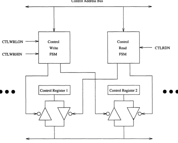
A block diagram of the Control Module is shown in Figure 2-1. The Control Module consists of two Finite State Machines (FSMs) to control read and write op-erations. In addition to the Control Write FSM and Control Read FSM, two generic control registers are shown in Figure 2-1. The Control Read FSM decodes the address on the control address bus during a read operation, and drives data onto the control data bus by enabling the output buffer of the appropriate control register. During a control write, the Control Write FSM decodes the address on the control address bus, and writes the data from the control data bus to the appropriate register by enabling the input buffer from the data bus to the register. Figure 2-1 is intended as a guideline and as a point of reference, and does not reflect the actual physical arrangement of the Control Module.
Control Address Bus CTLWRLON CTLWRHIN
*0
CTLRDN*0
Control Data Bus
Figure 2-1: Block Diagram of the Control Module
2.1 Hardware Implementation
The logic for the Control Module is encapsulated in an Altera EPLD, manufacturer part number EPM7192GC160-12. The primary control EPLD is designated U6, and is shown in section B of Figure B-3. This control EPLD manages most of the major control functions. The logic for the device is shown in Appendix C.2. This file contains all of the control logic that was used to implement the Control Module. It contains finite state machines to control register reads and writes, all Control Module control registers, and the logic to control an external serial electrically erasable programmable
read-only memory (E2PROM).
The E2PROM was used to implement an identification device for the PCB. The
EPLD file names, etc. The E2PROM is shown in section C1 of Figure B-3, manu-facturer part number X25040P. The Control Module can read or write information
serially to this E2PROM upon request through control registers. A hardware write
protection scheme was implemented to protect the information in the serial E2PROM
once it has been programmed. The signal IDWPOUTN functions as a write
pro-tect input for the serial E2PROM. A jumper, JP1, was inserted between the control
EPLD output for IDWPOUTN and the E2PROM's input. The E2PROM side of the
jumper was then tied to ground through a 4.7 KOhm resistor. During programming
of the serial E2PROM, the jumper should be installed, and the Control Module can
control the IDWPOUTN signal, driving it high during a write and low during write protection. Once the identification device has been programmed with the proper in-formation, the jumper can be removed from the PCB, and the IDWPOUTN input
to the serial E2PROM will stay grounded, protecting the programmed information
for future writes, regardless of the Control Module output. The Control Module can then read the true state of the IDWPOUTN signal as defined by the jumper before
it attempts to write to the serial E2PROM, preventing any accidental or extraneous
writes.
A transparent latch, manufacturer part number IDT74FCT573TSO, was used to latch the address presented on the control address bus, CTLADDR[5..0], from the control interface. The transparent latch is shown in section B3 of Figure B-3. The Control Module controls the latch enable signal, CADDRLE, allowing it to know precisely when the address is valid and invalid.
2.2
Control Register Memory Map
Operation of the TAXI-ISM is achieved primarily through writing and reading 16-bit control registers. All registers are either read/write or read-only. No write-only registers were implemented.
The TAXI-ISM implements a sixty-four register address space. Each register has a unique 6-bit address defined by the control address bus, CTLADDR[5..0]. Table A.1
shows the control register address map. Some registers are designated "Reserved for future use," meaning that they are currently undefined. Write operations to these registers will have no effect, and read operations of these registers shall return all zeroes. In addition, some bits within each register are also reserved. Write operations to reserved bits will have no effect, and read operations to reserved bits shall return all zeroes. All bits in each register default to zero upon reset or power up, except where specified.
Control registers were implemented as banks of DQ flip flops with enables, making them suitable for storage inside an EPLD. Since there are several EPLDs on the TAXI-ISM, it was more efficient to store relevant control registers in separate EPLDs instead of in a single EPLD; however, the main control EPLD, 13021, still manages all the control read and write operations.
The Control Module registers are stored in EPLD 13021, reference designator U6. These are located in address OxO0 (hex) to 0x09 and OxOC to OxiF.
Each Channel has its own specific registers. A separate EPLD was implemented for each channel. The Channel 1 registers are located at addresses 0x20 to 0x27, and these are contained in EPLD 12847, reference designator U5. The Channel 2 registers are located at addresses 0x30 to 0x37, and these are contained in EPLD
12847, reference designator U13.
The remaining registers belong to the Data Module. The BIT functions of the Data Module are contained in a separate EPLD. These registers are located at ad-dresses OxOA and OxOB, and are stored in EPLD 13022, reference designator U20. An additional set of registers called Ending Address Registers also belong to the Data Module. Ending address registers store the last address written by the Data Module incremented by one for the previous CPI, and are used to perform length calculations. They are located in addresses 0x28 to 0x2D, and are stored in EPLD 13035, reference designator U21.
2.3 Control Register Descriptions
This section describes the bit definitions of each of the TAXI-ISM control registers.
2.3.1 PCB Identification Control/Status Register
This register controls the reading and writing of the X25040P serial E2PROM, and
implements part of the PCB Identification Device as described in Section 2.1. This register is a 16-bit read/write register located at address offset 0x01. Bits 15 to 2 are reserved for future use.
Bits 2 to 1 implement the hardware write protection function discussed in Sec-tion 2.1. Bit 1 is the Control Module output for the write-protect signal to the serial
E2PROM. The Control Module can write a logic low (0) on bit 1 to attempt to put
the PCB Identification Device in write protected mode, or it can write a logic high
(1) to attempt to enable writing to the X25040P. Bit 2 shows the true state of the
serial E2PROM write enable signal, which is derived from the physical pin on the
X25040P.
Bit 0 implements a chip select function, whereby the Control Module can manually control the chip select of the X25040P chip. A logic low (0) deselects the X25040P,
and a logic high (1) selects the E2PROM.
2.3.2 PCB Identification Data Register
This register is used to provide the data interface to the X25040P serial E2PROM,
and is a 16-bit read/write register located at address offset 0x03. Bits 15 to 8 are reserved.
Bits 7 to 0 contain the data to interface with the X25040P. During a write to
the E2PROM, the data that will be written to the serial E2PROM is placed in this
register by the Control Module. During a read operation, the data that will be read
from the serial E2PROM will be placed in this register by the X25040P after a read
2.3.3 Control Register
This register is the primary control register for the TAXI-ISM. It is a 16-bit read/write register located at address offset 0x08. Bits 15 to 1 are reserved for future use.
Bit 0 controls the operation of the Receiver and Data Modules. When this bit is a logic low (0), operation of the Receiver and Data Module is suspended and the TAXI-ISM is put into an idle mode. No data is received by the Receiver Module
through the Receiver Interface, no data is written by the Data Module through the
Data Interface, and no error or status conditions are logged. When this bit is a logic high (1), the TAXI-ISM operates in a normal state.
The Control Module is not affected by the operation of this bit, and never enters an idle mode. All control registers will still function in idle mode. The purpose of this bit is to allow proper initialization of the TAXI-ISM without any interference from incoming data.
2.3.4 Error Register
This register is the primary error register for the TAXI-ISM, and logs all major card errors. It is a 16-bit register located at address offset 0x09. Bits 15 to 4 and 1 to 0 are reserved for future use.
Bit 3 represents a GBC Data Interface overflow. Data is written by the Data Module to the GBC card through the Data Interface, and eventually stored in GBC buffer memory. If an overflow of the GBC buffer memory is detected by the Data Module, this bit shall be written with a one, otherwise it shall be a zero.
Bit 2 represents a data loss error. If the TAXI-ISM detects that data has been lost, it shall set this bit. Data loss can occur as a result of a GBC Data Interface overflow (signified by bit 3), or if any of the Data Module address generators overflow (which will overwrite previous data causing the data loss).
2.3.5 Built-in Test Control Register
This register controls the operation of the Built-in Test function of the Data Module, and is a 16-bit read/write register located at address OxOA. Bits 15 to 12 are reserved
for future use.
Bits 11 to 7 determine the test pattern to be generated by the BIT function.
A value of ObOO00000 (binary) selects alternating data, where the bits of the pattern
alternate between 1 and 0. A value of Ob00001 selects pseudo-random noise patterns. All other values of bits 11 to 7 are reserved for future use.
Bits 6 to 1 determine the BIT duty-cycle. The BIT function simulates an ac-tive/inactive duty cycle of 1,024 writes to the GBC card. Table A.2 shows the defi-nitions for the duty-cycle selectors. For example, a selection of Ob000011 will select a duty-cycle of 512 active cycles and 512 inactive cycles. During the active portion
of the duty-cycle, the Data Module is free to send data to the GBC card through the
Data Interface. During the inactive portion of the duty-cycle, the Data Module will not send any data to the GBC card. This feature allows the TAXI-ISM to simulate bursty data streams, and test the variation of the Data Module to changes in data
rates.
Bit 0 enables or disables the BIT functions. A logic low (0) disables BIT functions; a logic high (1) enables BIT functions.
2.3.6 Built-in Test Base Pattern Register
This register specifies the base pattern used by the BIT function, and is a 16-bit read/write register located at address OxOB.
For the alternating data pattern, this register selects the initial value. For
ex-ample, if the base pattern register contains OxAAAA (hex), then the BIT function will generate the pattern OxAAAA, 0x5555, OxAAAA, etc. For pseudo-random noise patterns, this selects the initial seed a random number generator will use to generate
2.3.7 EPLD Identification Registers
This register is an EPLD identification register that contains the current revision level of the logic programs that were used to program each EPLD. Every EPLD on the TAXI-ISM is required to have an identification register. This register is a 16-bit read-only register. Bits 15 to 8 are reserved, and bits 7 to 0 contain the revision level. The initial revision shall have a value of zero. Subsequent revision levels shall have sequentially increasing values.
There are a total of six EPLDs on the TAXI-ISM printed circuit board: the Chan-nel 1 Receiver Module EPLD (12847), ChanChan-nel 1 Receiver Module EPLD (12847), Ending Address Register Controller EPLD (13035), Built-in Test Controller EPLD (13022), and Control Module EPLD (13021). The functionality of each of these EPLDs will be deferred to their relevant sections. The location of the respective identification registers is shown in Table A.1.
2.3.8
Channel Control Register
This register implements the control for the Receiver Module. Each channel has a Channel Control Register. The Channel 1 Control Register is located at address 0x21, and the Channel 2 Control Register is located at address 0x31. This is a 16-bit read/write register. Bits 15 to 8 are reserved.
Bit 7 serves as a reset bit to the memory buffers. This bit defaults to 1 after a card reset. A logic high (1) clears the memory buffer; a logic low (0) does not affect the memory buffer.
Bit 6 serves as a TAXIchip receiver reset. A logic high (1) causes the TAXIchip to reset its clock circuits and start receiving new data. A logic low (0) does not affect the TAXIchip. If asserted, this signal should be asserted for a minimum of 1 millisecond to ensure proper reset [1].
Bit 5 serves as a signal detect enable. The Receiver Module contains a signal detect that monitors whether or not an active fiber optic cable is connected to the input of the TAXI-ISM. If this bit is a logic high (1), then the Receiver Module will
ignore incoming data unless the signal detect signal verifies that an active fiber optic cable is connected to the input. If this bit is a logic low (0), then the Receiver Module will record all data regardless of the state of the signal detect.
Bits 4 to 3 define the number of bytes to use for frame synchronization. The Receiver Module scans the input stream for the frame synchronization bytes and sets
an appropriate status signal if it has found those bytes. A value of ObOO selects the
use of only one frame synchronization byte; Ob01 selects two bytes; OblO selects three bytes; Obll selects four bytes.
Bit 2 defines the byte-to-word sequencing mode of the Receiver Module. If this bit is a logic high (1), then the byte-to-word sequencing is reset when the TAXIchip receives a valid synchronization signal. A logic low (0) will not affect the byte-to-word sequencing.
Bits 1 to 0 define the method of byte-to-word sequencing. The Receiver Module takes two sequential input bytes and sequences them into a single 16-bit word. A value of Ob0 disables the byte-to-word sequencing; Ob01 selects the first byte received as the most significant byte, and the second byte as the least significant byte; OblO selects least significant byte first, most significant byte second; Obll is reserved for future use.
2.3.9 Channel Status Register
This register contains the status flags for the Receiver Module. Each channel has a Channel Status Register. The Channel 1 Status Register is located at address 0x22, and the Channel 2 Status Register is located at address 0x32. This register is a 16-bit read-only register. Bits 15 to 2 are reserved for future use.
Bit 1 records the status of the Receiver Module frame synchronizer. This bit is set if the Receiver Module has detected the number of frame synchronization bytes specified by bits 4 to 3 of the Channel Control Register.
Bit 0 records the status of the TAXIchip. This bit is set if the TAXIchip receives valid synchronization.
2.3.10
Channel Frame Synchronization Byte Registers
These registers provide the synchronization bytes that the Receiver Module can use for frame synchronization. There are four possible bytes that the Receiver Module can use for Frame Synchronization. Each byte can be selected by selecting the appropriate
mode using bits 4 to 3 of the Channel Control Register.
Each channel has four Channel Frame Synchronization Byte Registers. Channel 1's Frame Synchronization Byte Registers are located at addresses 0x23, 0x24, 0x25, and 0x26. Channel 2's Frame Synchronization Byte Registers are located at addresses
0x33, 0x34, 0x35, and 0x36.
These registers are 16-bit read/write registers. Bits 15 to 8 of each register are reserved for future use. Bits 7 to 0 contain the actual frame synchronization byte.
2.3.11
Channel Receiver Error Register
This register contains the Receiver Module receiver errors. Each channel has a Chan-nel Receiver Error Register. The ChanChan-nel 1 Receiver Error Register is located at address 0x27, and the Channel 2 Receiver Error Register is located at address 0x37. This is a 16-bit read/write register. Bits 15 to 4 are reserved for future use.
Bit 3 records if an overflow has occurred in the channel address generators, i.e. if the address counters have passed their maximum address limit. Bit 2 records if the channel buffer memory overflows due to a buffer full condition. Bit 1 records if an error occurs during the fiber optic relaying of an input byte. Bit 0 records if a signal
loss has occurred.
2.3.12
Channel Ending Address Low Register
This register serves to record the low sixteen bits of the ending address for each channel. The ending address is the last address written to the GBC card by the Data Module before a new CPI is initiated, incremented by one. The ending addresses can then be used in length calculations, recording the number of bytes written by each channel during the previous CPI.
The addresses written to the GBC card are twenty-two bits wide, so the ending address was divided across two registers, a low and a high, since registers are only sixteen bits wide. Each channel has a Channel Ending Address Low Register. The Channel 1 Ending Address Low Register is located at address 0x28, and the Channel 2 Ending Address Low Register is located at address 0x2A. This is a 16-bit read-only register. Bits 15 to 0 contain the low sixteen bits of the ending address.
2.3.13
Channel Ending Address High Register
This register serves to record the high six bits of the ending address for each Channel. Each channel has a Channel Ending Address High Register. The Channel 1 Ending Address High Register is located at address 0x29, and the Channel 2 Ending Address High Register is located at address 0x2B.
This is a 16-bit read-only register. The Ending Address Register defaults to the base address of each channel's address space after a card reset; 0x000000 for Channel 1 and 0x200000 for Channel 2. As a result, the Channel 2 Ending Address Register High Register defaults to 0x0020 after a card reset. In addition, the Channel 2 Ending Address High Register has one more bit than Channel 1 because the ending address for Channel 2 can be as high as 0x400000 (Ox3FFFFF plus 1). Therefore, bits 15 to 6 of the Channel 1 Ending Address High Register are reserved for future use, and bits 5 to 0 contain the high six bits of the ending address for Channel 1. Bits 15 to 7 of the Channel 2 Ending Address High Register are reserved for future use, and bits 6 to 0 contain the high seven bits of the ending address for Channel 2.
2.4 Control Register Write Operations
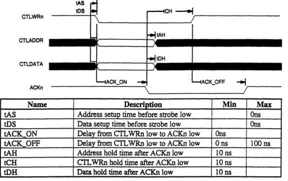
Control register writes are accomplished when the GBC card drives the control ad-dress and data buses, CTLADDR[5..0] and CTLDATA[15..0], to valid signal levels and asserts either of the control write lines, CTLWRHIN or CTLWRLON. All control registers are sixteen bits wide. Asserting either control write line independently will perform an eight bit write to the corresponding byte of the register, while leaving
tos tDS I CTLWRn CTLADDR CTLDATA ACKn . L-I Er1C tA ~tAH --ACKOFF -_i
Name Description Min Max
tAS Address setup time before strobe low Ons tDS Data setup time before strobe low Ons tACK ON Delay from CTLWRn low to ACKn low Ons
tACK OFF Delay from CTLWRn low to ACKn low 0 ns 100 ns tAH Address hold time after ACKn low 10 ns
tCH CTLWRn hold time after ACKn low 10 ns tDH Data hold time after ACKn low 10 ns
Figure 2-2: Control Register Write Interface Timing Specifications
the other byte unaffected. For example, asserting CTLWRHIN will write the data on the top byte of the control data bus to only the top eight bits (15 to 8) of a control register. Asserting both control write lines simultaneously will write all sixteen bits of the control data bus to the control register chosen by the CTLADDR[5..0] bus.
Once the Control Module completes writing to a control register, it asserts an acknowledge signal, ACKN, to signify to the GBC card that the write operation has completed. The Control Module will continue to assert the ACKN signal until both of the control write lines have been deasserted. A diagram specifying the timing constraints of a write operation is shown in Figure 2-2. Figure 2-2 details all of the timing guarantees for inputs to the Control Module involved in a control write operation, as well as all the timing constraints on the outputs of the Control Module.
I
II tDH eDMMI
f I -- ACK_ONA
|
2.4.1
Selecting Control Registers
Each group of control registers is selected by a combinational logic variable. The variable SELID is asserted (logic high) if the address on the control address bus designates the Control Module EPLD (13021) Identification Register, address 0x2F. The variable SELCTL is asserted if the control address bus is selecting a Control Module register, all of which are located in addresses 0x00 to OxOF (see Table A.1). The variable SELCHN is asserted if the control address bus is selecting a channel register. All of the Channel 1 and 2 control registers are located in addresses 0x20 to 0x27 and 0x30 to 0x37, all of which are of the form Obl*0*** (where * denotes a don't care). Using this strategy, the variable SELCHN is asserted if bits 5 and 3 have the values of 1 and 0, respectively. The variable SELRES is asserted if any other control register is selected by the control address bus, i.e. those registers in addresses
0x28 to 0x2E.
The latch enable signal for the control address bus transparent latch was im-plemented by logically ANDing the control read signal CTLRDN, the control write signals CTLWRLON and CTLWRHIN, and the acknowledge signal ACKN. In this manner, the address will be held valid by the transparent latch throughout an en-tire control read or write operation, from the assertion of the control signal to the deassertion of the acknowledge signal.
2.4.2 Control Write Finite State Machine
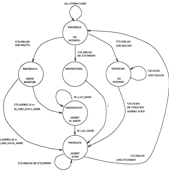
An independent finite state machine (FSM) was implemented in the Control Module EPLD (13021) to manage control writes. This FSM is designated WRITEFSM. The control write FSM consists of six states: WRITEIDLE, WRITEDATA, WRITEID-WAIT, WRITECHN, WRITENOTSEL, and WRITEACK. A state diagram of the control write FSM is shown in Figure 2-3.
The WRITEIDLE state waits for a control register write operation to begin. If both control write lines are inactive, then the FSM stays in the WRITEIDLE state. If the variable SELCTL and the control write line CTLWRLON are asserted, then
Figure 2-3: State Diagram of the Control Write FSM
a Control Module register is selected and the write FSM will transition to the state WRITEDATA. If SELCHN and CTLWRLON are asserted, then a channel control register is selected and the write FSM will transition to the state WRITECHN. If either CTLWRHIN or CTLWRLON is asserted and none of the selector variables are asserted, then the selected register is not in the Control Module EPLD or the Channel 1 and 2 Receiver Module EPLDs, and the write FSM transitions to the state
WRITENOTSEL.
The WRITEDATA state writes data to Control Module control registers. A case statement in the WRITEDATA state writes the data on the low byte of the control
data bus to the selected control register. An additional wait state is required if the selected register is the PCB Identification Data Register, since writing to this register
initiates a write cycle to the X25040P serial E2PROM. If this register is selected, the
write FSM will transition to the WRITEIDWAIT state, otherwise it will transition
to the WRITEACK state.
The WRITEIDWAIT state initiates and waits for the completion of a write
cy-cle to the serial identification E2PROM. A variable IDWRITE initiates the serial
write operation, and a variable IDLAGDONE signifies the end. The
WRITEID-WAIT state first asserts ID-WRITE, and then remains in this state until the variable
IDLAGDONE is a logic high. The write FSM then transitions to the WRITEACK
state.
The WRITECHN state manages writes to the Channel and 2 control registers.
The Receiver Module EPLDs perform the actual writing of the channel registers, and then assert a channel acknowledge signal at the end of the write cycle. The Chan-nel 1 and 2 control write acknowledges are provided by the variables CHiACK and CH2ACK, respectively. The WRITECHN state waits for both of these acknowledges to become asserted before proceeding to the state WRITEACK.
The WRITENOTSEL state is a wait state to allow for all control register writes besides Control Module and channel registers to complete. Since all other modules operate on the same system clock as the Control Module, only a single FSM state is required to allow the completion of a control register write.
The final state in the write FSM is the state WRITEACK. The WRITEACK state acknowledges the completion of a control write to the GBC card. This is done by asserting the signal ACKN. This acknowledge is asserted until both control write lines have been deasserted. Once this has occurred, the write FSM transitions back to the state WRITEIDLE, where it waits for another control write to occur.
2.4.3 Other EPLD Control Write Finite State Machines
Since the control registers are spread across several EPLDs on the TAXI-ISM, each EPLD that contains a control register has its own simplified version of the Control Module WRITEFSM to manage writing of the data to its own registers. All the indi-vidual finite state machines collectively perform a control write operation and make up the Control Write FSM shown in Figure 2-1. The main Control Module WRITEFSM still manages the overall control write operation, but these EPLDs "snoop" the ad-dress bus to see if the register selected is their own register and perform the actual register writes.The Channel 1 and 2 Receiver Module EPLDs (12847) and Built-in Test Function EPLD (13022) both have their own simplified write FSMs to perform the writing of their respective registers.
Channel 1 and 2 Receiver Module EPLDs (12847)
The Channel 1 and 2 Receiver Module write FSM is also designated WRITEFSM, and is shown in the EPLD file contained in Appendix C.1. The state diagram is similar to that of the main control write FSM shown in Figure 2-3, and is omitted. A main difference is that this FSM contains only three states: WRITEIDLE, WRITEACK, and WRITEWAIT. A similar selector variable, FNSEL, is asserted if a Channel 1 or
2 register is selected.
The WRITEIDLE state waits for a control write operation to occur. If the variable FNSEL is asserted, then the channel EPLD knows that a write to one of the channel registers is occurring. The write FSM writes the data to the appropriate register, and transitions to the WRITEACK state. If a control register write is occurring but FNSEL is not asserted, the write FSM will transition to the WRITEWAIT state.
The WRITEACK state acknowledges the completion of a channel register write to the Control Module WRITEFSM by driving the channel acknowledge signal, CH1ACKN or CH2ACKN. It waits for the control write line to become deasserted, and then transitions to the WRITEIDLE state to wait for another control register
write operation.
The WRITEWAIT state serves as a wait state for those writes to registers that are not channel registers. It waits for the control write line to become deasserted, and then transitions to the WRITEIDLE state to wait for another control register write operation.
Built-in Test Controller EPLD (13022)
The Built-in Test Controller EPLD write FSM is also designated WRITEFSM, and is shown in the EPLD file contained in Appendix C.3.3. The state diagram is similar to that of the main control write FSM shown in Figure 2-3, and is omitted. A main difference is that this FSM contains only five states: WRITEIDLE, WRITEHILO, WRITELOW, WRITEHIGH, and WRITEWAIT. Another difference is that the BIT write FSM is responsible for writing the high byte of control registers, since the Built-in Test Base Pattern Register is one of the few registers that utilizes the top byte (see Section 2.3.6). A similar selector variable, SELBIT, is asserted if a BIT register is selected.
The WRITEIDLE state waits for a control write operation to occur. If the variable SELBIT is asserted, then the BIT EPLD knows that a write to one of the BIT registers is occurring. The write FSM transitions to the state WRITEHILO if both control write lines are asserted, WRITELOW if only CTLWRLON is asserted, and WRITEHIGH if only CTLWRHIN is asserted. If a control register write is occurring but SELBIT is not asserted, the write FSM will transition to the WRITEWAIT state.
The WRITEHILO state performs a 16-bit write operation to the selected BIT register. Once the write is complete, the FSM transitions to the state WRITEWAIT.
The WRITELOW state performs a 8-bit write operation to the low byte of the selected BIT register. Once the write is complete, the FSM transitions to the state WRITEWAIT.
The WRITEHIGH state performs a 8-bit write operation to high byte of the selected BIT register. Once the write is complete, the FSM transitions to the state WRITEWAIT.
The WRITEWAIT state serves as a wait state for those writes to registers that are not BIT registers. It waits for the control write lines to become deasserted, and
then transitions to the WRITEIDLE state to wait for another control register write
operation.
2.5 Control Register Read Operations
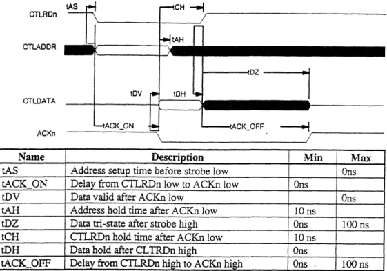
Control register reads are accomplished when the GBC card drives the control ad-dress bus, CTLADDR[5..0], to a valid signal level and asserts the control read line, CTLRDN. All control registers reads are sixteen bits wide. When the appropriate register has been located, the Control Module will drive the data inside the register onto the control data bus.
Once the Control Module drives the contents of the selected control register onto the control data bus, it asserts an acknowledge signal, ACKN, to signify to the GBC card that the read operation has completed and valid data is on the control data bus. The Control Module will continue to assert the ACKN signal until the control read line has been deasserted. A diagram detailing the timing specifications of a read operation is shown in Figure 2-4. Figure 2-4 details all of the timing guarantees for inputs to the Control Module involved in a control read operation, as well as all the timing constraints on the outputs of the Control Module.
2.5.1
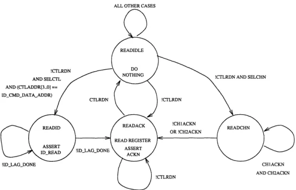
Control Read Finite State Machine
An independent finite state machine (FSM) was implemented in the Control Module EPLD to manage control reads. This FSM is designated READFSM, and consists of four states: READIDLE, READID, READCHN, and READACK. Selection of the control registers to be read is performed in the same manner as described in Section 2.4.1. A state diagram of the control read FSM is shown in Figure 2-5.
The READIDLE state waits for a control register read operation to begin. If the control read line is inactive, then the FSM stays in the READIDLE state. During a control read operation, a case is performed on the selection variables to determine
CTLRDn
CTLADDR
CTLDATA
ACKn
Name Description Min Max
tAS Address setup time before strobe low Ons tACK ON Delay from CTLRDn low to ACKn low Ons
tDV Data valid after ACKn low Ons
tAH Address hold time after ACKn low 10 ns
tDZ Data tri-state after strobe high Ons 100 ns tCH CTLRDn hold time after ACKn low 10 ns
tDH Data hold after CLTRDn high Ons
tACK_ OFF Delay from CTLRDn high to ACKnhih ... ns .. 100 ns
Figure 2-4: Control Register Read Interface Timing Specifications
which type of control register is being requested. If the PCB Identification Data Register is selected, then the read FSM will transition to the READID state. If a channel register is selected, then the read FSM will transition to the state READCHN. If any other register is selected, then the read FSM will transition immediately to the state READACK, where it will assert the acknowledge signal once the selected register's contents have been driven onto the control data bus.
The READID state initiates and waits for a read cycle to the serial identification
E2PROM to complete. A variable IDREAD initiates the serial identification read
cycle, and a variable IDLAGDONE signifies the end. The READID state first
initiates the read cycle by asserting IDREAD, and then remains in this state until
the variable IDLAGDONE is a logic high. The read FSM then transitions to the
READACK state.
The READCHN state waits for reads from the Channel 1 and 2 control registers to complete. The Receiver Module EPLDs perform the actual reading of channel regis-ters, and assert a channel acknowledge signal once this operation has completed. The
ALL OTHER CASES !CTLRDN AND SELCTL AND (CTLADDR[3..0] == ID_CMDDATAADDR) !CTLRDN AND SELCHN !CTLRDN !CHIACKN OR!CH2ACKN !ID_LAGDONE !CTLRDN
Figure 2-5: Control Read FSM State Diagram
Channel 1 and 2 control read acknowledges are provided by the signals CH1ACK and CH2ACK, respectively. The READCHN state waits for both of these acknowledges to become asserted before proceeding to the state READACK.
The READACK state drives the contents of the appropriate control register onto the low byte of the control data bus and asserts the control acknowledge signal. This state performs a case on the control address bus to select the correct register. If any of the channel registers or those registers that do not belong to the Control Module are selected, the READACK state does not drive the control data bus, and instead lets the appropriate EPLD drive the bus. It still asserts the acknowledge signal to signify valid data is on the bus. Once the control read line has been deasserted, the read FSM will transition back to the initial READIDLE state and wait for another control register read operation to begin.
The logic implementing the control readFSM is shown in Appendix C.2.
CHIACKN AND CH2ACKN