HAL Id: tel-03125275
https://tel.archives-ouvertes.fr/tel-03125275
Submitted on 29 Jan 2021HAL is a multi-disciplinary open access
archive for the deposit and dissemination of sci-entific research documents, whether they are pub-lished or not. The documents may come from teaching and research institutions in France or abroad, or from public or private research centers.
L’archive ouverte pluridisciplinaire HAL, est destinée au dépôt et à la diffusion de documents scientifiques de niveau recherche, publiés ou non, émanant des établissements d’enseignement et de recherche français ou étrangers, des laboratoires publics ou privés.
Compact multiscale modeling of carbon-based
nano-transistors
Yi Zheng
To cite this version:
Yi Zheng. Compact multiscale modeling of carbon-based nano-transistors. Electromagnetism. Sor-bonne Université, 2018. English. �NNT : 2018SORUS518�. �tel-03125275�
Sorbonne Université
Ecole doctorale : Science Mécanique Acoustique Electronique et Robotique
(SMAER)
Laboratoire d’Electronique et Electromagnétisme
Compact Multiscale Modeling
of Carbon-Based Nano-transistors
Par Yi ZHENG
Thèse de doctorat d’Électronique
Présentée et soutenue publiquement le 19/12/2018
Devant un jury composé de :
M. Philippe Dollfus, Directeur de recherche CNRS Rapporteur M. Thomas Zimmer, Professeur des Universités Rapporteur M. Stéphane Clenet, Professeur des Universités Examinateur M. Marco Saitta, Professeur des Universités Examinateur M. Zhuoxiang Ren, Professeur des Universités Directeur de thèse M. Guido Valerio, Maitre de Conférences HDR Co-encadrant de thèse M. David Brunel, Maitre de Conférences Co-encadrant de thèse
1
Dédicace
This research is dedicated:
To my supervisors: Associate Prof. Guido VALERIO, David BRUNEL, and Prof. Zhuoxiang REN, for their valuable instructions and suggestions.
To my parents: my father “ZHENG Bo” and mother “LI Jingzhong”, for their understanding, respecting my choice and caring for me.
To my husband: HungChyun CHOU, thank you for sharing your experience, giving me support without any complaint.
2
Acknowledgements
First and foremost, I would like to express my deep appreciation to my supervisors: Associate Prof. Guido VALERIO and Prof. Zhuoxiang REN for their patient guidance and suggestions. Without their invaluable help and generous encouragement, this thesis would not have been accomplished. I am grateful to Associate Prof. David BRUNEL for supervising me with advice and experimental resources on my thesis.
I am also thankful to the members of jury; particularly the reviewers M. Philippe Dollfus and M. Thomas Zimmer who gave me very useful recommendations, and M. Stéphane Clenet and M. Marco Saitta.
Besides, I wish to thank my colleague Fernando ZANELLA, I often have warm discussion with him about graphene modeling, who also built the model by different method.
Also, I would like to express my sincere gratitude to China Scholarship Council (CSC) for providing me opportunity to complete this work.
Last but not least, I would like to express my special thanks to my beloved parents and husband, whose care, endless love and support motivate me progress and make me want to be a better person.
3
Contents
Acknowledgements ... 2 Contents ... 3 Abstract ... 5 Chapter 1. Introduction ... 7 1.1 Research background ... 71.2 Electronic properties of a graphene sheet ... 11
1.3 Energy bands of graphene nanoribbons ... 16
1.4 Review of modeling methods for nano-transistors ... 18
1.4.1 Carrier transport model in GFET ... 19
1.4.2 Analytical models for GFET ... 20
1.5 Modelling methods used in this thesis ... 22
1.5.1 Micromodel: the Non-equilibrium Green’s function ... 24
1.5.2 Micromodel: the Semi-analytic multiscale approach ... 27
1.6 Approximated quantities describing nanoribbon energy-bands ... 28
1.7 Research Objectives ... 31
1.7.1 Graphene nanoribbon based transistors ... 31
1.7.2 Graphene nanomesh based transistors ... 33
Chapter 2. Dispersion Relations under Deformation and Schottky Field-Effect Transistor .... 36
2.1 Energy bands of a deformed graphene nanoribbon ... 36
4
2.3. Deformations in Schottky Field-Effect Transistor ... 48
2.4 Study of deformation effects on carbon-based transistors with Semi-Analytic and Ab-Initio Models ... 49
2.5. Semi-analytical multiscale coupled modeling ... 53
2.5.1 A short discussion on the tight binding model without variation of hopping parameters ... 54
2.5.2 The full model of deformation: the Ballistic regime ... 59
2.5.3 Partially Ballistic regime ... 68
2.5.4 On/Off current ratio and differential conductance with different deformations ... 73
2.5.5 Shift of transfer characteristics with different SB height ... 76
Chapter 3. Application of Nanomesh in Field-Effect Transistor ... 78
3.1 Graphene nanomesh and its electronic properties ... 78
3.2 Compact model validation with ab-initio method ... 83
3.3 Graphene nanomesh transistor and its I-V characteristics ... 88
3.4 Numerical and experimental study of graphene nanomesh transistor ... 93
Conclusions and Perspectives ... 99
Annex: Experiments on graphene transistors at Chang Gung University ... 101
A.1 Chemical Vapor Deposition (CVD) method to produce graphene and graphene transfer technology ... 101
A.2 Deformation of pristine graphene based transistor in CGU ... 102
List of Publications ... 106
5
Abstract
Among emerging carbon materials, graphene has rapidly become an ideal candidate for nano-electronics. In this context, different methods have been proposed to transform its electric properties and remove the Dirac degeneracy point, leading to application to nano-transistors. In this thesis we apply a semi-analytical compact model to study two kinds of graphene-based nanotransistors: nanoribbon graphene transistor and nanomesh transistor. A tight-binding model is used to determine analytical expressions for the energy bands of a graphene nanoribbon. Comparisons are shown with ab-initio approaches and with measurements done on larger-scale transistors of the same kind.
In the context of flexible electronics, mechanical stresses on circuits and subsequent geometric deformations of graphene-based components is an important issue. We investigate these effects on the conduction properties of nanoribbon transistors (both in ballistic and partially ballistic regimes). By assuming the presence of small deformations, a spectral scaling and a spectral shift due to the presence of a deformation can be taken into account analytically. This model leads to define in closed form effective quantities (masses, densities of states) used to numerically calculate potentials and currents in the nano-device. Numerical results are shown both in a ballistic and partially-ballistic regime, with and without the presence of Schottky contacts. The proposed results in Chapter 2 illustrate in a very simple way how the deformation of graphene nanoribbon influences the I-V characteristics of transistor.
Another solution to realize graphene nanotransistor is the etching of nanoholes in a graphene sheet (thus realizing a nanomesh). If graphene nanomesh is properly shaped, the On/Off current ratio of transistor is expected to be enhanced. In Chapter 3, the semi-analytic method is used to evaluate the performance of nanomesh transistor with nanoribbon ones. The results are again compared with an ab-initio method. I-V characteristics of graphene nanomesh transistor are presented and compared with experimental results. The proposed results show how graphene nanomesh size influences the I-V characteristics of transistor.
6 Given the simplicity and the reduced computation time of the approach, these results can lead to perform parametric analyses, optimizations and characterization of graphene nano-transistor when applied in larger-scale circuits.
7
Chapter 1. Introduction
In this chapter, we give some introductory notions about the interests of graphene, its application in electronics, and the modelling tools to predict its electronic behaviour in nano-transistors. Namely, the tight binding model is introduced and discussed, leading to compute the conduction bands of graphene and its properties. A brief review of modelling methods for transistors is also given, together with their fields of application. A semi-analytic method for carbon-based nanotransistors is then described with some details, being the approach chosen for the study of the devices analysed in the following chapters.
1.1 Research background
Materials can be classified into three categories with respect to their electronic properties, according to the shape of energy band around the Fermi level (i.e., the approximate energy level of charged carriers). Conductive materials (such as copper, iron, etc.) enable the conduction of electric currents since an energy level is present around the Fermi level. This band offers the carriers free degrees of states to create a current flow. Insulator materials (such as ceramics, plastics, etc.) do not allow electric current to flow, since the Fermi level falls in an energy gap and no close available energy bands allows the conduction of current. Finally, semiconductor materials (such as Germanium, Silicium, etc.) can conduct current if some external energy is provided to carriers in order to overcome the small energy gap around the zero-Kelvin Fermi level. Figure 1.1 shows different band gaps in metals, isolators and semiconductors. Semiconductor materials were discovered in the 19th century; however it did not arouse researcher attention at that time. Due to the development of radar technology in World War II and electronics, semiconductor materials played a fundamental role in technology advancements and stimulated a considerable amount of research activities.
Semiconductor materials are in fact of crucial importance for today’s electronic technology as the development of integrated circuit is based on it. Figure 1.2 shows some important steps of the development of semiconductor devices going from the discovery of semiconductor properties to the invention of transistor and the development of modern electronic circuits. Vacuum tubes were once the basic components of electronic devices for
8 signal amplifications and mixing. However, their large volume and fragility would hinder the development of miniaturized and embedded circuits. In this context, the emergence of semiconductor transistors was the greatest breakthrough leading to electronic devices of smaller size, lower cost, reduced power-consumption and heat dissipation. The appearance of the first transistor in 1947 at Bell Labs marked the beginning of the electronic era [1]. In 1958, integrated circuits were invented by Jack Kilby, when it became possible to place many transistors on the same chip. In 1965 Gordon Moore, one of Intel’s founders, observed that that the number of components in an integrated circuit is doubled every 18-24 months while the overall price of the circuit being constant [2]. This was later acknowledged as the well-known Moore's Law, describing the evolution of the electronic technology of the rest of the century.
Figure 1.1: Bandgap of different kind materials.
Following Moore’s Law, the miniaturization of transistors proceeded at a steady pace in the last decades. Nowadays limitations of bulk MOSFET are arising to short-channel effects that slow down the miniaturization of devices. Effects such as the saturation velocity of charges and the lowering of threshold voltage limit the performance of devices at nano-scale. In this framework, carbon-based nano-transistors have recently attracted a lot of attentions due to their tiny sizes and remarkable electronic properties [3]-[5]. In [3], P. Avouris et al. studied the performance of carbon nanotubes (CNTs) transistors. The electronic characteristics of CNTs transistors (gate length 260 nm) are compared with two silicon devices, proving that CNTs transistors can have superior on-off current ratios and better transconductance than silicon transistors. In [4], R. Martel et al. also presented some experimental data of nanoscale carbon-based transistors. Different electronic characteristics of
9 carbon-based transistors are compared with 25 nm Si FETs and 100 nm Si FETs respectively, the improved performance of carbon-based transistors demonstrated that they may be competitive with Si FETs [4]. Moreover, even if great progresses have been achieved for the realization of Si-based devices, their gate length and gate insulator thickness cannot be continuously scaled. The unique electronic properties of carbon based material offer the possibility to overcome these limitation and achieve further device miniaturization.
Figure 1.2: Events during the development of semiconductor devices.
The design of novel electronic devices for diverse applications, such as biomedical, security or leisure, must face several challenges, notably in terms of flexibility, biocompatibility, and low power consumption. In this framework, thanks to the electric properties of graphene, graphene-based transistors are currently regarded as an attractive solution of these issues.
There are already several cases of graphene implementation in industry engineering (see Figure 1.3). Graphene can be used e.g. as the coating material of touch screens for telephones and computers [6]. If we apply graphene in our computers, the new material will make them much fast [7]. Graphene-based patch can also be used for monitoring possibly treats diabetes [8]. It can maintain healthy blood glucose levels in people through measuring the sugar in sweat and delivering necessary diabetes drugs through the skin.
10 Furthermore, electronic properties of graphene are not the only advantages of this material. Due to mechanical robustness and flexibility, carbon-based transistors are natural candidates for different electronics (see Figure 1.3 and Figure 1.4).
Figure 1.3: Properties of graphene and its potential applications.
Figure 1.4: (a) Graphene-treated nanowires could replace current touchscreen technology
(b) A graphene patch that monitors and possibly treats diabetes [9][10].
11
1.2 Electronic properties of a graphene sheet
Graphene is a two-dimensional material consisting of hexagonal carbon atoms arranged in honeycomb lattice (see Figure 1.5) [11]-[12]. More specifically, it is an allotrope of carbon in the structure with a molecule bond length of 0.142 nm. Since mechanical exfoliation of monolayer graphene was first reported in 2004 by Andre Geim and Konstantin Novoselov [13], interest in this material has increased dramatically. Compared with other materials, graphene has many excellent properties, which are shown in Table 1.1.
Figure 1.5: Shape and characteristics of graphene [14].
Table 1.1: List of typical graphene properties.
Graphene Property Numerical Value Comparison with other material
Tensile Strength ~130 GPa [15] steel ~550 MPa [17]
Young’s Modulus ~1 TPa [15] Bronze ~ 96–120 GPa [18]
Thermal Conductivity ~5000 Wm-1K-1 [16]
Diamond: ~ 1000 Wm-1K-1 [19]
Copper: ~ 401 Wm-1K-1 [19]
Electron mobility excess of cm2/(V·s) [11]
Si ~ 1400 cm2/ (V·s) [20]
The graphene primitive cell is shown in Figure 1.6, where each blue point is a carbon atom, and green lines join adjacent atoms. In order to develop an analytical expression for the
12 energy band structure of graphene the time-independent Schrödinger’s equation should be solved,
H
k,r E
k
k,r (1.1) where 𝜓 is the electron wavefunction, H is the Hamiltonian operator which operates on the wavefunction and the energy E is its eigenvalue. k=kx x+ky y is the wavefunction momentum,also called reciprocal vector. Models for the computation of energy bands of graphene structures can be based on first-principle or on tight binding approaches. In both cases we aim at solving the Schrödinger equation.
Figure 1.6: Schematic illustration of a graphene cell.
First principle models aim at solving the Schrödinger equation by using only physical fundamental constants and the atomic composition of the material as input. They allow the computation of several quantities of interest in solid-state physics and chemistry, namely the electron density, energy levels, and nuclei positions, leading in our case to a precise characterization of electric features of nano-devices. Due to the extreme complexity of the calculation (large number of unknowns, of variables of wave functions, non-linear nature of the problem and iterative solutions required, etc.) many ab-initio approaches exists, depending on the specific assumptions used to simplify the problem under study. Among the best known is the Hartree–Fock (HF) method and its variations. It uses the so-called Born-Oppenheimer approximation, consisting in a two-step solution of the time-independent Schrödinger
13 equation separately for the electronic coordinates (with an “electronic” Hamiltonian) and for the nuclei coordinates (by including the nuclear kinetic energy). The unknown wave function is expressed as a sum of basis functions (“atomic orbitals”), chosen to approximate a complete basis in order to represent at the best the wave function. The Hartree-Fock ab-initio method is certainly among the most accurate and flexible modeling for a vast class of atomic structures. It allows getting accurate results at high energies, in the presence of irregular shapes, defects, loss of symmetry. However, due to the complexity of the problem and the number of different particle interactions, ab-initio calculation time becomes long as the size of the domain increases and prevents the simulation and the optimization of large devices. Thanks to the symmetry of the graphene lattice, nano-electronic applications presented in this thesis can be often modeled, at least partially, with simplified methods leading to fairly accurate results.
- Tight binding model
Tight binding theory can overcome limitations of ab-initio simulations and even give analytic closed-form results, which can help us gain a physical insight about the device operation. It leads to the electronic structure of the material under study, by solving also in this case the time-independent Schrödinger’s equation for the energy dispersion band structure.
The tight binding model is a method of calculating the electronic band structure by using a set of approximate wave functions which are based on superposition of isolated atomic wave functions. This model is different from free electron model. For nearly-free electron model, interactions between electrons are ignored and assume the electrons in the crystal only have weak Coulomb attraction from respective nucleus [12]. On the contrary, in tight binding model we assume that the atom has a strong binding effect on electrons. Electrons near the atom are mainly affected by the potential field due to the atom, while the effect of other atoms is regarded as a small perturbation.
In order to obtain simple closed-form results, leading to a fast analysis tool, in this thesis we choose to use a tight binding model for solving the electronic structure of deformed graphene. Furthermore, the method can be used also to calculate the modification of energy bands due to small deformations of the graphene lattice. In the following the main results
14 obtained with the tight binding approach are summarized. More details and calculations about the effect of deformations will be presented in Chapter 2.
A tight binding model can be considered to solve (1.1), consisting in retaining only a finite number of mutual interactions among atoms in the Hamiltonian H [12]. If only the closest atoms interact, a so-called nearest-neighbor approach is obtained. In this case, the spectral Hamiltonian becomes:
H
k V e
jk R1 e jk R2e jk R3
(1.2)with the tight-binding hopping parameter V=2.7 eV, experimentally determined, describes the energy related to an electron exchange between adjacent sites. V is also referred to as the nearest neighbor overlap energy, the hopping or transfer energy, or the carbon–carbon interaction energy [12]. Of course the symmetry of the lattice grants that the value of V is the same for all the possible exchanges with each of the three nearest neighbors.
In the nearest-neighbor approach, graphene energy bands can be computed from equation (1.2), [12].
E2
k V2
e jkR1e jkR2 e jkR3
ejkR1 ejkR2 ejkR3
(1.3)The hexagonal symmetry of the lattice makes it simple to express the vectors R1, R2,
and R3 as a function of the inter-atomic distance a = 2.46 Å (see Figure 1.6).
1 2 3 , 0 3 , 2 2 3 , 2 2 3 a a a a a R R R (1.4)
A simple replacement of (1.4) in (1.3) leads to the final expression:
3 2, 1 4 cos cos 4cos
2 2 2 x y x y y a a a E k k V k k k (1.5)
15 Figure 1.7 shows the bi-dimensional Brillouin diagram obtained with the nearest-neighbor tight-binding approach (1.5). The upper half dispersion is the conduction band and the lower half dispersion is the valence band. The K points, also called Dirac points, are the point in the kxky spectral plane where the conduction band and valence bands touch each
others exhibiting a locally linear behavior. Figure 1.8 shows the typical Dirac cone at the points K, where a locally linear dispersion is found. In Figure 1.8, the Dirac cone shows clearly that an infinite graphene sheet exhibits no band gap.
Figure 1.9 shows the comparison of an ab-initio and a nearest neighbor tight-binding (NNTB) model for graphene energy dispersion. The ab-initio model is of course more accurate than NNTB method. From Figure 1.9, we can observe subtle differences for higher energies. However, behavior of electrons around Dirac points is the most relevant to study transport properties in nano-transistors. Since ab-initio model and NNTB model show good agreement at low energies, tight binding method are currently used for these applications mainly due to the reduced computation time and ease of implementation, even if not being as accurate as ab-initio models.
16 Figure 1.8: The linear energy dispersion of graphene at the K-point.
Figure 1.9: Comparison of ab-initio and NNTB model for energy dispersions calculation [12].
1.3 Energy bands of graphene nanoribbons
Graphene nanoribbons are narrow rectangles made from graphene sheets. Two main types of graphene nanoribbons can be considered, the armchair GNRs (aGNRs) and zigzag GNRs (zGNRs). The difference among them is that aGNRs has an armchair cross-section at its edges, while zGNRs has a zigzag cross-section at its edges [12]. An aGNR can be obtained by cutting a graphene sheet along a given direction (see Figure 1.10). Since the resulting strip lacks the translational symmetry along one direction (its width), no simple closed forms can be obtained for its energy bands as in the infinite-graphene case. However, if an ideal Dirichlet condition is enforced on the wavefunction at the opposite boundaries along the
17 width w = (𝑁 − 1)𝑎/2 of aGNR, where N is the number of tightly bound atoms in the direction of the ribbon width (y in Figure 1.10),
Figure 1.10: Armchair graphene nanoribbon.
ψ y ψ y w 0 2 2 a a (1.6)
simple conditions can be derived on the ky wavenumber for aGNR:
wa
ky,
π (1.7)
y, απ απ 2απ 1 a a a 1 a 2 k N w N (1.8) where α = 1,…, N.Once the discretized values of ky,α are replaced in the energy (1.5), the sub-band
structure of the nanoribbon is obtained:
3 2 V 1 4 cos 4 2 x x ak E k A A (1.9) where π cos 1 1, , A N N 18
1.4 Review of modeling methods for nano-transistors
The electronic and mechanical properties of graphene are the reason of the interest in based devices. The behaviors are of course related to the energy bands graphene-base structures, but also to other factors like deformation features, temperature of the environment, geometric and physical parameters of the device. Unfortunately, accuracy issues of current models for transistors are already arising in connection to the progressive reduction of the scale of MOSFET devices. This complexity motivates the research of numerical models efficient and at the same time accurate. Different models are briefly reviewed here, and more details will be given about the model selected to study the transistors in the following chapters.
The drift-diffusion model is the most common semi-classical models of micron-scale semiconductor devices [21][22]. The current flowing through the device is the sum of a drift term and a diffusion term both for electrons and holes. The success of the drift diffusion model is due to its efficiency, simplicity, and flexibility on different kind of meshes for arbitrary geometries. However, this model does not take into account quantum effects arising in nano-scale devices, such as hot carriers and band discretization due to spatial-confinement effects [23]. Different modifications have been proposed in order to introduce suitable corrections to these limitations.
Monte Carlo algorithms are the most reliable and established approaches, extensively used to simulate devices under semi-classical regimes. They are based on the simulation of a large number of sample cases (particles motion through the device) whose trajectory is computed with semi-classic approximations. Scattering phenomena intervals of free-flight (time intervals between scattering events) are computed with suitable statistics [24]. The scattering effects and velocity spectra are also studied for nano-scaled MOSFET (which channel lengths are 15nm and 25nm) by using Monte Carlo simulation in [25]. Recent works have shown how to successfully include quantum effects due to thin films (by means of sub-band quantization corrections) and short-channels effects (by including quantum non-local effects in the charge density evolution) [26].
Hydrodynamic models are derived by applying the moment technique to the Boltzmann transport equation. The propagations of electrons and holes in a semiconductor
19 device is here simulated as the flow of a charged compressible fluid [27][28]. This allows for considering the effect of hot carriers, which is missing in the drift-diffusion model, and leads to accurate results for devices of size larger than 0.05 m. Also in this case, quantum corrections to the evolution of the charge distribution have been proposed to treat smaller devices [29]. This approach is much faster than Monte Carlo ones, but can fail at very small scale, where Monte Carlo is still reliable. Thoma [28] proposed a generalized hydrodynamic model, where formulas depending on temperature only are applied.
In order to reduce the computation time and obtain simplified models to be used in circuit design and optimization, the intensive research on graphene field-effect transistors (GFET) stimulated within the past decades several models for better understanding characteristics of these devices and to reduce the computation time of rigorous approaches.
1.4.1 Carrier transport model in GFET
In [30], an analytical model for GFET is presented (see Figure 1.11). In this structure, the substrate is highly conducting and serving as the back gate, while the top gate controls the current. Thermionic transport is described for this kind of GEFT. Potential distribution in the channel and thermionic current are calculated accordingly by using this analytical model.
Figure 1.11: Schematic view of GFET structure studied by V. Ryzhii, M. Ryzhii, and T. Otsuji [30].
In [31] first principle approach is used to study the behavior of GFET, thus obtaining thermal, electrostatics, and electrodynamic quantities, channel current and transfer characteristics. Based on the physical model in [31], a small-signal model was proposed in [32]. This small-signal model is also based on first principle and the carrier transport in the
20 channel is studied by drift-diffusion model. S. Thiele and F. Schwierz proposed a simple model for calculating DC behavior of GFET [33]. Modeling results like transfer characteristics and output characteristics are successfully compared with experimental data.
In [34] the carrier transport is studied with a drift-diffusion perspective, for both single-layer and multiple-layer graphene. In [35] the non-equilibrium Green’s function (NEGF) technique is used to solve the Dirac equation for GFET, and the carrier transport of double-gate GFET is investigated.
1.4.2 Analytical models for GFET
In the last decade, some analytical models for GFET have also been proposed. The authors of [36] describe the design of top gate GFET [36] (as Figure 1.12 shows). In their research, the channel material is bandgap graphene. Although the utilization of zero-bandgap graphene limits the on-off current ratio, the results showed the possibility of applying graphene for radio frequency circuit.
Figure 1.12: Top gate GFET structure studied by I. Meric [36].
The carrier concentration n is at first computed, and the quantum capacitance is calculated as:
21
2Cq n/ e /Fħ (1.10)
where𝜈𝐹 is the Fermi velocity. The current in the channel can then be derived as:
0 L d drift W I en x v x d x L
(1.11)where W is the channel width, L is the channel width, 𝑣drift(𝑥) is the carrier drift velocity. The carrier drift velocity can be calculated by using a velocity saturation model:
1 / drift sat µE v x µE v (1.12)where 𝑣𝑠𝑎𝑡is the saturation velocity of the carriers. A considerable amount of later research is based on [36]. In [37] the gapless graphene is also used as channel material. Compared with [36], stable saturation is obtained.
Quantum capacitance, channel charge, I-V characteristics, the small signal parameter and cut-off frequency are all calculated in this model. These results are also validated with experimental data from long-channel GFETs (channel length larger than 1 μm).
A new compact model [38] is proposed based on the quasi-analytical model in [37] and verified by using measurements from the literature. The authors of [39] proposed a compact model suitable for short-channel GFETs (the channel length is 240 nm) and based on the concept of “virtual source”. This GFET virtual source model allows to study the carrier transport in GFETs and is also described in H. Wang’s model [39]. The derived I–V characteristics are compared with experiment data showing a good agreement.
In [40] and [41], a GFET model is presented for radio frequency applications, based on drift-diffusion theory with saturation velocity effects. Drain current, charge, and capacitance of GFET are there discussed. In [42], a semi-empirical model is shown for single layer zero-bandgap graphene. The current can be calculated by using carrier density, the carrier velocity, the channel length and the channel width. The carrier density is modeled by semi-empirical charge-voltage relation and carrier drift velocity is obtained by a velocity
22 saturation model. Compared with physical models, this semi-empirical model gives accurate drain and source contact resistances and can provide acceptable accuracy with considerably reduced time.
In [43], models for both monolayer graphene and bilayer graphene based on the results in [36][37] are presented. In [44] a compact model for GFET in the quantum capacitance limit based on the drift-diffusion model [44]. The results of [36] were also used in [45] and [46] to achieve a scalable compact model based on quasi-analytical physics, where the charge distribution computation is improved by considering the specific graphene density of states. This approach has inspired a number of following papers such as [47]. In [48], a circuit-level model for GFET is proposed which channel being either a multilayer graphene involving an arbitrary number of layers. The multilayer geometry is described with the introduction of a novel interlayer capacitance leading to an accurate calculation of the channel surface potential and the channel resistance. In [49] an ambipolar-virtual-source model for nanoscale GFET is presented, including two separate virtual sources for electrons based on drift-diffusion equation.
These models are mainly focused on the use of graphene in FET and they are suitable for analogue and radio frequency circuit without considering band gap. However, the lack of bandgap limits the on-off current ratio. Different methods to tune the band gap of graphene for FET have been proposed for practical application. The most appealing approaches, compatible with the realization of fully planar nanotransistors, is the cutting of graphene sheets into thin nanoribbons and the fabrication of nanomeshes by removing atoms along a periodic pattern. Graphene nanoribbon exhibits a band gap directly related to their width, and equivalently to the number of atoms along their transverse (and shorter) dimension. The bandgap of nanomesh is also related with its geometric features, namely the shape and distributions of the holes.
1.5 Modelling methods used in this thesis
In this section, we will introduce the two methods used in this Thesis to model the nano-transistors described later. In relation to the size of the transistors chosen, we aim at
23 analyzing the electronic characteristics of both ballistic and quasi-ballistic GFET. This means that the length of the device is smaller than the mean free path of graphene, so that charges move through the channel without experiencing any scattering (ballistic regime) or encountering a limited amount of scattering (partially ballistic regime).
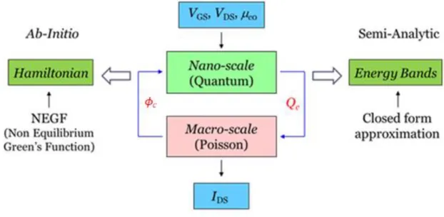
The objective of the model is the computation of the current under different voltage excitations. However, the current in can only be computed once the potential distribution along the channel (x) is known (x being a linear coordinate along the channel). This potential is a quantity varying along the channel in the case of quasi-ballistic transistor, or a constant along the channel in the case of ballistic transistor. In order to determine the potential, the charge distribution along the channel should be computed with two different approaches at different scales, and a multiscale coupling between them is performed. We have then a macro-model and a micro-macro-model. In order to obtain a coherent description of charge density, an equality is enforced between the charges computed with both models: this gives an equation leading to the numerical determination of the channel potential (x). This is described in Figure 1.13.
Figure 1.13: Diagram used in both models to compute source-drain current.
More specifically, the macro-model computes the charge distribution in the channel through an electrostatic analysis of the device. Its mathematical formulation is done through Poisson equation, but for canonical geometries as those studied here, analytic simplified
24 expressions for the capacitances between contacts can be used in order to avoid a full numerical solution of the Poisson equation.
In fact, a macroscopic expression for the charge, expressed through equivalent capacitances Cg, Cs and Cd can be written straighfowardly as:
FB,
, ,
macro c i i i c i g s d Q x C V V x (1.13)where Vg, Vs, Vd are the voltage of gate, source and drain, respectively, and VFB,i are the
relevant flatband voltages.
The g ate capacitance per unit area can be calculated as [50]:
ε ε0 π 1 ln 6 1 g r C t t w w (1.14)
where t is the thickness of the substrate (SiO2 in the following chapters) 𝜀𝑟 is its relative
permittivity, and 𝜀0 is the permittivity of vacuum. Note that this expression is quite different from the simple capacitance of a large parallel plate system, since fringing-field corrections are relevant at this length scale.
The micro-model computes the charge in the channel by means of a quantum approach, and its mathematical formulation is done by means of the Schrödinger equation. This micro-scale problem is formulated in two different ways. A rigorous but time-consuming ab-initio approach is chosen in order to obtain results to be used as a reference. However, in order to have a faster method useful for the parametric analysis and optimization of electronic devices, we use also a semi-analytic approach whose results will be compared with the ab-initio ones.
1.5.1 Micromodel: the Non-equilibrium Green’s function
A very accurate ab-initio method often used for the study of physical properties of materials and more specifically the behavior of nano-transistors is the Non-equilibrium Green’s function (NEFG). The NEGF approach is a dynamical formulation based on the solution of Schrödinger equation, solving for the energy bands of materials by describing the
25 interaction among atoms through proper atomic orbitals for the coupling between carbon atoms, and between the source/drain and the graphene [51]. Despite its accuracy and flexibility, this method is time consuming if compared with the analytic method described in the following paragraph 1.5.2. For this reason, the NEFG1 method will be used in this Thesis to obtain reference results with the aim of validating the analytic method proposed later.
The NEFG method performs the numerical solution of Schrödinger equation in the Laplace domain, thus keeping a full information on the dynamic properties of the device. An extensive treatment of NEGF can be found in [51][52]; here we give a few definitions necessary to formulate our problem.
The current of graphene nanoribbon-based FET can be calculated by the following equation [53]:
2 * * * S S c D D c S D q I trace G G f f dE
(1.15)where 𝚺𝑆 and 𝚺𝐷 are operators describing the interactions with S and D contacts, respectively,
fS and fD are Fermi distribution at the S and D contacts, respectively, G
c is the Green’s function, 𝜙𝑐 is the channel potential to be determined with the multiscale approach describedabove.
Every atom in the lattice can be indexed by a couple of integers, and the interaction between sites by the indices mn, ij. To apply (1.15) to a graphene channel, the equation of motion must be enforced for the Green’s function:
†
, , , , ,
r
t mn ij mn ij mn ij
i G t t tt i tt c H c (1.16)
and the operator H in (1.16) describing the electronic interactions is:
1 The method has been developed by Dr. Fernando ZANELLA, at the time PHD student at the Universidad
26 2 2 2 , 0 0 1 2 4 c i j c e i j q Z H m r R a (1.17)
where q is the electron charge and is the reduced Plank’s constant. The first term in (1.17) is the kinetic energy of each electron, whit me being the free electron mass. The second term
is the Coulomb potential between an electron and a carbon nucleus, with Zc the effective
atomic number and ε0 the vacuum permittivity; ri−Rj is the distance between an electron and a
nucleus, and a0 is the maximum radius of a carbon atom, significant when i = j. The last term
is the localized channel potential that must be found by coupling the quantum-mechanics equations with the electrostatic problem (Poisson equation). The Green’s function can be obtained by solving the Schrödinger equation in Laplace domain:
1 c S D G E j H (1.18) where E is the energy, and is an infinitesimal number necessary to guarantee convergence. To find the matrix form of 𝑯 we project (1.17) in a 𝜋 orbital basis for the channel given by
5
, cos r i j r e (1.19)where = 2.18 is a constant enforcing orthonormality. For the contacts, we consider a coupling between a carbon atom and gold atom.
We should notice this method is very accurate, but also time consuming and not suitable for fast analyses of circuits composed of several devices or optimization of devices with respect to several parameters. The method requires computational is related in the first place to the great number of interactions among orbitals considered.
27 1.5.2 Micromodel: the Semi-analytic multiscale approach
Therefore, in this thesis, we choose to apply ballistic transport model and partially ballistic transport model for analyzing the electronic characteristics of GFET. This means that the length of the device is smaller than the mean free path of graphene, so that charges move through the channel without experiencing any scattering (ballistic regime) or encountering a limited amount of scattering (partially ballistic regime).
An appealing model for nano-scale transistor in ballistic regimes (which can be easily extended to the semi-ballistic [54][55]) has been proposed in [51][56], based on the analytic calculation of energy bands and the density of states of nanoribbons. The current flowing in the transistor can be calculated by using a Landauer–Büttiker approach [51]:
max 0 , , * 0 d π E i i s d i c s E d T T q I f f E T
ħ (1.20)where Ts and Td are the transmission coefficient of charges through Schottky barrier at the
source and drain contacts, respectively, and become equal to one in the case of Ohmic contact. Their computation is detailed in next paragraph 1.6. The factor T* is given by
*
s d s d
T T T T T
In equation (1.20), i =e, h stays for electrons and holes, and the Fermi-Dirac distribution f is integrated:
1 1 f e
(1.21)
e α,s d b0
c s dE
q
x
E
k T
(1.22)
α,s dh
α,s de (1.23) 𝜇𝑠 and 𝜇𝑑 are the Fermi levels of source and drain respectively, E is the kinetic energy (to be integrated in (1.20)) and 𝜙𝑐(𝑥) is the surface potential, i.e., the potential along the channel.28 As said above, its dependency on x, a coordinate along the channel lengh, cannot be neglected in the case of partially ballistic conduction. 𝑘b is the Boltzmann’s constant and T is the temperature. The total current is given by:
𝐼 = 𝐼𝑒− 𝐼ℎ (1.24) However, before computing (1.20) and (1.24), the surface potential 𝜙𝑐 must be determined first. The surface potential 𝜙𝑐 can be determined by imposing a consistency relation between the mobile charges in the channel 𝑄𝑚𝑖𝑐𝑟𝑜(𝜙𝑐),computed with a
quantum-mechanical approach , and 𝑄𝑚𝑎𝑐𝑟𝑜(𝜙𝑐), computed through a macroscopic electrostatic model.
𝑄𝑚𝑖𝑐𝑟𝑜(𝜙𝑐) can be expressed as an integral of the Fermi-Dirac distributions over all the energy bands:
max 0 / , , * * 0 2 2 ( ) d E e h s d i d s i micro c s E d T T T T Q D E f f E q T T
(1.25) 𝑄𝑚𝑖𝑐𝑟𝑜(𝜙𝑐) = 𝑄𝑚𝑖𝑐𝑟𝑜ℎ (𝜙𝑐) − 𝑄𝑚𝑖𝑐𝑟𝑜𝑒 (𝜙𝑐) (1.26) where the sum over is a sum over the different energy bands (only the lower bands are usually significant in this computation). D(E) is the density of states of the ath energy band as a function of the kinetic energy E.1.6 Approximated quantities describing nanoribbon energy-bands
As shown in (1.25), the possibility to describe in an analytic form the energy bands of the channel material (graphene-based material in this case) is crucial to obtain a simple expression for D(E) and easily calculate the relevant integrals. This is possible, as described
in the near-neighbor tight-binding approach in Sec. 1.3. Starting from the analytic expressions for the energy bands we can perform first-order approximations in the cos function for small
kx 2 2 3 1 3 cos 1 2 2 4 x x ak a k , we can write
29
3 2 2 2 3 2 2 2 V 1 4 1 4 V 1 4 4 4 2 EM x x x x a E k E k k A A a k A A A
2 2
0 2 0 E kx E M with the following definition of an effective mass
2 2 2 [ 0 ] 2 3 E M a V A (1.27)If a second approximation is done on the square-root function
2 2 2 2 1 1 1 2 x x k k M M
we obtain a parabolic expression:
1 2 2 0 1 2 EM x x k E k E M (1.28)The definition of Mα allows different definitions of the density of states Dα in the
presence of deformation, according to the approximation chosen for the energy. Starting from the first-order approximation, we obtain
d EM d d d 2 π 2 0 M D E k E (1.29)while, starting from the second-order approximation, we obtain
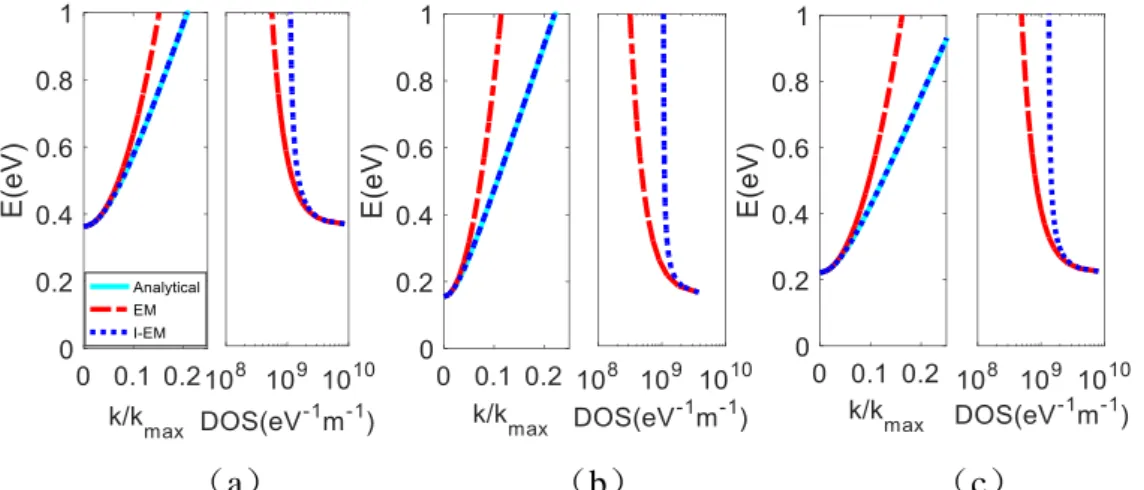
2 d d I d d 2 2 I d d 2 π 0 0 E k M D E E k E (1.30)While (1.25) is a less accurate approximation, it allows to compute in close-form the integral in the case of ohmic contacts, and for this reason it is used in [56]. It will be show in next chapter that, in the presence of mechanic deformation, the parabolic expression is not always suitable for the deformed energy bands. The higher-order approximation will be there preferred and the integral (1.25) will be performed numerically.
30 The importance of the definition of an effective mass is also related to the possibility to achieve a closed-form calculation for the transmittivity T(E) of a charge through a Schottky contact at the source-graphene and drain-graphene interfaces and the electronic densities of charges in the channel. The final formulas can be used in the following for the relevant computation of charges and currents [56]. WKB approximation (named after physicists Wentzel, Kramers, and Brillouin and developed as a general method of approximating solutions to linear, second-order differential equations) can be used to obtain closed-form transmission coefficients valid under deformation. The transmission coefficient calculated through WKB approximation [56] reads:
s
/ 2 ln s 0 2 ln 2 A z E M T E Ae
E dz
(1.31)where λ describes the potential distribution along the channel and depends on the device geometry, and 𝐴s is the height of Schottky barrier at the source (the same equation holds for the barrier at the drain). Let now 𝑒−𝑧 𝜆⁄ = 𝑡,
s
s 1 2 2 ln 2 A E t E E t M T A dt
(1.32) 2 2 arctan 2 2 2 s 2 2 s 2 2 2 4 s 2 1 2 E t A M t E M A M E E A t t M M M (1.33)
1 s 2 s 2 lnT E 4λ M As E 1 E tan A E A E E (1.34)After (1.26) is computed, the surface potential 𝜙𝑐 can be determined by enforcing the equality between the micro-model and the macro-model in Section 1.5:
31 𝑄𝑚𝑖𝑐𝑟𝑜(𝜙𝑐) = 𝑄𝑚𝑎𝑐𝑟𝑜(𝜙𝑐) (1.35) resulting in a nonlinear equation to be solved numerically.
Practically, the numerical solution of (1.35) ( ) f c Qmicro( )c Qmacro( )c 0 for the variable c is performed by applying the bisection method [57], described in Figure 1.14. One start looking for the solution in an arbitrary interval [c1_initial, c2 _initial] (in our case, we set c1_initial 2Vandc2 _initial 2V). We employ the continuity of the function ( )f c on the interval [ c1, c2] and we check if f(c1) and f(c2) have opposite signs. If
1_ 2 _
( c initial) ( c initial) 0
f f , no sign change is present in the interval [ c1, c2] (the presence of one zero at the most is assumed in the interval), and the initial interval is extended. Otherwise, one zero of f is present in the interval[ c1, c2]. The interval is divided in two and the procedure is repeated in each of the sub-intervals, until when the zero is found with a sufficient accuracy.
Figure 1.14: Illustration of the bisection method.
1.7 Research Objectives
1.7.1 Graphene nanoribbon based transistors
The electronic performance of graphene nanoribbon-based transistors is related with their geometric shape and working environment. In fact, strain operating on the flexible
32 substrate, and its subsequent deformation, could have a non-negligible impact on transistor performances (see Figure 1.15). Another interesting scenario where mechanical deformations could play a role is the use of transistors as bio-sensors [58]. The deformation of a graphene sheet would be related to the presence of a molecule to detect. For these reasons, we want to evaluate how the performance of graphene nanoribbon-based transistors will change when strains are applied on them.
Figure 1.15: (a) deformed graphene nanoribbon, (b) sectional view of a double-gate aGNR FET.
The effect of mechanical deformations on electrical properties of nano-transistors should be taken into account though their impact on the conducting properties of graphene. This can be done of course by means of ab-initio calculation, which are quite computational expensive. However, thanks to the lattice symmetries of graphene and the assumption of small deformations, closed-form results for the impact of deformation on the full energy bands of graphene can be derived. In fact, previous work has already been performed to show the effect of deformations on energetic properties of graphene sheets and nanoribbons [59]-[61], with both ab-initio formulations and other models. In [62] the electronic structure of graphene and graphene nanoribbons under strain is studied by using first-principles approaches and tight binding theory. In [63], a field-effect transistor (FET) under strains is studied with first-principle approaches.
However, engineering applications to practical circuits require a simple model, whose parameters can be directly related to relevant geometric quantities. For this reason, we aim at employing the semi-analytical approach [56] described in Section 1.4.2 to study the electronic characteristics of FET. The effect of mechanical strain on graphene-based nanotransistors has not been previously taken into account in this approach in the literature. For this purpose, in Chapter 2 we consider nanoribbon transistors under deformation: we rigorously take into
33 account the effect of the deformation on the energy bands of the graphene and on the electrostatic analysis of the complete device. This leads to a complete characterization of the device in terms of its current-voltage characteristics. If the deformation is assumed small, as is expected in nanodevices for flexible electronics, due to the small dimensions of the transistor with respect to the local curvature radius of the deformed substrate, its effect will be seen to result both in a spectral scaling of energy bands and a Dirac-point shift. Both effects are derived on the basis of ab-initio simulations and are subsequently considered in our method. This approach is capable to describe both ballistic and partially-ballistic conduction regimes.
1.7.2 Graphene nanomesh based transistors
Creating regular holes in the graphene sheet (the so-called nanomesh graphene) may be another choice to tune the bandgap [64]. The structure of graphene nanomesh is shown in Figure 1.16 and the characteristics of nanomesh devices were first discussed in [64]. The advantage of graphene nanomesh in FET is having a high ON/OFF current ratio and a saturated current at high drain voltage.
34 Electronic properties of graphene nanomesh have already been studied. In [67] the electronic properties of graphene nanomesh are computed by using first principle calculations, leading to the conclusion that zig-zag edged graphene nanomesh can be either semiconductors or semimetals according to their structure. In [68], the electronic, magnetic, and mechanical properties of graphene are studied by using a supercell method. The creation of a band gap due to quantum confinement in graphene nanomesh is discussed in [69], where a relationship between energy gap and hole arrangement is also given. Based on these previous studies of graphene nanomesh, in [70] the fabrication of graphene nanomesh whith ribbon width less than 10 nm is achieved (see Figure 1.17). The fabricated graphene nanomesh samples are used in FET and the relationship between the On/Off current ratio and ribbon-width is obtained, showing that the On/Off current ratio increases when the ribbon width is reduced.
Figure 1.17: Schematic illustration of graphene nanomesh ribbon width [70].
In Chapter 3, computation and measurement of the I-V characteristics of the graphene nanomesh transistors (see Figure 1.18) will be presented. We employ a semi-analytical compact approach based on the energy gap calculated with the ab-initio method. We compare the qualitative behavior of simulated devices with independent measurements performed on fabricated devices. We investigate the influence of mesh shape and of geometrical parameters on the conduction properties of the devices.
35 Figure 1.18: Nanomesh graphene transistor [70].
36
Chapter 2. Dispersion Relations under Deformation and
Schottky Field-Effect Transistor
In this chapter, a tight-binding model is used to describe the effect related to mechanical deformations of graphene nanoribbons on the performance of nano-transistors. We accordingly define modified effective masses and density of states which are necessary to be used in the description of graphene FET. Once electronic properties of graphene nanoribbons under strain are determined, the currents of the field effect transistor can be calculated.
Numerical results are presented in this Chapter for currents and potentials in a nanotransistor which channel is an aGNR strip with different widths, both in ballistic and in partially-ballistic regime. Both Ohmic contacts and Schottky barriers can be considered.
2.1 Energy bands of a deformed graphene nanoribbon
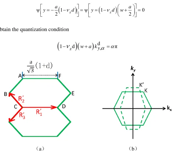
Equation (1.9) gives the energy bands of an aGNR in the absence of any geometrical deformation. In the presence of a relative deformation d, the values of the geometrical vectors
R1, R2, and R3 describing the relative position of atoms will change accordingly into 𝑹′𝟏,𝑹′𝟐
and 𝑹′𝟑 (the deformation is shown in Figure 2.1). Their values can be easily computed, thus
leading to a modified equation for 𝐸𝛼𝑑, the th energy band under deformation. The kx
dependence is then replaced in (1.9) into (1+d) kx. On the one hand, regarding the ky
dependence, the width w in (1.7)-(1.8) is deformed into 𝑤, = 𝑤(1 − 𝜈𝑔𝑑), where 𝜈𝑔 is the
Poisson’s ratio of the graphene, usually taken approximately equal to 0.145 [71]. The discretized values for ky are scaled accordingly as 𝑘𝑦,𝛼𝑑 = 𝑘𝑦,𝛼/(1 − 𝜈𝑔d) . The different
values of the mutual distances among atoms modify also the relevant hopping parameter. More specifically, different hopping parameters are now expected depending on the considered couple of atoms, due to the loss of hexagonal symmetry. If we do not consider any variation of hopping parameter in the tight-binding Hamitonian at this step, the argument of the cosines in the Aα would then be unchanged due to the multiplication between 𝑘𝑦,𝛼𝑑 and the
37 modified transverse dimension 𝑎(1 − 𝜈𝑔𝑑)/2. In fact, by enforcing a hard condition on the electronic wavefunction ψ
1
ψ
1
0 2 g g 2 a a y d y d w (2.1)we obtain the quantization condition
1
gd
wa k y
d, π (2.2)Figure 2.1: Deformation of Brillouin zone with the effect of strain (a) geometric effect of strain on graphene cell, (b) deformation of the Brillouin zone.
So that
2απ d , 1 1 g k y N a
d (2.3)The A factor in (1.9) becomes then:
2απ
1 1 cos 1 co co s 2 s 1 1 2 d g g y g N a d a d d a N A
k
(2.4)where the effect of deformation has no impact. The final energy bands of the nanoribbon deformed along the x dimension is then:
38
2d 3a d d d
1 4 cos 1 cos 1 4 cos 1
2 x g 2 y g 2 y a a E V d k d k d k k (2.5)
In (2.5), for convenience, 𝑘𝑥d will be abbreviated as k in the following:
d 3a 2 V 1 4 cos 1 4 2 k E k d A A (2.6)The band model (2.6) can be used together with a first-order correction δ𝐸𝛼′ , which is
based on a perturbative approach [72] taking into account a different interaction among the atoms at the edges, being at a different chemical potential with respect to the central ones, by slightly varying their mutual hopping integrals:
δ '
0.12Vsin2 π cos a 1
N 1 N 1 3
d k E k
(2.7)
The edge-corrected energy dispersion is then:
Ec
k Ed
k δE'
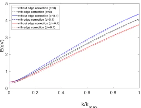
k (2.8)Figure 2.2: Comparison of the subbands of an aGNR with N=12 lines between tight-binding calculation with and without edge correction. (a) No deformation (b) Relative deformation
d=0.1 (c) Relative deformation d=-0.1.
The discussion presented for energy dispersion is summarized in Figure 2.2, with and without edge correction (2.7) for different values of the relative deformation d. The solid black line represents the numerical result without edge correction and the dashed red line represents the result with edge correction.
39
Figure 2.3: Comparison of the lowest subbands of an aGNR with 12 dimer lines with different deformations as explained in the legend.
An important limitation of (2.8) should be stressed: no energy-gap variation can be detected with this approach, as can be done with the first-principle formulations that will present next. This depends on the fact that the hopping integrals describing the interaction between two adjacent atoms have been kept constant even in the presence of a deformation. Therefore, we cannot see any change for energy gap in our simulation results as Figure 2.3 shows. In order to obtain more accurate results, the variation of hopping integrals under deformation should be taken into account, due to the presence of different distances among nearest-neighbor atoms [73]. When a symmetric strain is present, the Hamiltonian can be calculated with (1.2). If the strain applied is uniaxial, the hopping parameter depends on the bond lengths. In this case V1, V2, and V3 are no longer equal and the Fermi point will deviate
as Figure 2.1 shows.
The tight binding Hamiltonian is:
𝐻(𝒌) = 𝑉1𝑒−𝑗𝒌∙𝑹𝟏 + 𝑉
2𝑒−𝑗𝒌∙𝑹𝟐 + 𝑉3𝑒−𝑗𝒌∙𝑹𝟑 (2.9)
In case of small deformations, a perturbation method can be performed on the Hamiltonian around the Fermi point. In order to do this, we need an analytic expression for the variation of the hopping parameters V1, V2, and V3 with the respect to the deformation. A

![Figure 1.9: Comparison of ab-initio and NNTB model for energy dispersions calculation [12]](https://thumb-eu.123doks.com/thumbv2/123doknet/14527992.723143/18.892.270.615.111.364/figure-comparison-initio-nntb-model-energy-dispersions-calculation.webp)