HAL Id: hal-01694470
https://hal.archives-ouvertes.fr/hal-01694470
Submitted on 15 May 2018
HAL is a multi-disciplinary open access
archive for the deposit and dissemination of
sci-entific research documents, whether they are
pub-lished or not. The documents may come from
teaching and research institutions in France or
abroad, or from public or private research centers.
L’archive ouverte pluridisciplinaire HAL, est
destinée au dépôt et à la diffusion de documents
scientifiques de niveau recherche, publiés ou non,
émanant des établissements d’enseignement et de
recherche français ou étrangers, des laboratoires
publics ou privés.
Minibands modeling in strained balanced
InGaAs/GaAs/GaAsP cells
Benoit Galvani, Fabienne Michelini, Marc Bescond, Masakazu Sugiyama,
Jean-Francois Guillemoles, Nicolas Cavassilas
To cite this version:
Benoit Galvani, Fabienne Michelini, Marc Bescond, Masakazu Sugiyama, Jean-Francois Guillemoles,
et al.. Minibands modeling in strained balanced InGaAs/GaAs/GaAsP cells. Optoelectronics and
Photonic Materials and Devices Conference (SPIE OPTO), Jan 2017, San Francisco, CA, United
States. �10.1117/12.2252074�. �hal-01694470�
Minibands modeling in strained balanced
InGaAs/GaAs/GaAsP cells
Benoit Galvani
1, Fabienne Michelini
1, Marc Bescond
1, Masakazu Sugiyama
2,4,
Jean-François Guillemoles
3,4and Nicolas Cavassilas
11
Aix Marseille Université, CNRS, Université de Toulon, IM2NP UMR 7334, 13397,
Marseille, France
3
Department of Electrical Engineering and Information Systems, The University of Tokyo,
Tokyo, Japan
2
IRDEP, Institute of R&D on Photovoltaic Energy, UMR 7174,
CNRS-EDF-Chimie ParisTech, 6 Quai Watier-BP 49, 78401 Chatou Cedex, France
4
NextPV, LIA CNRS-RCAST/U. Tokyo-U. Bordeaux, 4-6-1 Komaba, Meguro-ku,
Tokyo 153-8904, Japan
ABSTRACT
In photovoltaic, multi quantum wells (MQW) allow to tailor the optical absorption. This is particularly interesting in multijunction solar cells [1] but it also permits to improve the efficiency of a single junction solar cell [2]. This approach is efficient thanks to the strain-balanced materials which, at a well under compressive strain, associates a barrier under tensile strain. This permits to consider a large number of wells while preventing the formation of dislocations during crystal growth.
On the other hand, the use of barriers is a drawback for the collection of the photo-generated carriers and more generally for the electronic transport quality in the MQW. Indeed, since transport is a succession of thermal escape, assisted tunnel escape and, at best, direct tunneling across a barrier, the average carrier velocity is low (of about 104 cm s-1) [3]. Finally the recombination rate is large and impacts both open-circuit voltage and short-circuit current.
Furthermore, thanks to barriers some minibands can occur [4]. The wave functions of carriers in minibands are Bloch waves, meaning that propagation is efficient. Our theoretical study, based on quantum simulation (Green functions formalism) in InGaAs/GaAs/GaAsP cells, sheds light on minibands in which the average velocity of carriers is around 107 cm s-1. However, we also show that, without an adapted design, such minibands are inefficient since they connect only a few wells. We will present some improvements related to the distance between barriers and the positioning of the MQW inside the cell.
Keywords: multi quantum wells, quantum modeling, minibands, carrier collection
1. INTRODUCTION
Over the last decades, carriers transport phenomena in semiconductor materials have been investigated to increase the performances of optoelectronic devices. The study was focused on properties of materials used in such devices. Then, Leo Esaki and Raphael Tsu have proposed in 1970 a theoretical study [5] of structures with periodic potential called superlattices (SL). They showed that SLs could exhibit remarkable optical and electronical properties, such as negative differential conductance and minibands. Even if the physical concepts predicted by Esaki and Tsu were controversial, the study of these quantum mechanical effects has opened a brand new research field in semiconductors. The development of epitaxial growth techniques has permit to fabricate SLs-based devices made of layers of a few nanometers, and thus to validate the theoretical models
experimentally. In 1986, Capasso et al. observed for the first time resonant tunneling in a AlInAs/GaInAs SL[6]. Miniband conduction was also investigated by Schneider et al. in a GaAs/AlAs structure[7]. Mendez et al. worked on Stark localization in GaAs/GaAlAs SLs to highlight the influence of an applied electric field on the miniband conduction[8]. During the early 1990’s, a lot more experiments[9, 10] were carried out to observe optical and electronical properties of SLs, even at room temperature [11]. Possible applications for these interesting properties were discussed[5, 10]. Capasso et al. observed sequential resonant tunneling in SLs that could be used for lasers and wavelength selective detectors[12]. Rudolf F. Kazarinov and Robert A. Suris suggest the possibility of using intersubbands transitions in a semiconductor device made of SLs[13] to achieve laser emission, which will lead to the creation of quantum cascade lasers. Most of SLs devices are light emitting devices such as lasers, where SLs dimensions and materials can be tuned to modify the band structure and thus to control the wavelength of emitted photons. Frequency modulators exploit the negative differential conductance property of semiconductor SLs to operate at high frequency. Solar cells can also benefit from the use of MQW structures to tailor the optical absorption [1, 2].
In this paper, we discuss the possibility of using minibands in SLs to improve the carrier transport in solar cells and thus to increase their efficiency. Our numerical study was carried out on a InGaAs/GaAs/GaAsP MQW nanostructure used in p-i-n single junction solar cells. We have implemented a numerical code using Green Function formalism [14] in order to calculate the band diagram of the whole structure and the corresponding local density of states (LDOS). We have studied the influence of SL layer widths on both minibands formation and carrier transport. We figured out that some structural optimizations can allow to extend both valence and conduction minibands across the whole MQW region, and thus to improve the transport and the collection of carriers.
2. THEORY OF MINIBANDS FORMATION
Before showing our results, we will briefly explain the physical processes behind minibands formation in SLs. Let’s consider a periodic SL made of N periods with two different semi-conductor materials A and B. The energy gap difference between A and B will form a barrier/well potential configuration. The Hamiltonian of this system can be written using an N-by-N matrix representation shown below :
where E1 represents the eigenvalue of the fundamental energy level for an isolated well and V represents the tunnel coupling terms between wells (hopping). We consider in this case nearest-neighbor interactions only. It have been demonstrated that the E(k) dispersion relation of electrons in this system is a sinusoidal function in the form:
In this equation, k is the wave vector and a is the SL period. The dispersion relation of this system defines allowed energy states called miniband. This phenomenon will modify the carrier transport properties of the SL since electrons (and holes) are delocalized in the whole region crossed by the miniband. From Eq. (2), we can calculate the effective mass of electrons in the miniband :
(1)
The effective mass depends on the SL period a and on the hopping term V. The average velocity can also be obtained from :
Minibands in SL could potentially increase the current generated by the cell. Indeed, if a carrier reaches one of the energy states composing the miniband, it will be completely delocalized along the whole structure, meaning that such carriers propagate with an average velocity which can be high.
3. STRUCTURE AND PARAMETERS
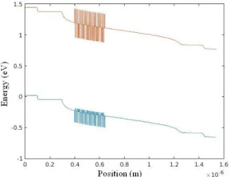
The MQW region of the studied solar cell is an undoped InGaAs/GaAs/GaAsP SL (20 periods) made of alternation of 22 Å GaAs0.58P0.42 barrier, 38 Å In0.21Ga0.79As well and two 31 Å GaAs interlayers between each barrier and well. The SL is sandwiched between two undoped GaAs layers, with an adapted thickness to get a total undoped region (GaAs layers + SL) of 1µm. GaAs interlayers helps to reduce lattice relaxation during epitaxial growth[15]. The whole calculated band diagram is shown in Fig. 1. Self-consistent calculations were made by resolving Schrödinger-Poisson equations using Green function formalism. This way permits to assume quantum properties of electronic transport such as tunneling, interference, and confinement.
The energy band gaps of each material with such compositions are 1.42 eV for GaAs, 1.99 eV for GaAsP and 1.13 eV for InGaAs. The effective masses of electrons are equal to 0.067 m0 for GaAs, 0.1102 m0 for GaAsP and 0.0585 m0 for InGaAs, where m0 is the free electron mass [16]. However, in strained materials, the band structure will be modified, which will lead to some differences in the values of energy gaps and effective masses. In order to use the correct values as entry parameters, we have calculated the band structure of each strained material (InGaAs and GaAsP in our system) using a 8-band k.p model. Calculated energy gaps in strained materials are equal to 1.87 eV and 1.15 eV for GaAsP and InGaAs respectively. Effective masses of electrons were also calculated and are equal to 0.097 m0 and 0.068 m0 for GaAsP and InGaAs respectively.
Fig. 1: Band diagram of the modeled solar cell. The SL region is made of alternation of 22 Å GaAs0.58P0.42 barrier, 38 Å
In0.21Ga0.79As well and 31 Å GaAs interlayers between each barrier and well. Red lines represent the CB and blue lines
represent the VB.
(3)
4. MINIBAND WITHOUT ELECTRIC FIELD
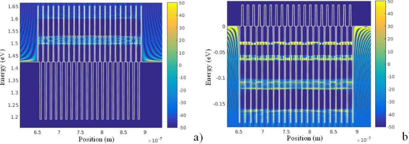
For a first calculation, we assume no electric field in order to extract the minibands parameters. Our numerical LDOS calculations for a 20-period SL as defined above are shown in Fig. 2 as a function of the energy and the position in the transport direction. LDOS shows minibands in the GaAsP barriers in both conduction band (CB) and valence band (VB). Such minibands are extended across the whole MQW region. We note that the miniband in CB is made of second-order energy states. The first-order energy states are located deeper inside the well, but they are not visible here. Indeed, in this calculation, we do not assume inelastic behavior such as electron-phonon or electron-photon scatterings. In this case, states in the QWs are no coupled to the contacts, and the corresponding LDOS is not visible [17,18].
For the minibands, which are directly coupled to the contacts, the effective masses for CB and VB calculated with Eq. (3) are equal to 0.029 m0 and 0.173 m0 respectively. These results show that both electrons and holes have effective masses lower than those in a bulk GaAs material, which are equal to 0.063 m0 for electrons and 0.51 m0 for holes. Average velocities calculated from Eq. (4) are equal to 3.22 107 cm/s for electrons and 5.52 106 cm/s for holes. These velocities are much higher than velocities in a SL without minibands, estimated to be 2.1 104 cm/s for both electrons and holes [3], since electronic transport is a succession of thermal escape, assisted tunnel escape and direct tunneling across barriers. For this SL, ballistic escape time for electrons and holes are estimated to be 7.58 10-13 s and 4.42 10-12 srespectively. Since miniband are narrower than the optical phonon energy (ħω=35 meV) the ballistic behavior is expected to be significant.
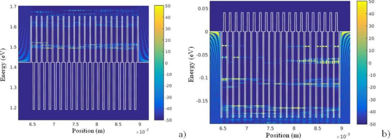
Our numerical study was made considering a perfectly periodic system with fixed layer widths. However, in a realistic system, layer widths are controlled during the epitaxial growth in order to balance strains in order to avoid dislocations. This leads to induce some small variations in each layer width depending on the strains within the structure and the minimum width that can be grown. In order to take such variations into account, we modeled the same system as shown above, but we added a +0.2, 0 or -0.2nm on each layer width. Variations are randomly chosen for each layer. Fig. 3, which represents the corresponding LDOS, shows that minibands in both CB and VB are not perfectly formed. This is due to the fact that the SL periodicity is altered. In order to demonstrate the importance of the periodicity, we also assumed the randomly generated structure, but with GaAs interlayers widths adjusted in order to keep the SL periodicity. Fig. 4 shows the LDOS calculations for this structure. This system exhibits extended minibands in both CB and VB, which prove that periodicity is a key factor to have extended minibands.
Fig. 2: LDOS of the MQW region of an undoped InGaAs/GaAs/GaAsP 20-period superlattice made of alternation of 22 Å GaAs0.58P0.42 barrier, 38 Å In0.21Ga0.79As well and 31 Å GaAs interlayers. The LDOS (color scale on the right) is calculated in
Fig. 3: LDOS of the MQW region of an undoped InGaAs/GaAs/GaAsP 20-period superlattice with randomly generated errors on each layer width. Errors can be equal to +0.2, +0 or -0.2nm for each layer. The LDOS (color scale on the right) is calculated in arbitrary units, as a function of the energy and the position. a) LDOS calculated in CB. b) LDOS calculated in VB.
Fig. 4: LDOS of the MQW region of an undoped InGaAs/GaAs/GaAsP 20-period superlattice with randomly generated errors on each barrier and well width, and with recalculated interlayer widths to maintain SL periodicity. Errors can be equal to +0.2, +0 or -0.2nm for each layer. The LDOS (color scale on the right) is calculated in arbitrary units, as a function of the energy and the position. a) LDOS calculated in CB. b) LDOS calculated in VB.
5. CALCULATIONS IN THE SOLAR CELL
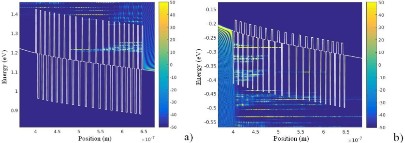
In a SL without any external electric field, this miniband extends across the whole MQW region. However, in a solar cell electric field is required and the LDOS within the MQW region change as well. Fig. 5 shows the LDOS calculations for the 20-period GaAs0.58P0.42/GaAs/In0.21Ga0.79As solar cell under a 0.75 V applied bias. The LDOS in CB for this solar cell exhibits a miniband that cross around 13 wells of the SL. Indeed, the electric field tends to shift the energy states in each quantum well, and so, the coupling between wells is not strong enough to allow tunneling process across the whole quantum well region. We note that the second-order miniband in VB is almost not visible.
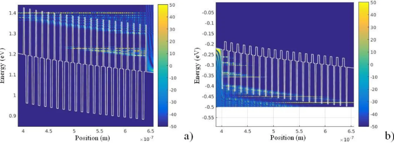
In order to expand miniband across the whole MQW region, we have modeled a 20-period SL with the GaAs interlayer widths increasing from the n-side to the p-side following a quadratic gradient. The quadratic evolution of the interlayer width permits to align correctly the energy level since the energy states in a quantum well are function of the squared value of the well width. Fig. 6 shows the LDOS calculations under a 0.75 V external bias with interlayer width increasing from 48 Å to 84 Å. The initial value of the interlayer width is higher than the value in the original solar cell (31 Å) to see the evolution of the miniband energy.
In this configuration, the second-order miniband is lower in energy due to the larger interlayer widths. Moreover, the system exhibits a third-order miniband that crosses 18 periods. In this case, more periods are coupled to the contacts. However, there is no miniband in VB. Indeed, if the interlayer width gradient is adapted to expand the miniband in the CB, it is the opposite in VB. This simple gradient is thus adapted either to the CB or the VB. However it can be interested for the collection of carrier generated in the GaAs. If, as shown in Fig. 1 the MQW are located near to the p-doped side of the solar cell, it could be interesting to have an extended miniband in VB, in order to make the holes transport more efficient.
Fig. 5: LDOS of the MQW region of an undoped InGaAs/GaAs/GaAsP 20-period superlattice under a 0.75V external bias. The LDOS (color scale on the right) is calculated in arbitrary units, as a function of the energy and the position. a) LDOS
calculated in CB. b) LDOS calculated in VB.
Fig. 6: LDOS of the MQW region of an undoped InGaAs/GaAs/GaAsP 20-period superlattice under a 0.75V external bias with an interlayer width gradient from 84 Å to 48 Å. The LDOS (color scale on the right) is calculated in arbitrary units, as a function of the energy and the position. a) LDOS calculated in CB. b) LDOS calculated in VB.
In order to expand both CB and VB minibands, we have assumed a double quadratic evolution of the interlayer widths. The interlayer width increases from the p-side to the middle of the SL, and then it decreases from the middle of the SL to the n-side of the solar cell. Fig. 7 shows the LDOS calculated for the double gradient with, from p-side to the middle of the SL to the n-side, 22/53/22 Å interlayers. The solar cell exhibits CB and VB minibands, expanded across 13 and 9 periods respectively.
Fig. 7: LDOS of the MQW region of an undoped InGaAs/GaAs/GaAsP 20-period superlattice under a 0.75V external bias with an interlayer width (22/53/22Å) double gradient. The LDOS (color scale on the right) is calculated in arbitrary units, as a function of the energy and the position. a) LDOS calculated in CB. b) LDOS calculated in VB.
6. CONCLUSION
In this paper, we have shown that miniband engineering could help to increase the efficiency of solar cells. Carriers in minibands have lower effective masses than their bulk counterparts. The average velocity of carriers in the miniband is higher than in bulk and strongly higher than a SL without miniband.
We have made LDOS calculations using Green function formalism to show the evidence of miniband formation in a 20-period GaAs0.58P0.42/GaAs/In0.21Ga0.79As SL without any electric field in the active region. We showed the importance of the system periodicity on the miniband formation phenomenon.
LDOS calculations for the same solar cell under a 0.75 V applied bias showed that the valence miniband is not expanded across the MQW region, and thus because the internal electric field tends to shift the energy states, reducing the coupling between periods.
Finally, we have proposed a solution to expand both conduction and valence miniband across the SL. By using an interlayer width gradient, we can improve the coupling between more periods of the system and so permit to expand the miniband. However, in order to achieve both conduction and valence miniband improvements, an interlayer width double gradient is needed.
REFERENCES
[1] Browne, B., Lacey, J., Tibbits, T., Bacchin, G., Wu, T.-C., Liu, J. Q., Chen, X., Rees, V., Tsai, J., et al., “Triple-junction quantum-well solar cells in commercial production,” AIP Conference Proceedings 1556(1), 3-5 (2013).
[2] Adams, J. G. J., Browne, B. C., Ballard, I. M., Connolly, J. P., Chan, N. L. A., Ioannides, A., Elder, W.,Stavrinou, P. N., Barnham, K. W. J., et al., “Recent results for single-junction and tandem quantum well solar cells,” Prog. Photovolt: Res. Appl. 19(7), 865–877 (2011).
[3] Toprasertpong, K., Tanibuchi, T., Fujii, H., Kada, T., Asahi, S., Watanabe, K., Sugiyama, M., Kita, T. and Nakano, Y., “Comparison of Electron and Hole Mobilities in Multiple-Quantum-Well Solar Cells Using a Time-of-Flight Technique,” IEEE Journal of Photovoltaics, 5(6), 1-8 (2015).
[4] Usuki, T., Matsuochi, K., Nakamura, T., Toprasertpong, K., Fukuyama, A., Sugiyama, M., Nakano, Y., Ikari, T., “Observation of mini-band formation in the ground and high-energy electronic states of superlattice solar cells,” Proc. SPIE 9743, 974312 (2016).
[5] Esaki, L., Tsu, R., “Superlattice and Negative Differential Conductivity in semiconductors,” IBM J. Res. Develop. 14 (1), 61-65 (1970).
[6] F. Capasso, K. Mohammed and A.Y. Cho, “Sequential resonant tunneling through a multiquantum well superlattice,” Appl. Phys. Lett. 48 (7), 478-480 (1986).
[7] Schneider, H., Grahn, H. T., von Klitzing, K., “Tunneling resonances and miniband conduction in superlattices,” Surface Science, 228 (1–3), 362-369 (1989).
[8] Mendez, E. E., Agullo-Rueda, F. and Hong, J. M., “Stark Localization in GaAs-GaAlAs Superlattices under an Electric Field,” Phys. Rev. Lett., 60(23), 2426-2429 (1988).
[9] Sibille, A., Palmier, J.F., Hadjazi, M., Wang, H., Etemadi, G., Dutisseuil, E., Mollot, F., “Limits of semiclassical transport in narrow miniband GaAs/AlAs superlattices,” Superlattices and microstructures, 13(2), 247-253 (1993).
[10] Mendez, E. E., Bastard, G., “Wannier-Stark Ladders and Bloch Oscillations in Superlattices,” Physics Today, 46(6), 34-42 (1993).
[11] Dekorsy, T., Ott, R., Kurz, H., Kohler, K., “Bloch oscillations at room temperature,” Phys. Rev. B, 51(23) 17275-17278 (1995).
[12] Capasso, F., Mohammed, K., Cho, A.Y.,” Resonant Tunneling Through Double Barriers, Perpendicular Quantum Transport Phenomena in Superlattices, and Their Device Applications,” IEEE J. Quantum Electron. 22(9), 1853-1869 (1986).
[13] Kazarinov, R. F., Suris, R. A., “Possibility of the amplification of electromagnetic waves in a semiconductor with a superlattice,” Soviet Physics – Semiconductors, 5(4), 797-800 (1971).
[14] Cavassilas, N., Michelini, F., Bescond M., “Modeling of nanoscale solar cells: The Green's function formalism,” J. Renewable Sustainable Energy 6, 011203 (2014).
[15] Fujii, H., Toprasertpong, K., Wang, Y., Watanabe, K., Sugiyama, M., Nakano, Y., “100-period, 1.23-eV bandgap InGaAs/GaAsP quantum wells for high-efficiency GaAs solar cells : toward current-matched Ge-based tandem cells,” Prog. Photovolt: Res. Appl, 22(7), 784-795 (2014).
[16] Vurgaftman, I., Meyer, J. R., Ram-Mohan, L. R., “Band parameters for III–V compound semiconductors and their alloys,” J. of Appl. Phys., 89(11), 5816-5874 (2001).
[17] The first order states in InGaAs quantum wells are below the GaAs conduction band. Without any inelastic scattering electrons on such a state has thus an infinite life time. By the uncertainty principle, the state is then no broaden (Dirac function) and then cannot be represented on an energy mesh.
[18] Cavassilas, N., Michelini, F., Bescond M., “Theoretical comparison of multiple quantum wells and thick-layer designs in InGaN/GaN solar cells,” Appl. Phys. Lett. 105, 063903 (2014).