HAL Id: hal-02319457
https://hal.laas.fr/hal-02319457
Submitted on 18 Oct 2019
HAL is a multi-disciplinary open access
archive for the deposit and dissemination of
sci-entific research documents, whether they are
pub-lished or not. The documents may come from
teaching and research institutions in France or
abroad, or from public or private research centers.
L’archive ouverte pluridisciplinaire HAL, est
destinée au dépôt et à la diffusion de documents
scientifiques de niveau recherche, publiés ou non,
émanant des établissements d’enseignement et de
recherche français ou étrangers, des laboratoires
publics ou privés.
New defect detection approach using near
electromagnetic field probing for high density PCBAs
New defect detection approach using near
electromagnetic field probing of high density PCBAs
Nabil El Belghiti Alaoui, Patrick Tounsi, Alexandre Boyer, Arnaud Viard
To cite this version:
Nabil El Belghiti Alaoui, Patrick Tounsi, Alexandre Boyer, Arnaud Viard. New defect detection
approach using near electromagnetic field probing for high density PCBAs New defect detection
ap-proach using near electromagnetic field probing of high density PCBAs. 29 th European Symposium
on Reliability of Electron Devices, Failure Physics and Analysis (ESREF 2018), Oct 2018, Aalborg,
Denmark. �10.1016/j.microrel.2018.07.090�. �hal-02319457�
New defect detection approach using near electromagnetic field
probing for high density PCBAs
N. El-Belghiti Alaoui
a,b,*, P. Tounsi
a, A. Boyer
a, A. Viard
ba Laboratoire LAAS-CNRS, Institut National des Sciences Appliquées, France b ACTIA Automotive, 5 Rue Jorge Semprun, 31400, France
Abstract
With the density increase of today’s printed circuit board assemblies (PCBA), the electronic fault detection methods reached their limits, in the same time the requirements of high reliability and robustness are greater. Industrials are obliged to reduce the number of physical test points and to find better-adapted test methods. Current test methods must be rethought to include a large panel of physical phenomena that can be used to detect electrical defects of components, absence, wrong value, and shorts at component level on the board under test (BUT).
We will present the possibility of using electromagnetic signature to diagnose faulty components contactlessly. The technic consists in using small diameter near electromagnetic field probes which detect the field distribution over powered sensitive components. The biasing of the BUT is specifically chosen to enhance the sensitivity of the EM measurements. Reference EM signatures are extracted from a fault-free circuit, which will be compared to those extracted from a sample PCBA in which we introduced a component level defect by shorting, removing or changing the value of critical components. As a result, we will show that the amplitude of a specific harmonic acts as a sensing parameter, which is accurately related to the variation of the component value.
Preferred presentation: [ ] Oral
[ ] Poster [x] No preference
Preferred track (please, tick one or number 1 to 3 tracks in order of preference: 1 = most suiting, 3 = least suiting) [2] A - Quality and Reliability Assessment Techniques and Methods for Devices and Systems
[ ] B1 - Si Technologies & Nanoelectronics: Hot Carriers, High K, Gate Materials [ ] B2 - Si Technologies & Nanoelectronics: Low K, Cu Interconnects
[ ] B3 - Si Technologies & Nanoelectronics: ESD, Latch-up [1] C - Progress in Failure Analysis: Defect Detection and Analysis [ ] D - Reliability of Microwave and Compound Semiconductors Devices [3] F - Packaging and Assembly Reliability
* Corresponding author
New defect detection approach using near electromagnetic field
probing of high density PCBAs
N. El-Belghiti Alaoui
a,b,*, P. Tounsi
a, A. Boyer
a, A. Viard
b1. Introduction
During the assembly process of printed circuit boards, defects such as wrong value components, missing components, unwanted open circuits or short circuits may appear. Manufacturers continually look for faster, more accurate and more economical ways to identify this kind of defects. That’s why performing automated testing of dense populated printed circuit boards is a mandatory and cost effective solution to ensure manufacturing quality control.
Defect detection in today’s populated PCBs is becoming increasingly challenging and more expensive as the use of small size surface mounted devices (SMD) is becoming predominant. The emergence of new technologies as High-Density Interconnect (HDI), embedded chips and Sequential Build-Up (SBU) circuit boards will even further increase the challenge for the test business.
Starting from this need, the idea of contactless defect detection on PCBs to meet the current challenges have come.
In this paper, we present a new defect detection approach using EM near field probes over components on populated PCBs.
After a presentation of the state of the art, the principle of the proposed method is given in order to understand its large scale application. To this aim and to prove the effectiveness of the method, we chose a DC/DC buck converter module as a case study. Simulations of value defect scenarios have been carried out on Cadence Orcad and validated by measurements on the module in which we introduced controlled value defects on the input decoupling ceramic capacitors. First results to validate the principle and perspectives for future work are reported.
2. State of art
Many research activities have been conducted to complement the actual PCB defect detection technics and eliminate its drawbacks. Probing techniques [1,2,3] and inspection methods [4,5,6] have been
imagined by many researchers over the last 30 years. However, despite its immense ingenuity, they could not respond completely to the access constraints of high density PCBAs and pinpoint exactly where the defective component is located.
3. Description of the proposed testing approach
To improve the effectiveness and accessibility to components that could not be tested without placing numerous test points, we propose in this article a new defect detection approach based on EM inspection using near field probes. With near field measurements above PCBA components, contactless information about charge and current distribution can be obtained without access limitation on the PCBA surface.
3.1. Principle
The principle of this method is to measure the EM near field distribution directly over the center of a powered component contactlessly and compare the measured electromagnetic signature (EMS) to a database of correct signatures pre-established on a fault-free PCBA. The measured electric and magnetic fields (EMF) are generated by the distribution of charges and currents respectively in the components of the BUT. Accurate and repeatable measurements of these fields produce a specific time and frequency domain signature for each critical component, which can be extended to a complete operational block, and then to the complete board in a further application. Such signatures are then compared to a pre-established non-faulty signature pattern of the same type of board to determine whether the BUT is faulty or not and pinpoint exactly where the faulty component is located knowing the position of the near field sensing probe (NFP) on the board.
Thus firstly, the board or the operational block of the board is powered and operates normally. The electromagnetic near-field distribution generated by every “critical” component on the block is then detected using non-contact NFPs mounted directly
over these components in a bed-of-nails structure. The registered signature specific to the component and the conditions of the excitation of the electronic block is registered and subsequently compared with a sample signature of the same block in a non-faulty board, which was registered in the same excitation conditions to determine whether the response is in conformance with the known reference.
3.2. Types of assembly defects detected
The defects that can be detected with this method are defects on a component level. In other words, starting from the hypothesis that the bare PCB is fault free guaranteed from the printed circuit manufacturer, or had already been tested and certified non-faulty. We can detect defects over critical components: presence, polarity for components that exhibits field change when mounted in reverse polarizations, value, a wrong package that can change the height of the component, overstressed/overheating components and solder defect (open and shorts). These components must be carefully chosen in advance in order to establish design for test rules to minimize the probe count and maximize fault detection on a functional block level.
4. Study case: DC/DC buck converter
To validate our approach, we chose a DC/DC converter because of the important transient currents crossing the critical components when the module is powered. Components such as input/output filtering capacitors, MOSFETS and inductors radiate a significant magnetic field in the near field region due to the large transient currents crossing them. The currents and the induced magnetic fields are related to component values. From the analysis of measured magnetic fields, the presence and the location of assembly defects or wrong components can be detected.
This case represents a scenario of testing a DC/DC module in a power management block of an industrial high density PCBA using the EMF radiated from its critical components. Using a commercial near field probe, the EM signature of each of the critical components as described above is registered to establish a sample signature of each component.
We chose an off-the shelf (OTS) evaluation board of a synchronous DC/DC buck converter module with a fully integrated controller to run tests. The powering conditions for test are as mentioned in Table 1.
4.1. Simulated defect scenarios:
The first defect scenario used to validate this approach is the detection of a wrong value of an input decoupling capacitor. The approach is tested initially in simulation, and then validated in measurement.
4.1.1. Test procedure: Simulation
We modeled the DC/DC evaluation board on
Cadence-Orcad using the pspice model of the
controller given by the manufacturer. Estimated values of parasitic elements of each critical component were used to give a more accurate and “realistic” simulation results. Then, we ran multiple parametric simulations of the value of each input capacitor for four different values (see Table 2) to evaluate how the derivative of the current in each input capacitor reacting to a change of value of an input capacitor and the induced variation over the
other capacitors that have correct values. The derivative of the current in a component
represents the image of the magnetic field measured with a commercial NFP over this specific component.
4.1.2. Test procedure: Experimentation
We reproduced the same scenario described in the test procedure simulation with the same values on the evaluation DC/DC module. We changed the value of each input capacitor on the board several times by soldering and removing a different value capacitor for every input ceramic capacitor (C8,C9,C10,C11), and we collected the time domain signatures over each
Table 1
Powering conditions for test Vin 20 V
Vout 12 V
ILoad 3 A
Frequency 250 kHz
Table 2.
Values used for input capacitors in simulation and experiments Input capacitors Correct value (µF) Incorrect values (µF) C8 2.2µF 1, 1.5, 3.3, 15 C9 2.2µF 1, 1.5, 3.3, 15 C10 2.2µF 1, 1.5, 3.3, 15 C11 2.2µF 1, 1.5, 3.3, 15 C22 47µF unchanged
capacitor using an oscilloscope for each of the four values evaluated. Collected signatures of each capacitor were analyzed to evaluate their variance compared to the reference signatures.
4.1.3. Test bench description
Measuring the time domain H-field signatures over the energized (see Table 1) DC/DC buck-converter was carried out using a commercial mini (resolution <1mm) Near-Field probe (LANGER RF-R
0.3-3) (see Fig.1.b). The probe was directly connected
to a digital oscilloscope with 50Ω impedance and The NFP was then freely and accurately moved over every input capacitor at a 2mm distance of the center of the component using an automatic computer controlled scan table with a distance precision of 25µm (see Fig.1.a).
5. Simulation (vs) experimental results: 5.1. Reference signatures:
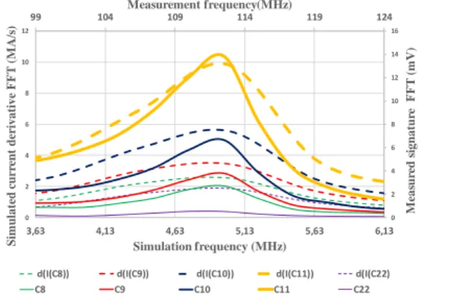
The reference signature is the EMF measured over each input capacitor when it has a correct value. Figure 2 shows a great coherence between the simulation results and the measurement results over input capacitors C8, C9, C10, and C11. The difference in the frequency scale is due to assumptions made on the parasitic parameters of the components in the simulation model to be considered in the future work. The difference of amplitudes between simulation and measurement is due to the coupling parameter of
the NFP that wasn’t taken into account in the simulation model.
5.2. Signatures with wrong values of the input capacitors:
In concerns of conciseness, only the signatures measured over all input capacitors induced from the variation of the value of the input capacitor C8 will be presented in this section (see Fig.3 and Fig.4). Details on the other test scenarios will be included in the complete article submission.
The dashed lines shows the small signature variations of the unchanged input capacitors (C9, C10, C11, C22). Bold lines are the variation of C8 signatures when we varied its value. Results from simulation and measurements shows that C8 EM signature varies significantly, while the other capacitors signature stays roughly unchanged.
Fig.1.a Test bench set-up
Precision automated scaning arm EM near field probe DC/DC buck converter board
Fig.1.b Close-up showing the NFP and the probed components
Distance=2mm
Tested input capacitors NFP
Fig.2 Simulated current derivatives FFT of input capacitors (dashed lines), (vs) measured EM signatures FFT on the
buck converter PCB 99 104 109 114 119 124 0 2 4 6 8 10 12 14 16 0 2 4 6 8 10 12 3,63 4,13 4,63 5,13 5,63 6,13 Measurement frequency(MHz) M eas u re d s ign at u re F F T ( m V ) S im u lat ed c u rr en t d er ivat ive F F T ( M A /s ) Simulation frequency (MHz)
d(I(C8)) d(I(C9)) d(I(C10)) d(I(C11)) d(I(C22)
C8 C9 C10 C11 C22
Fig.3 Simulated current derivatives FFT of input capacitors when C8 varies Variation of C8 value C8 reference signature C11 C10 C9 C22
5.3. Comparison and analysis:
From the measurement results we can see that the capacitor value change induces a significant variation on the amplitude spectrum at around 110MHz of the EM signature of the capacitor being changed.
This is still true for all capacitors when we change their value. They all exhibit a significant variance of their spectrum amplitude signature at around 110MHz.
These results can be summarized in the graph below (see Fig.5) which shows that the most scattered signatures around the reference are those of the decoupling capacitor for which the value was changed. The dispersion of signatures remains lower for all fixed capacitors.
6. Conclusion and future work:
We presented the possibility of using electromagnetic signature to diagnose faulty components contactlessly on a limited physical
access PCBA.
To validate the principle we used miniature near electromagnetic field probes to measure field distributions over powered sensitive components and to give insight on the value of the component and its solder condition (shorted, soldered or non-soldered). The biasing of the BUT was specifically chosen to enhance the sensitivity of the EM measurements. A proper amplification and signal conditioning will be considered to increase measurement sensitivity.
First raw measurement results showed that the amplitude of a specific harmonic on the spectral signature acts as a sensing parameter, accurately related to the variation of the component value.
Experiments are still going to validate the approach on large scale applications and results on fault detection in the output filter components and low frequency components will be presented in the full paper.
7. References
[1] K. P. Parker, “A new probing technique for high-speed/high-density printed circuit boards,” in Test Conference, 2005. Proceedings. ITC 2005. IEEE International, 2005, p. 10–pp.
[2] C.Vaucher and L. Balme, “Analog/digital testing of loaded boards without dedicated test points,” in Proceedings International Test Conference 1996. Test and Design Validity, 1996, pp. 325–332.
[3] Test access component for automatic testing of circuit assemblies, A.J.Suto, US patent application 20100207651
[4] H. Moldovan, M. Marcu, and M. Vladutiu, “PCB Testing Using Infrared Thermal Signatures,” in 2005 IEEE Instrumentationand Measurement Technology Conference Proceedings, 2005, vol. 3, pp. 1970–1974.
[5] Method for testing printed and unprinted circuit board assemblies aligning a focused, high-frequency electromagnetic transmission beam to irradiate a component to be tested and produce a spectral measuring signal, R.Wein, DE19837169A1
[6] Method and apparatus for high-speed scanning of electromagnetic emission levels,G.Gunthorpe & D.James, WO1997017617A1
Fig.4 Measured EM signatures FFT of the input capacitors when C8 varies
C8 reference signature C11 C10 C9 C22 Variation of C8 value
Fig.5 standard deviation of the measured amplitude spectrum EM signature in each case where the value of one
input capacitor is changed separately
x10 The value of this deviation is 2mV, it was divided by