HAL Id: hal-02066160
https://hal.laas.fr/hal-02066160
Submitted on 13 Mar 2019
HAL is a multi-disciplinary open access
archive for the deposit and dissemination of sci-entific research documents, whether they are pub-lished or not. The documents may come from teaching and research institutions in France or abroad, or from public or private research centers.
L’archive ouverte pluridisciplinaire HAL, est destinée au dépôt et à la diffusion de documents scientifiques de niveau recherche, publiés ou non, émanant des établissements d’enseignement et de recherche français ou étrangers, des laboratoires publics ou privés.
Flexible technology for millimeter-wave wireless sensors
applications
Alexandru Takacs, Daniela Dragomirescu, Samuel Charlot, Pierre-François
Calmon
To cite this version:
Alexandru Takacs, Daniela Dragomirescu, Samuel Charlot, Pierre-François Calmon. Flexible technol-ogy for millimeter-wave wireless sensors applications. IEEE International Workshop of Electronics, Control, Measurement, Signals and their Application to Mechatronics (ECMSM), May 2017, San Sebastian, Spain. pp.303-306. �hal-02066160�
Flexible technology for millimeter-wave wireless
sensors applications
A. Takacs1, D. Dragomirescu1, S. Charlot1, P-F Calmon1,
1 LAAS-CNRS, Université de Toulouse, CNRS, INSA, UPS, Toulouse, France
[email protected], [email protected], [email protected], [email protected]
Abstract—This paper addresses recent advances obtained in
LAAS CNRS concerning the developments of the flexible kapton technology and the use of this technology in the manufacturing of flexible and conformal structures for applications like Wireless Sensor Networks (WSNs) and Structure Health Monitoring (SHM). Flexible kapton supported passive devices are presented as well as the technological process developed for the heterogeneous integration of active circuits with such flexible passive devices.
Keywords—flexible electronics; wireless sensors networks, kapton
I. INTRODUCTION
The developments of any successful complex industrial product in the field of aeronautics, space, automotive or IoT industries requires the use of a huge numbers of sensors deployed both on the final product or on the prototypes used during the development cycle. These sensors should be low-cost, low-weight and deployed on various surfaces. In order to deploy a large number of such sensors in a conformal manner on irregular surface a flexible substrate is required. Many flexible substrate technologies are today available [1]-[2] and we focused our research on the kapton flexible substrates that offers a best trade-off between mechanical, thermal and electrical properties [3].
II. FLEXIBLE KAPTON TECHNOLOGY
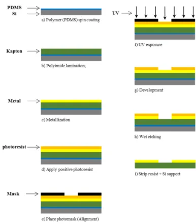
To manufacture our circuits onto a flexible substrate, we have chosen the traditional photolithography mainly because of the intrinsic high resolution [4]. The main difficulty during the fabrication process lies on the flexible film handling and its use in micro-technology equipment. In order to overcome this difficulty, a 4-inch silicon wafer is used as a host carrier. One of the critical obstacles consists of finding a way to adhere the polyimide film on the Si support. This adhesion has to be compatible with the various technological stages (vacuum, solvent and temperature) and allows after manufacturing a peeling without any physical or chemical constraint. A matured fabrication process was used and a PDMS (PolyDiMethylSiloxane) spin coating was performed for the adhesion of the polyimide on the holding wafer. Then the Kapton polyimide was patterned on the PDMS-Si support using a Shipley 360N laminator. A resin spin coating was then realized in a fully automated resist processing tool (EVG120),
followed by a photolithography process. During the different fabrication processes, Kapton polyimide was metallized with Ti/Au layers (50 nm/ 200 nm) or Ti/Cu layers (50 nm/500 nm) using the Electron Beam Physical Vapor Deposition (EBPVD). In case of Cu coating, the fabrication process was terminated with a surface finishing (gold immersion deposits) to prevent Cu from oxidizing. Both wet-etching (Fig. 1) and lift-off methods (Fig. 2) can be used [4], each of them allowing sufficient resolution (the minimum resolution is in the range of 1µm both the metallic strips and slot) for the metallization tracks for millimeter wave applications (up to W-band). The quality (homogeneity and roughness) of the metallization layers obtained by the adopted photolithography based technology are also better as compared with other flexible technology (e.g. inkjet printing).
Fig. 2. Main technological steps of the lift-off process
α + β = χ. (1) (1) III. DESIGN OF PASSIVE KAPTON COMPONETS FOR MILLIMETER
WAVE APPLICATIONS
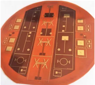
In order to validate our technological approach a lot of passive components were designed, fabricated and manufactured in our laboratory [4]-[6]. A thickness of 125 µm was selected for the Kapton film as a best trade-off between: (i) the commercially available thickness of Kapton films, (ii) the electromagnetic performances required by typical antennas (e.g. patch antennas) that can be used for millimeter wave applications, (iii) the mechanical properties. Fig. 3 shows a 4 inch kapton wafer including: (i) circular ring resonators (CRR), (ii) cross dipole antennas (by using strip or slot based topologies), (iii) patch antennas, (iv) rectennas (an acronym from rectifier antenna). CRR are useful structures for the characterization of Kapton dielectric properties (measurement of the relative electric permittivity εr and dielectric loss
tangent). The measurement results obtained with the CRR (designed to cover the frequency band up to 67 GHz) represented in Fig. 3 allows us to extract the dielectric constants of the kapton substrate. The relative dielectric permittivity is εr = 3,2 ± 0.03 and the loss tangent is tanδ=
0.012 ± 0.004.
The strip (printed) cross dipoles antenna array (CDAA) exhibits good performances in terms of input matching and radiation pattern for RF application (e.g. WSN operating in the ISM 24 GHz band or energy harvesting devices/rectennas for space applications [7]) while the patch antennas and the cross slot dipole antennas (CSDA) were designed for V-band and W-band applications. Very interesting results were obtained with
CDA and CSDA both in terms of frequency bandwidth and radiation pattern. CDA consists of two crossed dipoles printed on the kapton surface. For example the CDAA represented in Fig. 4 consist of an array formed by two cross dipole antennas. The two crossed dipoles are connected together by using coplanar striplines (CPS). The CDAA is equipped with an end-launch coaxial (K) connector from Southwest. A special designed CPS-to-microstrip T junction is used to accommodate the CPS lines to the end-launch connector. The measured frequency bandwidth (S11<-10dB) is approximately 4 GHz (Fig. 5) and this antenna can be used as wide-bandwidth antenna in the K-band (e.g. energy harvesting of the spill-over losses of microwave antennas onboard of geostationary broadcasting satellites [4]) or in the 24 GHz ISM band. The radiation pattern do not change significantly in the relative bandwidth (approximately 18% for K-band/ISM 24 GHz CDAA) and the measured maximum gain (Fig. 6) is about 4.3 dBi (including the losses added by the end lunch connector, the associated mounting process and by CPS-to-microstrip T junction). We note that the gain can be increased if a metallic plate acting as reflector is properly putted below the CDAA.
Fig. 3. Manufactured Kapton wafer with double sided metallic patterns
Fig. 4. Manufactured CDAA equiped with a coaxial (K) conector for measurement purposes
Fig. 5. Simulated (HFSS) and measured reflection coefficient of the K-band/ISM 24 GHz CDAA
Fig. 6. Simulated (HFSS) and measured gain of the K-band/ISM 24 GHz CDAA in a vertical plan (XoZ plane, azimut angle phi=90°, Oz axis being perdicular to the antenna surface) as function of the elevation angle (theta)
A cross slot dipole antenna (CSDA) was also designed for V-band application. As represented in Fig. 7, CSDA can be obtained from the previously presented printed (strip) CDA topology by applying the Babinet principle. Instead of the radiative strip patterned on the Kapton surface we have now radiative slots. CDSA antenna is feed by using a coplanar waveguide line with a characteristic impedance of 50Ω at 60 GHz.
Fig. 7. Top view (not to scale) of the V-band CSDA and the simulated (HFSS) 3D radiation patern
The center frequency of the V-band CSDA is 60.2 GHz, and the -10 dB bandwidth is from 58.2 GHz to 62.05 GHz (6% of relative bandwidth). A peak antenna gain of 4 dB was obtained at 60.2 GHz. A parametric study for the angle (α) between slots was also performed. When the angle α increases,
the peak antenna gain decreases and the half power beamwidth (HPBW) increases. This phenomenon can be explained by the increase of the coupling effect when the radiative slots approach each other.
Another key issue for any flexible technology is the technological solution/process to heterogeneous integrate active circuits on such flexible passive structures (e.g. to integrate a CMOS transmitter with an antenna and sensors in order to implement a wireless sensor node for SHM applications). A 3D heterogeneous approach based on a flip-chip process was adopted in our laboratory [8]. In order to implement the flip-chip process two approaches are possible: (i) a flip-chip with Au stud bumps implemented on the pads of the integrated circuit (chip), (ii) a flip-chip process with Au electroplated bumps implemented on the kapton surface.
Fig. 8. Technological steps when the gold bumps are fabricated directly on the Kapton surface
The first approach (by using Au stud bumps) was initially developed in our laboratory [4], [8] but have a major
-40 -35 -30 -25 -20 -15 -10 -5 0 19 21 23 25 27 29 S11 ( d B) Frequency (GHz) Measurement Simulation -10 -8 -6 -4 -2 0 2 4 6 8 -90 -60 -30 0 30 60 90 Ga in (dB i) Theta (°) Measurement Simulation
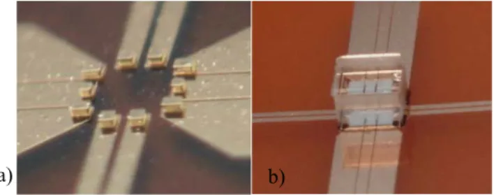
drawback: the gold stud bumping is a semi-manual process that lacks of reproducibility and reliability mainly when a large number of gold stud bumps/chip is required. The second method (with Au bumps developed on the Kapton surface) leads to a more reliable approach and is under development in our laboratory [4]. The Au bumps are created by using a technological process with the mains steps presented in Fig. 8. As shown in Fig. 9 a), we can assure a very good quality and alignment for the gold bumps directly fabricated/patterned on the Kapton. The Kapton structure represented in Fig. 9 a) was designed in order to accommodate a CMOS V-band low noise amplifier (LNA) designed in our laboratory and fabricated by using the 65 nm CMOS process from ST Microelectronics.
Fig. 9. a) Photo of the gold bumps patterned on the kapton surface; b) photo of the dummy chip mounted by a flip-chip process on the kapton surface
A lot of tests were performed by using dummy chip fabricated on glass substrate. The dummy chips have a size (400 µm x 400 µm) and a pad configuration identically with the ‘real’ LNA. A non-conductive adhesive polymer is deposited on the inner surface delimited by the Au bumps and the chip is stick by thermo-compression on the Kapton surface. The main challenge is how to deposit a non-conductive adhesive polymer on a surface as small as 240 µm × 250 µm on Kapton. Unfortunately up to now this method do not lead to 100% reliable process. During our multiple test, at least one contact (between the gold bump and the pads of the dummy chip) was negatively impacted by the presence of the non-conductive polymer. Works are underrun in order to find a more reliable procedure. An alternative method to overcome the adhesive issue can be the use of a raised-die under-fill configuration for the flip-chip [9].
IV. CONCLUSION
A kapton flexible technological process developed in our laboratory was presented. This process allow to obtain a very good resolution and quality for the metalization layers. Millimeter wave passive devices was manufactured by using this process. Very good performances were obtained for K-band cross dipole antenna array and V-K-band cross slot dipole antenna. Two technological process, under development in our laboratory for a flip-chip heterogenous integration technique that take into account the worst case constraints for millimeter wave applications, were also presented.
REFERENCES
[1] W. S. Wong and A. Salleo, Flexible Electronics: Materials and Applications. 2009.
[2] I. Toray Research Center, Printing Technology for Flexible Substrates. CA, USA: InterLingua Publishing, 2006.
[3] Dupont, “DuPont TM Kapton ®,” 2012. [Online]. Available:
http://www.dupont.com/content/dam/dupont/products-and- services/membranes-and-films/polyimde-films/documents/DEC-Kapton-general-specs.pdf.
[4] Z. Yang, “Flexible Substrate Technology for Millimeter Wave Applications”, Ph. D thesis of University of Toulouse, France, defended on Dec. 20, 2016.
[5] Z. Yang, A. Takacs, S. Charlot and D. Dragomirescu., "Flexible substrate technology for millimeter wave wireless power transmission", Wireless Power Transfer, Volume 3, Issue 1, March 2016, pp. 24-33. Cambridge University Press 2016.
[6] Z. Yang, A. Takacs, S. Charlot and D. Dragomirescu., "Design of Kapton based passive circuits at microwave frequencies," European Microwave Conference (EuMC), 2015, pp. 873-876.
[7] A. Takacs, H. Aubert, S. Fredon, L. Despoisse, H. Blondeaux, "Microwave power harvesting for satellite health monitoring, IEEE Trans. on Microwave Theory Tech, Vol.: 62, Issue: 4 , pp. 1090 - 1098, April 2014.
[8] M. M. Jatlaoui, D. Dragomirescu, S. Charlot, P. Pons, H. Aubert, and R. Plana, “3D Heterogeneous Integration of Wireless Communicating Nano-Sensors on Flexible Substrate,” SPIE Adv. Top. Optoelectron. Microelectron. Nanotechnologies, p. 78211E–78211E–7, 2010. [9] Z. Zhang, S. Luo, and C. P. Wong, “Recent Advances in Flip-Chip
Underfill: Materials Process and Reliability,” Adv. Flip Chip Packag., vol. 27, no. 3, pp. 155–199, 2013.