HAL Id: hal-01446107
https://hal.archives-ouvertes.fr/hal-01446107
Submitted on 25 Jan 2017
HAL is a multi-disciplinary open access
archive for the deposit and dissemination of
sci-entific research documents, whether they are
pub-lished or not. The documents may come from
teaching and research institutions in France or
abroad, or from public or private research centers.
L’archive ouverte pluridisciplinaire HAL, est
destinée au dépôt et à la diffusion de documents
scientifiques de niveau recherche, publiés ou non,
émanant des établissements d’enseignement et de
recherche français ou étrangers, des laboratoires
publics ou privés.
visible light on polyimide films
Philippe Molinié, Virginie Griseri
To cite this version:
Philippe Molinié, Virginie Griseri. Combined effects of charging, electron irradiation and visible
light on polyimide films. 14th Spacecraft Charging Technology Conference , ESA/ESTEC, Apr 2016,
Noordwijk, Netherlands. �hal-01446107�
COMBINED EFFECTS OF CHARGING, ELECTRON IRRADIATION AND VISIBLE
LIGHT ON POLYIMIDE FILMS
Philippe Molinié(1), Virginie Griseri(2)
(1) GEEPS (Group of electrical engineering), CentraleSupélec, Université Paris-Saclay,
3 rue Joliot-Curie, F-91192 Gif-sur-Yvette, France, [email protected]
(2)Université de Toulouse; UPS, INP; LAPLACE (Laboratoire Plasma et Conversion d’Energie);
118 route de Narbonne, F-31062 Toulouse, France. [email protected] ABSTRACT
Polyimide is widely used for spatial applications as it offers good thermal and electrical properties. In this paper an analysis of the photoconduction effect on charge transport in Kapton® HN films is proposed. Space charge distribution recorded by the Pulse Electro Acoustic Method and surface potential measurements may be explained by a simple model based on light absorption. Evidence is provided that, for strongly absorbed wavelengths, photoconductivity is leading to progressive charge injection, rather than charge vanishing under screening. A stable photoelectret may therefore be produced by light exposure on a charged sample. It may also be responsible for a strong return voltage effect on an apparently neutral film.
1. INTRODUCTION
The conduction properties of polyimide, especially Kapton®, under irradiation, have been largely studied in the context of spacecraft charging and are still under investigation [1-4]. Space charge measurements have been performed after electron irradiation in MEB [5-6]. Photoconduction is also well documented since pioneering works in the 1970s [7-9]. The maximum value of the photocurrent in the visible spectrum is reached for wavelengths corresponding to green light (between 500 and 580 nm) [9]. Detailed studies of photoconduction on several kinds of polyimides have shown that it is a two-step process, the absorption of a photon leading to an excited state of the PMDA-ODA molecule (charge transfer complex) which has to be ionized to give birth to a real conduction [9-11]. This is probably the main reason why this process is quite dependent on the applied field. The dark conductivity after the passage of a photocurrent is also known to be higher than its initial value.
However, there is no agreement on the conduction processes occurring in this material (for instance the charge carriers involved, holes [1,5], electrons [12], or ions [13], their mobility or the trap distribution density), maybe due to different experimental conditions. Furthermore, the variety of possible experimental environments and procedures is much larger than what has already been undertaken. For instance, the possible use of photoconduction in polyimide to produce a stable
charged film (photoelectret) has been underlined [14]. But we identified only one published work [8] devoted to the study of the effect of photoconduction on the space charge distribution inside of a polyimide film, and no reference to the possible consequences of the photoconduction heterogeneity due to light absorption. This work is investigating, through space charge and surface potential measurements, the combined effect of charging and exposure to visible light of different colors. It is shown that photoconduction at different wavelengths may be used to get a better knowledge on the internal space charge behavior on Kapton® films with simple laboratory experiments.
2. EXPERIMENTAL 2.1. Polyimide films
We used 125 µm Kapton® HN films without any metallization. In order to record the reference signal used to recover the space charge distribution by the Pulse Electro Acoustic (PEA) method a thin gold electrode is deposited by sputtering on one sample surface. This electrode is used to polarize the sample. The other films used under irradiation were not metalized nor submitted to any other treatment. Before corona charging and surface potential measurements, films were heated at 80°C during 1 hour and subjected to high intensity white light during 2 hours, to remove most of the internal charge.
The transmission and reflection spectra of the films were measured using a spectrophotometer at the GEEPS laboratory.
2.2. Electron irradiation and space charge measurements
Samples have been irradiated in the vacuum chamber called MATSPACE (Fig. 1) [15]. It is equipped with a thermionic gun that can provide electrons up to 100 keV with a flux of several nA/cm2. In the present paper we have irradiated the samples under 30 and 60 keV with a flux of 0.5 nA/cm2. The flux stability is controlled thanks to an electrometer display on which the current collected from a 1 cm2 electrode located on the sample holder in a Faraday cage arrangement is read. During
irradiation and relaxation samples are maintained under a vacuum environment of about 2.10-6 mbar.
To perform space charge distribution measurements in-situ the PEA method has been selected. Initially the method has been developed to study the behavior of dielectrics used for electrical engineering applications. Since several years, it has been modified so as to allow measurements under vacuum and after electron bombardment [16-19]. The sample is maintained on the detection electrode with a thin layer of cyanoacrylate glue. Measurements are performed between two periods of irradiation or lighting, and continuously during the relaxation.
Figure 1. Irradiation chamber MATSPACE equipped with a 100 keV electron gun. 2.3. Surface voltage measurements
Samples were charged in ambient air at 25°C using a classical corona triode (point-to-grid discharge, the insulator surface being charged at the grid potential). Charging time was 1 second and the deposited charge distribution circular. Surface voltage was then measured with an electrostatic voltmeter [20].
On each samples of a first series, the voltage decay after charging was recorded in the dark during 10 min for several initial grid positive and negative voltages. Then, the decay was recorded under blue LED or incandescent lamp illumination (depending on the samples), and immediately after, another voltage decay experiment was performed in the dark after a second application of the charge in order to check delayed photoconduction effects (Fig. 7 to Fig. 10).
A second series of samples were charged at +2 kV and exposed during various times to circular light dots coming from pipes canalizing the light emitted by a blue and a white LED. Their surface potentials were then neutralized by the use of a negative corona discharge using a grounded grid. Then the films were subjected to an incandescent lamp light with various exposition times. 2D voltage mapping of the initially charged area was performed after each of these steps (Fig. 11).
3. RESULTS 3.1. Light absorption
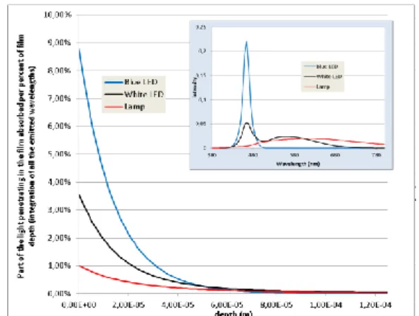
Figure 2. Transmission spectrum of the samples The measured ratio between incident and transmitted light is shown Fig. 2. The light reflection by the film (about uniformly 20%) has also been measured, accounting roughly for the observed difference between the measured transmission at the higher wavelengths and 100%. The transmission is decreasing very fast in the green/blue range. Assuming a homogeneous absorption in the film, monochromatic light intensity follows an exponential decay within the bulk with a characteristic penetration length of about 63 µm at 530 nm (green) and about 13 µm at 465 nm (blue). From the spectra of the three light sources used (incandescence lamp, blue and white LED), measured in laboratory for the lamp, and coming from literature for the LED, we computed the total relative light absorption in the volume for these three sources, the insulator being divided in 100 slices, by integration of the exponential absorption curves for all the significant wavelengths of the spectrum. We considered only wavelengths below 550 nm to be able to produce ionization (this threshold is somewhat arbitrary, but may be adjusted later). The result, shown Fig. 3, will be used in the model. Reflection on the back electrode is not taken into account.
Figure 3. Light absorption profiles for three different light sources (λ<550 nm)
3.2. Space charge measurements after electron irradiation and light exposure
A first irradiation using 30 keV electron beam leads to a negative peak with a maximum at about 6 µm below the irradiated surface (fig. 4).
Figure 4. Charge density after 30 keV irradiation
Open-PEA system, 30 keV irradiation on 125 µm Kapton® HN film during 45 s and additional 40 s, under a flux of 0.5 nA/cm2.
Charges are detected up to 13 µm below the surface. The peak does not return to zero at the sample surface because there is a reflection of the signal at the interface sample/vacuum which acts as a mirror. That is why a negative image signal, which will not be taken into account, appears in the region located beyond 125 µm. Positives induced charges are detected on the back electrode. The amplitudes of both peaks increase with the irradiation time.
A subsequent irradiation with higher energy (60 keV) electrons creates a peak with a maximum at a depth of 23 µm (end of peak 30 µm below the surface) (fig. 5). Another feature appears clearly: the 30 keV peak at 6 µm has vanished, while a negative surface peak has appeared. In these first two experiments, the amount of positive charge on the back electrode seems also to be roughly proportional to the charging time.
Figure 5. Effect of an additional 60 keV irradiation
Open-PEA system, additional 60 keV irradiation on 30 keV charged (Fig.3) 125 µm Kapton® HN film during 30 s, under a flux of
0.5 nA/cm2, and 19 min relaxation.
Then, the sample is illuminated with an incandescent lamp during 3 minutes. The result is the screening of the negative 60 keV charge peak, while part of the negative charge seems to accumulate near the back electrode. The amount of positive charge on this back electrode is also reduced.
Figure 6. Effect of an additional illumination
Open-PEA system, additional 3min illumination with an incandescent lamp, on a 30 keV+60 keV charged (Fig. 5) 125 µm Kapton® HN
film, and 13 min relaxation.
3.3. Surface voltage measurements
The raw data of surface potential decay in the dark and under illumination using a white incandescent lamp is shown as an example Fig. 7 for various initial corona charging levels. A significant feature is the strong dependence of the photoinduced decay on the applied field, with a “crossover” point observed above 2000 V in negative polarity.
Figure 7. Surface potential decay after corona charging
1 s corona charging with triode at several initial grid potentials, on 125 µm Kapton® HN films, in the dark (dotted lines) or under
incandescent lamp illumination (solid lines).
0 20 40 60 80 100 120 -300 -200 -100 0 100 200 300 400 Injected charges 125 µm C ha rg e de nsi ty (C /m 3) Distance (µm) 30 keV Irradiation 45 s Irradiation 85 s Irradiation direction Induced charges 0 20 40 60 80 100 120 -300 -200 -100 0 100 200 300 400 125 µm C ha rg e de nsi ty (C /m 3) Distance (µm) 60 keV Irradiation 30 s Relaxation 5 min Relaxation 9 min Relaxation 14 min Relaxation 19 min Irradiation direction Injected charges 0 20 40 60 80 100 120 -300 -200 -100 0 100 200 300 400
60 keV Relaxation 19 min Light 3 min Relaxation 1 min Relaxaxation 4 min Relaxation 13 min C ha rg e de nsi ty (C /m 3) Distance (µm) Irradiation direction -3500 -2500 -1500 -500 500 1500 2500 3500 0 100 200 300 400 500 600 Su rface p o te n tial ( V) time (s)
Figure 8. Voltage decay rates, under white light
Incandescent lamp illumination. Voltage rates reduced to the value of the initial voltage.
Figure 9. Voltage decay rates, under blue light
Blue LED illumination. Voltage rates reduced to the value of the initial voltage.
The time derivative of the potential has been computed for these data, for the decay under blue LED exposure, and for the second dark decay measured immediately after the measurements under illumination. It is
represented in a log-log plot in Fig. 8 and Fig. 9, normalized to the charging surface potential V0.
Figure 10. Voltage decay rates, in the dark before and after illumination
10 min blue LED illumination at the same initial voltage. Voltage rates reduced to the value of the initial voltage.
The field dependence of the represented values is clear on these plots, together with a first order independence on the applied polarity. Comparing the results between white and blue exposures, it is also noticeable that the first data set exhibits a constant voltage decay rate in the first ten seconds, while the decay rate under blue light exposure decreases from the first seconds.
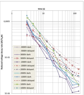
The comparison of the decay rates in the dark before and after blue light illumination is shown Fig. 10. A significant difference is visible at long decay times, especially for the highest voltages. The same is observed using white light.
The build-up of an internal space charge through the effect of light has been clearly shown by return voltage measurements. A typical result is displayed on the potential mappings Fig. 11. In (a), a 2 kV charged surface has been subjected to the light of a white (left) and a blue (right) LED. The potential of the central zone of the surface has then been reduced to a low (slightly negative) value using a negative discharge of the opposite polarity, with a grounded grid. No apparent trace of the applied light beams is left (b). However, exposing the film to a uniform intense white light from an incandescence lamp progressively reveals the
5E-05 0,0005 0,005 1 10 100 R e d u ce d v o ltage d e cay r ate (d V/ V0 d t) time (s)
Incandescence bulb light
-3000V 3000V -2000V 2000V -1000V 1000V -500V 500V 5E-05 0,0005 0,005 1 10 100 R ed u ce d v o ltage d ec ay r ate (d V/ V0 d t) time(s)
Blue LED light
-3000V 3000V -2000V 2000V -1000V 1000V -500V 500V 5E-06 5E-05 0,0005 1 10 100 R e d u ce d v o ltage d e cay r ate (d V/ V0 d t) time (s) -3000V dark -3000V delayed 3000V dark 3000V delayed -2000V dark -2000V delayed 2000V delayed 2000V dark -1000V dark -1000V delayed 1000V dark 1000V delayed
internal charging heterogeneity of the film as may be shown by (c) to (h).
(a) (b)
(c) (d) (e)
(f) (g) (h)
Figure 11. Voltage mappings showing light-induced decay and return voltages.
Exposure 120 s to white (left) and blue (right) LED light after +2 kV charging (a). Quasi neutralization (b) Return voltages under lamp illumination, with total duration 30 s (c), 150 s (d), 750 s (e), 3600 s
(f), 7200 s (g), 10000 s (h)
4. A SIMPLE NUMERICAL MODEL
A simple 1D model of the problem may be built, by considering an insulating material with a permittivity 𝜀 and thickness L. The boundary conditions are a null field above the material (corresponding to the electrostatic voltmeter probe) and a null voltage in the metal plate below the film.
Charge density x qm x 0 L E=0 for x<0 V(t) + + + + + + + + + + + + - - - - Photoconductivity light x + - - + - + + - Field E x
Figure 12. Voltage decay under illumination A uniform charge density q0 has been deposited at t=0 on the surface (which may be simulated by a quickly
decreasing exponential charge distribution ρ(x,0)), and the insulator is exposed to a light source with a complex spectrum from above. The photoconduction is induced by the light partial absorption by the insulator, generating an amount of electron-hole pairs proportional to this absorption. The conductivity is therefore a function of the ratio of the depth below the surface. We computed for each light source the efficient light absorption dΦ/dx as mentioned above and we assume that: 𝜎(𝑥) = 𝜎0 𝑑𝜙 𝑑𝑥 (𝑑𝜙𝑑𝑥) 𝑥=0 (1)
Assuming that the space charge is steadily trapped at the timescale of the experiment, the current density is only due to the induced photoconductivity:
𝑗 = 𝜎(𝑥)𝐸 (2)
This current will then be able to screen the trapped charge (for instance electrons neutralizing the positive surface charge density), therefore leading to a displacement of the charge distribution. This may however be done with or without recombination. The initial charge may therefore still be present in deep levels. Introducing the charge conservation 𝑑𝑗
𝑑𝑥+ 𝑑𝜌 𝑑𝑡 = 0 we obtain: 𝑑𝜌 𝑑𝑡= − 𝑑𝑗 𝑑𝑥= − 𝑑 𝑑𝑥[𝜎(𝑥)𝐸(𝑥)] (3)
The field E may be computed using the upper boundary condition E=0 through Poisson equation 𝑑𝐸
𝑑𝑥=
𝜌
𝜀.
From this a calculation of the space charge evolution with time has been done. The result is shown on Fig. 13. To calibrate each simulation, we ensured that the potential decay observed in 600 s was the same than what was observed in the experiments. The overall light intensity of the different sources may be different.
At short times, the field is still almost uniform in the volume of the insulator, and the charge density build-up in any point of the insulator by the light exposure
𝑑𝜌
𝑑𝑡 = −
𝑑𝑗
𝑑𝑥≈ −𝐸
𝑑𝜎
𝑑𝑥 is roughly proportional to the
photoconductivity gradient. For longer times, space charge motion will be slowed by the lower conductivity layers, and a quasi-steady state will appear in the form of a space charge peak, whose width depends on the light absorption length, which will drift more and more slowly into the bulk. This is clearly visible in the simulation results (fig. 13) concerning the blue LED. For the white LED, part of the charge is evacuated through the rear electrode, and the charge distribution is progressively reduced.
Figure 13. Computed space charge profiles Cutting off the illumination will freeze charge motion. Surface neutralization may then be assumed as the deposit of a given amount of negative surface charge to bring back the surface voltage to zero. This creates a field inversion in the upper part of the insulator (Fig.14).
This charge distribution is assumed to be steadily trapped, but another illumination of the surface will induce a larger conductivity in this inverse field zone than in the lower part of the sample, due to light absorption. As a result, a return voltage appears, due to the progressive compensation of the negative surface charge by a fraction of the internal positive charge.
x qm x 0 L E=0 for x<0 V(t) + + + + + + + + - - - - Photoconductivity light x + - - + - + - + - qs - - - - - - Field E x Charge density
Figure 14. Return voltage under illumination
This is illustrated by Fig. 15 for white and blue LED spectra. The fact that the photoconduction induced during this second illumination is assumed to be done with the same lamp in both cases is taken into account.
Figure 15. Computation of the return voltage under illumination
Return voltages under lamp illumination, after blue and white LED photo-activated decay for a given duration (500s)
5. DISCUSSION
5.1. Space charge measurements
The PEA data for the successive 30 keV and 60 keV irradiations described here show that most of the electron charge has not been evacuated from the sample. However, Fig. 5 also shows that part of the electronic charge has progressed towards the back electrode. That may imply that, during charging, the deposited electrons mobility cannot be neglected at this high value of the fields (the maximum computed value for this figure is close to 200 kV.mm-1, and the surface potential exceeds -25 kV). However, after charging, this charge distribution seems to be quite steady.
The effect of radiation-induced conductivity in the upper part of the film appears clearly with the fading of the 30 keV peak. Charge conservation implies that part of this peak charge peak drifted inside the film to join the 60 keV peak, while another part returned to the surface. This may be attributed to the electrostatic environment of the insulator, with the presence of a ground electrode not very far from the upper surface (2 mm), producing a field inversion in the upper part of the insulator.
The influence of light on the charge distribution displayed Fig. 6 maybe easily understood using the decreasing conductivity model developed above. Photoconduction has efficiently reduced the amount of
0 2 4 6 8 10 12 14
0,00E+00 2,00E-05 4,00E-05 6,00E-05 8,00E-05 1,00E-04 1,20E-04
S p ac e c h ar g e d e n si ty (ar b . u n it.) depth (m) White LED t=1000s t=500s t=200s t=0s 0 2 4 6 8 10 12 14
0,00E+00 2,00E-05 4,00E-05 6,00E-05 8,00E-05 1,00E-04 1,20E-04
S p ac e c h ar g e d e n si ty (ar b . u n it.) depth (m) Blue LED t=1000s t=500s t=200s t=0s 0 20 40 60 80 100 120 140 160 0 200 400 600 800 1000 R e tu rn v o ltage (V) time (s)
White LED (neutral. 500s) Blue LED (neutral. 500s)
space charge present in the top half of the sample but the residual charge tends to increase with the depth. This charge seems also to remain steady after the end of illumination.
5.2. Surface voltage
The voltage decay under illumination exhibits a quite good symmetry between positive and negative polarities. This is a sign of a process which does not rely on a particular carrier mobility, but rather on a bipolar process, in this case photoconduction by electron-hole pair creation. This may be different at higher fields, where the generated electrons (or holes) may have a larger mean free path (as has been assumed above in the 60 keV MATSPACE experiment).
At short times, a constant decay rate regime appears for white light, which cannot be found using blue light. The decay has a constant rate as long as most of the charge distribution is surrounded by a volume with conductivity close to its surface value. The characteristic duration of this regime is depending on the light penetration length. Conduction is higher near the surface using blue light, which is more absorbed, but decreases much quicker, for the same reason.
There is a strong field effect on photoconductivity, which is clearly visible at short times. This effect is balanced at long decay times by the fact that the charge distribution has progressed deeper into darker zones of the film when the voltage was initially higher.
In this voltage range, the dark decay is quite independent from the polarity and the initial voltage. However a delayed photoconductivity appears which cannot be neglected for the longer time values and the higher values of the applied voltage. This phenomenon seems to be linked to the photoconduction intensity in the previous stage.
The return voltage observed for neutralized films under illumination confirms the internal build-up of a space charge under the influence of a previous illumination.
The shape of the return voltage with time behaves qualitatively as the model predicts, with a faster return and also an earlier maximum for blue light, than for white light.
5.3. Evaluation of the numerical model
Our numerical model has been used only to provide a visual explanation of the main features underlying the influence of photoconduction on the space charge. It has to be improved to lead to precise values that may be useful for the engineer.
Let us underline the limits of our model: first, the photoconductivity dependence on the field has been neglected. Second, the space charge is assumed to be deeply trapped, and its own mobility is neglected. However, it is interesting to remark that our model provides a good explanation for the observed surface potential measurements:
a) Heterogeneous photoconduction does not lead to a progressive vanishing of the space charge distribution (as would be the result of a homogeneous conductivity) but rather to a progressive drift into the bulk, depending on the wavelength. As a result, the voltage decay rate, even neglecting the photoconduction dependence on the field, decreases quickly with time, especially for the most absorbed wavelengths.
b) The main differences in the return voltage kinetics measured under illumination at different wavelength may be understood in a simple way using this model. The highest initial rate of the voltage return using blue light has to be attributed to a shorter mean space charge depth.
6. CONCLUSIONS
The work undertaken by our teams rely on classical experiments, on a classical material. But it is worth to underline that the existence of space charge effects due to the gradient of light absorption presented here have been neglected until now. They seem to us worth publishing, from several points of view.
First, the hypothesis of fast and steady retrapping of the charge at low fields is confirmed by our results. A macroscopic injection of the charge distribution may occur without any detrapping of the charge itself, as a mere result of heterogeneous screening by photoinduced carriers (having a short free mean path at low fields), assuming a photoconductivity gradient. Recombination of the initially deposited charge with the photoinduced carriers of the opposite polarity may, or may not occur, our model cannot answer to this question.
From a practical point of view, it has been shown that with a very simple device (for instance a corona charge, and an incandescent lamp) it is possible to produce a stable photoelectret on Kapton®, with a positive or negative charge distribution at various depths. Kapton® has already been used in the past to produce such a stable photoelectret [8,14], but it seems that this has never been analyzed as a consequence of the light absorption gradient. Using different wavelengths and
illumination times, it is also possible to change the charge distribution in the film.
This tunable photoelectret may have practical implications. It may be used to get information on the internal charge stability of electron and holes, by using thermal techniques and promoting charge migration at high fields. The use of different wavelengths after surface neutralization may also be implemented with surface voltage measurements to get a 3D picture of the inner charge distribution.
Concerning the electrostatic risk pertinent for the spacecraft charging community, it is also worth to underline that this stable photoelectret effect is part of the strong memory effects experienced in disordered insulators: a surface neutralization of the insulating films cannot guarantee a neutral volume. Quite large and stable charge densities may be present in the films, which may induce important surface voltages, when subjected to a simple illumination, without any external charging source.
ACKNOWLEDGMENT
P.M wishes to thank Alexandre Jaffré from GEEPS laboratory for performing spectrophotometry measurements.
7. REFERENCES
1. Tyutnev, A.P., Ikhsanov, R.S., Marchenkov, K.V., Saenko, V.S., Pozhidaev, E.D., 2008, Dose effects in radiation-induced conductivity of polypyromellitimide, Polymer Sc. Series A, 50, 429–433.
2. Molinié, P., Dessante, P., Hanna, R., Paulmier, T., Dirassen, B., Belhaj, M., Payan, D., Balcon, N., 2012. Polyimide and FEP charging behavior under multienergetic electron-beam irradiation, IEEE Trans. Diel. E.I., 19, 1215–1220.
3. Paulmier, T., Sicard-Piet, A., Lazaro, D., Arnaout, M., Payan, D., 2015. Analysis of Charging Kinetics on Space Dielectrics Under Representative Worst Case Geostationary Conditions, IEEE Trans. Plasma Sc., 43, 2849– 2855.
4. Tyutnev, A., Saenko, V., Pozhidaev, E., Ikhsanov, R., 2015. Experimental and Theoretical Studies of Radiation-Induced Conductivity in Spacecraft Polymers, IEEE Trans. Plasma Sc., 43, 2915 – 2924.
5. Sessler, G.M., Hahn, B., Yoon, D.Y., 1986. Electrical conduction in polyimide films, J App. Phys., 60, 318.
6. Sessler, G.M., Yang, G.M., 1999. Charge dynamics in electron-irradiated polymers, Brazilian J. Phys. 29.
7. Coffey, H.T., Nanevicz, J.E., Adamo, R.C., 1975. Photoconductivity of high voltage space insulating materials (Tech. Report No. NASA-CR-134995). 8. Cals, M.-P., Marque, J.-P., Alquié, C., 1992.
Direct observation of space charge evolution in e-irradiated Kapton films, IEEE Trans. E.I., 27, 763–767.
9. Hasegawa, M., Horie, K., 2001. Photophysics, photochemistry, and optical properties of polyimides, Progress in Polymer Sc., 26, 259–335. 10. Kowalczyk, S.P., Stafström, S., Brédas, J.L., Salaneck, W.R., Jordan-Sweet, J.L., 1990. Electronic structure of polyimide and related monomers: Theory and experiment, Phys. Rev. B 41, 1645.
11. LaFemina, J.P., Kafafi, S.A., 1992. Electronic structure and photophysical properties of polyimides. Pacific NW Lab., Richland, WA-US. 12. Tu, N.R., Kao, K.C., 1999. High-field electrical
conduction in polyimide films, J. App. Phys., 85, 7267–7275.
13. Raju, G.G., Shaikh, R., Haq, S.U., 2008. Electrical conduction processes in polyimide films - I., IEEE, Trans. Diel. E.I., 15, 663–670.
14. Quamara, J.K., Pillai, P.K.C., Sharma, B.L., 1982. The photoelectret state in kapton polyimide film. I. The effect of polarizing temperature, field and time, Acta Polymerica, 33, 501–503.
15. Griseri, V., Malava, P., Berquez, L., Tung, T.A., Le Roy, S., Boudou, L., Boulanger, A., 2010, Charge Build-Up and Transport in Electron Beam Irradiated Polymers in a New Irradiation Chamber, Annual Report CEIDP, IEEE conference.
16. Griseri, V., Laurent, C., Fukunaga, K., Maeno, T., Lévy, L., Payan, D., 2004, The Pulsed Electro-Acoustic Technique Applied to In-Situ Measurement of Charge Distribution in Electron-Irradiated Polymers, IEEE Trans. Diel. E.I., Vol. 11, 5, 891-898.
17. Perrin, C., Griseri, V., Laurent, C., 2008, Measurement of Internal Charge Distribution in Dielectrics Using the Pulsed Electro-Acoustic Method in Non-Contact Mode, IEEE Trans. Diel. E.I., Vol. 8, 4, 958-964.
18. Griseri, V., Nguyen, X.T., Berquez, L., 2013 Analysis of the Pulsed Electro-Acoustic Signal Treatment Recorded on Electron Beam Irradiated Dielectrics, J. Electrostatics, Vol. 71, 3, 422-428 19. Dispositif pour déterminer une répartition de
charges dans un élément diélectrique, Patent, FR2917836A1, 2007.
20. Molinié, P., 2005, Measuring and Modeling Transient Insulator Response to Charging: the Contribution of Surface Potential Studies, IEEE Trans. Diel. E.I., 12, 939-950