Continuous Wave Operation of
a Mid-Infrared Semiconductor
Laser at Room Temperature
Mattias Beck,
1* Daniel Hofstetter,
1Thierry Aellen,
1Je´roˆme Faist,
1Ursula Oesterle,
2Marc Ilegems,
2Emilio Gini,
3Hans Melchior
3Continuous wave operation of quantum cascade lasers is reported up to a temperature of 312 kelvin. The devices were fabricated as buried heterostructure lasers with high-reflection coatings on both laser facets, resulting in continuous wave operation with optical output power ranging from 17 milliwatts at 292 kelvin to 3 milliwatts at 312 kelvin, at an emission wavelength of 9.1 microme-ters. The results demonstrate the potential of quantum cascade lasers as con-tinuous wave mid-infrared light sources for high-resolution spectroscopy, chem-ical sensing applications, and free-space optchem-ical communication systems. The mid-infrared portion of the spectrum,
covering approximately the wavelength range from 3 to 12m, is sometimes referred to as “underdeveloped” because of its lack of
con-venient coherent optical sources. Especially when compared to the visible or near-infrared spectral range, where interband semiconduc-tor lasers are now produced very economical-ly with continuous wave (CW) output power of tens of milliwatts, this assertion holds true. In the mid-infrared, a new class of semicon-ductor lasers—intersubband quantum cas-cade (QC) lasers (1)— has become a promis-ing alternative to interband diode lasers (2, 3) in the past 7 years. In these devices, photon emission is obtained by electrons making op-tical transitions between confined energy lev-1Institute of Physics, University of Neuchaˆtel,
CH-2000 Neuchaˆtel, Switzerland.2Institute of Micro- and
Optoelectronics, Department of Physics, Swiss Feder-al Institute of Technology, CH-1015 Lausanne, Swit-zerland.3Institute for Quantum Electronics,
Depart-ment of Physics, Swiss Federal Institute of Technolo-gy, CH-8093 Zurich, Switzerland.
*To whom correspondence should be addressed. E-mail: [email protected]
Published in Science 295, no 5553, 301-305, 2002 which should be used for any reference to this work
els. As such, QC lasers can be fabricated from wide-bandgap technologically mature semiconductors, and their emission wave-length can be tailored over a wide range by changing only the layer thicknesses. In addi-tion, because their main nonradiative mecha-nism is optical phonon emission and because of the atomic-like joint density of states of intersubband transitions, QC lasers exhibit a gain that is weakly temperature dependent. As a result, QC lasers have demonstrated high mid-infrared output powers in pulsed operation up to temperatures above 400 K (4 ). However, CW operation of QC lasers based on standard designs has remained lim-ited to cryogenic temperatures below 175 K (5). A recent active region design enabled CW operation up to 243 K (6 ), which is barely high enough to be maintained by a thermoelectric cooler.
Because the main nonradiative mecha-nism in mid-infrared interband lasers is Au-ger recombination, these devices exhibit a much stronger temperature dependence of the threshold current density, and CW operation is limited to temperatures below 225 K (2).
Although chemical sensing based on
op-tical absorption has been successfully dem-onstrated with pulsed QC lasers (7 ), these systems are typically limited by the fairly wide emission linewidth of the QC laser (⬎500 MHz); high sensitivity can only be achieved with the narrow linewidth of a CW-operated device (8). Mid-infrared at-mospheric optical communication systems (9, 10), using QC lasers for data transmis-sion through the two transparent atmo-spheric windows, will potentially benefit from light sources operating in CW mode at noncryogenic temperatures.
The limiting factor for CW operation of semiconductor lasers is the large heat dissi-pation. At high duty cycles, the temperature of the active region Tactis much higher than
the heat sink temperature Tsink. In a simple model (11), the heat transport between active region and heat sink is characterized by the thermal conductance Gthper unit of area of the active region; that is, Tact⫽ Tsink⫹ U ⫻
Jth/Gth at threshold. Assuming a constant
threshold voltage U and that the temperature dependence of the threshold current density
Jthcan be described by the phenomenological relation Jth⫽ J0exp(Tact/T0), the maximum
CW operating temperature Tsink,maxof a QC laser is given by Tsink,max⫽ T0⫻ [ln(T0Gth/
J0U) – 1]. A high value of the characteristic
temperature T0is therefore an absolute
neces-sity to achieve room-temperature CW opera-tion. The large value of T0achieved in recent QC laser structures (T0⬎ 170 K) results in a
low temperature sensitivity of Jthand shows
the potential of these devices for CW opera-tion. However, the devices used in the early attempts to reach high-temperature CW op-eration (12, 5) had a J0U product of about 10
kW/cm2. This value, corresponding to a
threshold current density of ⬃5 kA/cm2 at
300 K, is just too large to be evacuated from the active region when the laser is operated at high duty cycles, even assuming an idealized device geometry.
In addition, the actual core temperature is equal to Tact⫽ T0⫻ ln(T0Gth/J0U) when the
laser is operated at Tsink,max(13), resulting in a temperature difference between the active region and the heat sink of T0. For large T0
values, the device might fail by thermal stress before reaching the temperature Tsink,max. For this reason, it is essential to (i) minimize the threshold current density and (ii) use a device geometry that minimizes thermal stress. To reduce the room-temperature threshold cur-rent density, active region designs based on a double-phonon resonance (6 ) and a bound-to-continuum transition (14 ) were recently developed. In these structures, the injection and extraction efficiency to and from the active region were significantly improved by means of wave function engineering. Addi-tionally, growth conditions and the doping concentration of the active region were opti-mized. As a consequence, the pulsed thresh-old current density at 300 K dropped to a value as low as 3 kA/cm2(6 ).
We present QC lasers with an active re-gion based on a double-phonon resonance and designed for a lasing transition at an energy of 135 meV (corresponding to a wavelength of 9.18 m) between the upper and lower lasing states (levels 4 and 3 in Fig. 1A). The active region is composed of four quantum wells (QWs), which results in three coupled lower energy states (levels 1, 2, and 3) separated from each other by one phonon energy (15). The active region used a narrow QW-barrier pair just after the injection barrier [similar to the classical three-QW design (16 )] that enhances the injection efficiency into the upper lasing level by increasing lo-cally the magnitude of the upper state wave function (12). The observation of a clear res-onant tunneling effect in structures with a three-QW active region demonstrated the ef-fectiveness of this approach (17 ).
The fast intersubband scattering between the lowest subbands separated by an optical phonon energy should lead to a high popula-tion inversion in a three-QW active region
Fig. 1. (A) Schematic
conduction-band dia-gram of one period of the laser core with moduli-squared rele-vant wave functions in the four-QW active region based on a dou-ble-phonon resonance. The red wavy arrow in-dicates the transition responsible for laser action, and green ar-rows represent optical phonon transitions. (B) Computed temperature contours around the ac-tive lasing region of the buried heterostructure QC laser at room tem-perature. The solid lines display the geometry of the different materials used in the simulation, and the dashed lines represent the geometry of the laser. (C) Com-puted thermally in-duced stress in the ac-tive region. The maxi-mum stress occurs at the corner of the active region.
device, even at room temperature. However, the relatively slow measured tunneling time from the active region of about 2 ps (18, 19) intro-duces an effective bottleneck to the electron transport, enhancing the lower laser state pop-ulation. A model of the room-temperature elec-tron kinetics in the active region (20), which included optical phonon emission and absorp-tion from all points in k-space of the active region subbands, demonstrated that this bottle-neck effect resulted in an effective lower state lifetime as long as 0.8 ps for a typical three-QW structure. The same computation also shows that the presence of an additional state in the active region (that is, level 1) allowing the emission of two optical phonons from the lower laser level decreases the lifetime of that level down to 0.5 ps. As a result, the computed ratio between the upper and lower state population increased from 1.9 for the three-QW structure to 2.8 in the double-phonon resonance struc-ture, simultaneously decreasing the threshold current density and increasing the slope effi-ciency and maximum power, as was indeed observed (6).
Moreover, our devices were processed in a narrow-stripe, planarized, buried hetero-structure geometry (21), in which the gain region was vertically and laterally buried within InP cladding layers, the geometry of which provides a number of advantages. The choice of a buried stripe greatly improves the heat transport by allowing heat flow from all sides of the active region. Additionally, the narrow-stripe geometry also decreases the to-tal amount of strain that builds up in a mate-rial subjected to a very strong temperature gradient. Indeed, the results from a simula-tion, done with a commercial finite-elements differential equation solver (22), of both ther-mal transport and therther-mally induced stress lead to the same conclusions (Fig. 1, B and C). A thermal conductance of 820 W/Kcm2is
predicted for a buried, 12-m-wide, junction-down–mounted device, as compared to the calculated value of 510 W/Kcm2 for a
28-m-wide, ridge, junction-down–mounted de-vice (6 ). Similarly, the maximum thermally induced shear stress that builds up at the edges of the active region (Fig. 1C) decreases from 22 MPa in the ridge device to 3.6 MPa for the buried structure.
Fabrication of the laser structure relied on molecular beam epitaxy for the growth of the lattice-matched InGaAs/InAlAs laser core on an InP substrate. The laser core consists of 35 periods, each comprising a partially n-doped injector region and the undoped four-QW active region, embedded in an optical waveguide formed on one side by the sub-strate and a lower InGaAs waveguide layer and on the other side by an upper InGaAs waveguide layer and the InP top cladding, which was grown by metalorganic vapor-phase epitaxy (MOVPE).
The lasers were fabricated into 12- m-wide buried stripes by wet etching and selec-tive MOVPE regrowth of i-InP using a SiO2
mask. The devices were then cleaved into 750-m-long lasers, soldered junction-down onto a diamond platelet, and finally facet-coated by a ZnSe/PbTe high-reflectivity (R⫽ 0.7) layer pair.
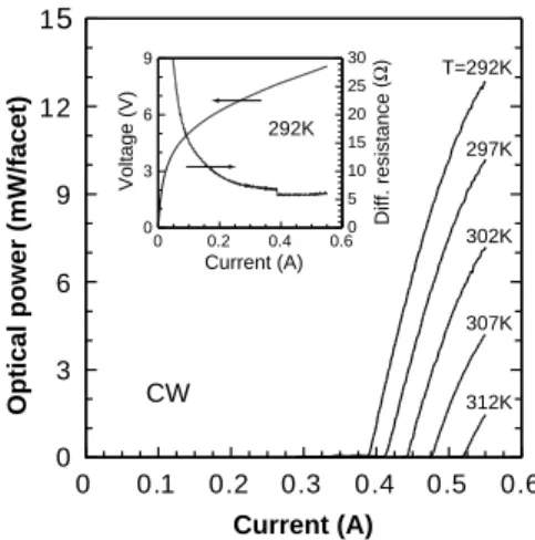
The CW optical output power emitted from one facet (Fig. 2) was measured with a calibrated thermopile detector, which was mounted directly in front of the laser facet. At room temperature (292 K), the laser exhibited a threshold current of 390 mA (corresponding to a threshold current density Jth⫽ 4.3 kA/
cm2
at a voltage bias U⫽ 7.6 V) and a slope efficiency dP/dI of 101 mW/A (where P is optical power and I is current). This device emitted 13 mW of optical power from a single facet at a driving current of 550 mA, resulting in a wall plug efficiency of 0.55% per facet. Continuous wave operation was observed up to 312 K (39°C). At this temper-ature, the threshold current increased to 520 mA ( Jth⫽ 5.8 kA/cm2), while still more than
1 mW of output power was emitted at 550 mA. The electrical transport characteristics of the device (inset of Fig. 2) display the expect-ed discontinuity of the differential resistance at threshold (390 mA).
A laser with the same cavity length but a slightly larger stripe width of 15m emitted 17 mW per facet at a drive current of 600 mA at room temperature. This device could be operated up to 311 K, with a maximum op-tical power of 3 mW and a threshold current of 540 mA ( Jth⫽ 4.8 kA/cm2).
The performance of these buried hetero-structure devices demonstrates the results of the thermoelastic predictions. Although the junction-down–mounted, 28-m-wide, con-ventional ridge lasers failed systematically at 4 kA/cm2(6 ), the 12-m-wide buried lasers
discussed in this paper supported more than 6 kA/cm2.
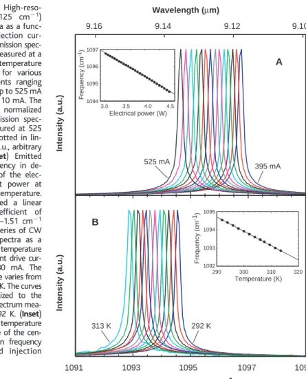
The emission frequency of a QC laser can be tuned over a small range of a few cm⫺1by changing the current and tempera-ture. The CW spectral properties were ana-lyzed with a Fourier transform infrared spec-trometer. The emission spectra (Fig. 3A) col-lected at a constant heat sink temperature of 292 K and various currents between 395 and 530 mA reveal frequency tuning from 1096.74 cm⫺1to 1094.54 cm⫺1, linear with the electrical input power (inset of Fig. 3A). At a fixed current of 530 mA, the emission frequency of the laser shifts from 1094.54 cm⫺1at 292 K to 1092.90 cm⫺1 at 313 K (Fig. 3B). The measured center frequencies are well fitted by a linear function (inset of Fig. 3B) with a tuning coefficient of⌬/⌬T ⫽ – 0.078 cm⫺1/K. Single mode emission was observed for this particular device over the whole investigated current and temperature
range, with a side mode suppression ratio better than 30 dB. This rather surprising fact can be explained by a small defect within the laser cavity, as indicated by an intensity mod-ulation of the subthreshold Fabry-Perot fring-es at twice the cavity mode spacing.
Assuming that the emission frequency is a function only of the temperature of the active region, we can deduce a thermal resistance Rth of the device from the vari-ation of the emission frequency (11) with
Rth ⫽
冉
⌬T ⌬P冊
⫽冉
⌬ ⌬P冊
⫻冉
⌬ ⌬T冊
⫺1 . Inserting the above tuning rates, we get a thermal resistance of 19.4 K/W in the range between 292 K and 313 K (corresponding to a thermal conductance Gth of 574 W/Kcm2).This Rthvalue is higher than the calculated one (13.6 K/W), most likely because the thermal interface resistance was not included in our simulation.
The dependence of the threshold current density Jthon the actual core temperature Tact
of the laser is measured in pulsed mode at low duty cycles, where heating effects are negligible (that is, Tact⬃ Tsink). At 292 K, we measured a pulsed Jthas low as 3.1 kA/cm
2
(compared to 4.3 kA/cm2
in CW operation) for the 12-m-wide device, corresponding to a threshold current Ith⫽ 280 mA. The exper-imental pulsed threshold current densities (Fig. 4) can be fitted by the expression Jth⫽ J0exp(Tact/T0) with a T0⫽ 171 K and J0⫽ 560 A/cm2.
The temperature dependence of the CW threshold current density can be computed from the data in pulsed operation, using a slightly modified model that takes into ac-count the change in applied voltage with
Current (A)
Optical power (mW/facet)
0 0.1 0.2 0.3 0.4 0.5 0.6 0 3 6 9 12 15 CW T=292K 302K 312K 297K 307K Current (A) Diff. resistance 292K 0 5 10 15 20 25 30 0 0.2 0.4 0.6 0 3 6 9 Voltage (V)
Fig. 2. CW optical power from a single laser
facet as a function of drive current for various heat sink temperatures. The laser is 0.75 mm long and 12m wide. The power was measured with near-unity collection efficiency and a cal-ibrated thermopile detector. (Inset) Electrical transport characteristics of the laser at 292 K: bias voltage as a function of injection current and differential resistance deduced from the V-I curve.
injected current (23) and uses the thermal conductance Gthobtained from the spectral measurements. The calculated Jthcurve fits well with the experimental CW Jth values
(solid symbols in Fig. 4). The data also show that, at 292 K, the temperature differ-ence⌬T ⫽ Tact– Tsink between laser core and heat sink is 58 K at threshold and increases to 87 K at the maximum injected current. With this modified model, we
cal-culate a maximum CW operating tempera-ture Tsink,max⫽ 321 K and a ⌬T ⫽ 119 K at that operating temperature.
The threshold currents of our buried het-erostructure QC lasers scale accurately with the laser stripe width (inset of Fig. 4). It means that our device architecture does not introduce additional lateral waveguide losses or current leakage paths.
The far-field distributions in the two
direc-tions parallel and perpendicular to the grown layers exhibited a Gaussian profile with far-field angle of 40° full width at half maximum in the in-plane direction and 80° perpendicular to the layers, proving that the device oscillates in its fundamental lateral and transverse mode.
Fundamental intersubband processes did not limit the device performance. Assuming the measured waveguide loss value of 10 cm⫺1 (24) and in the limiting case of unity injection efficiency, the threshold current density of our QC laser should be 2.1 kA/cm2
(25), which is significantly lower than the measured value (3.1 kA/cm2). We believe that further
improve-ments in active region design and growth con-ditions should bring us closer to this limiting case. In addition, a reduction of the stripe width to 5 to 6m should further improve Gth(by about 20%) while still maintaining a large value of confinement factor. In that case, our model predicts a maximum CW operating temperature of T⬎ 370 K.
References and Notes
1. J. Faist et al., Science 264, 553 (1994). 2. Z. Feit et al., Appl. Phys. Lett. 68, 738 (1996). 3. W. W. Bewley et al., Appl. Phys. Lett. 76, 256 (2000). 4. C. Gmachl et al., IEE Electron. Lett. 36, 723 (2000). 5. C. Gmachl et al., IEEE Photon. Technol. Lett. 11, 1369
(1999).
6. D. Hofstetter et al., Appl. Phys. Lett. 78, 1964 (2001). 7. K. Namjou et al., Opt. Lett. 23, 219 (1998). 8. A. A. Kosterev et al., Opt. Lett. 24, 1762 (1999). 9. R. Martini et al., IEE Electron. Lett. 37, 111 (2001). 10. S. Blaser et al., IEE Electron. Lett. 37, 778 (2001). 11. J. Faist et al., IEEE J. Quantum Electron. 34, 336
(1998).
12. J. Faist et al., Appl. Phys. Lett. 68, 3680 (1996). 13. This follows from the derivation of the equation
Tsink⫽ Tact– U⫻ J0exp(Tact/T0)/Gth.
14. J. Faist et al., Appl. Phys. Lett. 78, 147 (2001). 15. The layer sequence of one period, in nanometers,
from left to right in Fig. 1A and starting with the injection barrier, is as follows: 4.0/1.9/0.7/5.8/0.9/ 5.7/0.9/5.0/2.2/3.4/1.4/3.3/1.3/3.2/1.5/3.1/1.9/ 3.0/2.3/2.9/2.5/2.9, where InAlAs barrier layers are in bold, InGaAs well layers are in roman, and
n-doped layers (2⫻ 1017cm⫺3) are underlined.
16. The three-QW active region design has widely been used in QC devices. Its schematic band structure rough-ly corresponds to the first three QWs, counting from the injection barrier, of the active region in Fig. 1A. The corresponding energy spectrum is similar to the
double-phonon resonance device but without the n⫽ 1 state.
17. C. Sirtori et al., IEEE J. Quantum Electron. 34, 1722 (1998).
18. J. Faist et al., Phys. Rev. Lett. 76, 411 (1996). 19. S. Blaser et al., IEEE J. Quantum Electron. 37, 448
(2001).
20. The electron kinetic computation assumed that the electrons interacted with a thermal distribution of bulk optical phonons at 300 K. The emission (e) and absorption (a) lifetimes from the active region states
are (in ps):43e⫽ 1.88, 43a⫽ 9.3, 42e⫽ 1.92, 42a
⫽ 8.5, 41e⫽ 2.51, 41a⫽ 11.5, 32e⫽ 0.73, 32a⫽
3.8,31e⫽ 0.23, 31a⫽ 2.3, 21e⫽ 0.28, 21a⫽ 2.7
(n⫽ 4 is the upper laser level). The lifetime for
intrasubband processes isem⫽ 0.14 ps for emission
andabs⫽ 0.55 ps for absorption of optical phonons.
The escape timeesc⫽ 2 ps was the same for all the
lower (n⫽ 1..3) states.
21. M. Beck et al., IEEE Photon. Technol. Lett. 12, 1450 (2000).
22. The simulation of the thermoelastic behavior of the device was done with a commercial finite-elements software package (PDease2D). Room-temperature thermal conductivities were used. The elastic prop-erties of the semiconductor were approximated by Wavelength (µm) 1092 1093 1094 1095 290 300 310 320 Temperature (K) F re q ue ncy ( c m -1) 292 K 313 K Emission frequency (cm-1) 1093 1095 1097 1099 1091 9.16 9.14 9.12 9.10 395 mA 525 mA 1094 1095 1096 1097 3.0 3.5 4.0 4.5 Electrical power (W) F re q ue ncy ( c m -1) Inten si ty (a .u .) Inten si ty (a .u .) A B
Fig. 3. (A)
High-reso-lution (0.125 cm⫺1)
CW spectra as a func-tion of injecfunc-tion cur-rent. The emission spec-tra were measured at a constant temperature of 292 K for various drive currents ranging from 395 up to 525 mA in steps of 10 mA. The curves are normalized to the emission spec-trum measured at 525 mA and plotted in lin-ear scale. a.u., arbitrary units. (Inset) Emitted peak frequency in de-pendence of the elec-trical input power at constant temperature. We deduced a linear tuning coefficient of ⌬/⌬P ⫽ –1.51 cm⫺1 W⫺1. (B) Series of CW emission spectra as a function of temperature at a constant drive cur-rent of 530 mA. The temperature varies from 292 to 313 K. The curves are normalized to the emission spectrum mea-sured at 292 K. (Inset) Measured temperature dependence of the cen-ter emission frequency at a fixed injection current.
Heat sink temperature (K)
275 300 325 350 375 400 425 450 475 Th res hold c urrent d ensit y (k A/c m 2) 3 4 5 6 7 CW pulsed Laser width (µm) T hr es h o ld c u rr e n t ( A ) 0 0.2 0.4 0.6 0.8 1.0 0 10 20 30 pulsed mode Fig. 4. Threshold current density as a function of
heat sink temperature. The experimental pulsed Jth(open symbols) are fitted by the function Jth⫽
J0⫻ exp(T/T0), with T0⫽ 171 K and J0⫽ 560
A/cm2(lower solid line). Solid symbols represent
the CW threshold current densities of the same device. The upper solid line is the computed de-pendence of the CW threshold current density on the heat sink temperature, using the modified model with a current-dependent voltage bias. (Inset) Pulsed threshold current as a function of laser width. The threshold currents of the facet-coated devices (open symbols) are⬃20% lower as compared to the threshold currents of the same devices but without facet coatings (sol-id symbols).
isotropic elastic constants with the Young modulus
E⫽ 84 GPa and Poisson’s ratio ⫽ 0.3.
23. At 292 K, the voltage-current (V-I) curve above
threshold was modeled by U⫽ U0⫹ R ⫻ I, with
U0⫽ 5.34 V and R ⫽ 5.87 ohm.
24. M. Rochat, M. Beck, J. Faist, U. Oesterle, Appl. Phys.
Lett. 78, 1967 (2001). This value agrees with the one
computed by a Drude model.
25. Computed with the formula used in (11), with the
following parameters (at 300 K): period length Lp⫽
60 nm; dipole matrix element z⫽ 3 nm;
intersub-band lifetimes 32 ⫽ 1.45 ps, 3 ⫽ 0.52 ps,
and an effective2⫽ 0.5 ps; overlap factor ⌫p⫽
0.0183; broadening of the transition 2␥32⫽ 22
meV; and effective index neff⫽ 3.2 and nth⫽ 8 ⫻
108cm⫺2.
26. We gratefully acknowledge M. Ebno¨ther for tech-nical assistance with the lateral InP regrowth.
Financially supported by the Swiss National Science Foundation and the Science Foundation of the Euro-pean Community under IST project SUPERSMILE.