HAL Id: tel-02457019
https://hal.archives-ouvertes.fr/tel-02457019
Submitted on 27 Jan 2020HAL is a multi-disciplinary open access archive for the deposit and dissemination of sci-entific research documents, whether they are pub-lished or not. The documents may come from teaching and research institutions in France or abroad, or from public or private research centers.
L’archive ouverte pluridisciplinaire HAL, est destinée au dépôt et à la diffusion de documents scientifiques de niveau recherche, publiés ou non, émanant des établissements d’enseignement et de recherche français ou étrangers, des laboratoires publics ou privés.
Exploration
Mahmoud Al-Sa’Di
To cite this version:
Mahmoud Al-Sa’Di. TCAD Based SiGe HBT Advanced Architecture Exploration. Micro and nan-otechnologies/Microelectronics. Université de Bordeaux 1, 2011. English. �tel-02457019�
THESE
présentée à
L’UNIVERSITE BORDEAUX I
ECOLE DOCTORALE DE SCIENCES PHYSIQUES ET DE L'INGENIEUR
par Mahmoud AL-SA’DI
POUR OBTENIR LE GRADE DE
DOCTEUR
SPECIALITE : ELECTRONIQUE
---TCAD Based SiGe HBT Advanced Architecture
Exploration
---Soutenue le: 25 Mars 2011
Après avis de :
M. Mikael ÖSTLING Professeur KTH Royal Institute of Technology,Stockholm Rapporteurs
M. Alain CHANTRE H.D.R STMicroelectronics, Crolles Rapporteurs
Devant la commission d’examen formée de:
M. Mikael ÖSTLING Professeur KTH Royal Institute of Technology Rapporteurs
M. Alain CHANTRE H.D.R STMicroelectronics Rapporteurs
M. Sébastien FREGONESE Chargé de recherche Université Bordeaux 1 Co-Directeur de thèse
M. Thomas ZIMMER Professeur Université Bordeaux 1 Directeur de thèse
Membre invité:
Mme Cristell MANEUX Maître de Conférences\ H.D.R Université Bordeaux 1
"IN THE NAME OF ALLAH,
THE BENEFICENT, THE MERCIFUL"
Acknowledgment
I would like to express my honest appreciation to all the people who ever gave me help and support during my PhD study period. Particularly, I would like to thank my research advisor Prof. Thomas Zimmer for his continual instruction and encouragement. I have greatly benefited from his profound knowledge and charming personality. I would like to thank my co-advisor Dr. Sebastien Fregonese for his guidance and valuable suggestions and always keeping his door open whenever I need help and advice. It has been always fruitful and joyful to discuss with him. I would also like to warmly thank Prof. Cristell Manuex for her continuous support and help during my Ph.D study period. Also I thank my committee members Prof. Mikael Östling from KTH, Royal Institute of Technology and Dr. Alain Chantre from STMicroelectronics for being on my thesis committee.
I would like to thank my former and present lab members, especially the Compact Modeling team members: Brice Grandchamp, Mario Weisz, Montassar Najari, Jad Bazzi, Gilles Kone, Si-Yu Liao, Arkaprava Bhattacharyya, Sudip Ghosh, Amit Kumar and my former colleague Johnny Goguet. Their help and support during these years was invaluable. It was fun to be part of this research group and share the time in the laboratory.
Finally, I wish to thank my mother, my brothers and sisters for their love, for supporting my decision to pursue my PhD far from them, and for providing invaluable assistance and encouragement. I am forever indebted to my family.
Table of Contents
Abstract ...5
Résumé ...7
CHAPTER 1: Introduction & Background ...8
1. Motivation ...8 2. Thesis Organization...9 3. Principles of SiGe-HBT ...10 3.1 Current Gain...11 3.2 Early Voltage ...13 3.3 Transit Time ...14
3.4 High Frequency Figures-of-Merit ...15
4. State-of-the-Art ...15
4.1 Strained SiGe HBT ...18
4.2 Current State-of-the-Art ...24
5. DOTFIVE Project...29
References ...32
CHAPTER 2: Strain Technology...37
1. Theory of Elasticity ...36
1.1 The Stress Tensor...37
1.2 The Strain Tensor...38
1.3 Stress-Strain Relationship ...40
1.4 Young’s Modulus...43
1.5 Miller Indices (hkl) ...44
1.6 Coordinate Transformation ...44
2. Piezoresistivity ...45
3. Element of Bulk Si and Ge...47
3.2 Calculation of Energy Bands ...49
3.2.1 The Pseudopotential Method...49
3.2.2 The k.p Method ...52
4. Impact of Strain ...56
4.1 Crystal Symmetry ...56
4.2 Band Structure and Band Alignment ...57
4.3 Mobility Enhancement ...59
5. Strain Application Techniques ...61
5.1 Global Strain Approach ...61
5.2 Local Strain Approach ...65
5.3 Mechanical Strain Approach...67
6. Conclusion...68
References ...69
CHAPTER 3: TCAD Simulation & Modeling...72
1. Introduction ...72 2. Process Simulation ...73 2.1 Deposition ...75 2.2 Etching ...75 2.3 Diffusion ...76 2.4 Oxidation...76
2.5 Mechanical Stress Computation...77
3. Device Simulation ...78
3.1 Basic Semiconductor Equations...78
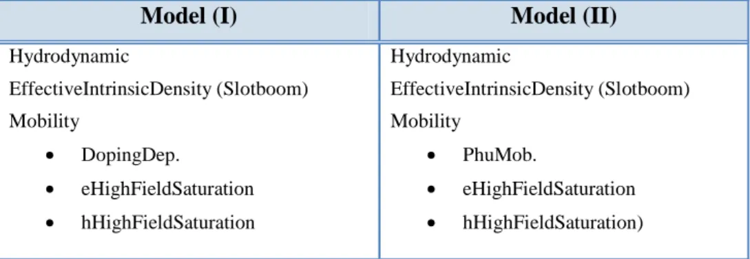
3.2 Transport Models ...81
3.2.1 Drift-Diffusion Model (DD)...81
3.2.2 Hydrodynamic Model (HD) ...81
3.3.1 SRH-Recombination Model ...83
3.3.2 Auger Recombination Model ...85
3.4 Mobility Models...85
3.4.1 Philips Unified Mobility Model ...86
3.4.2 High Field Saturation Model ...87
3.5 Mobility Models Under Stress ...88
3.5.1 Piezoresistance Mobility Model ...88
3.5.2 Stress-Induced Electron Mobility Model ...88
3.6 Band Structure Models...90
3.6.1 Bandgap Narrowing ...90
3.6.2 Intrinsic Density ...90
3.6.3 Effective Density-of-States ...91
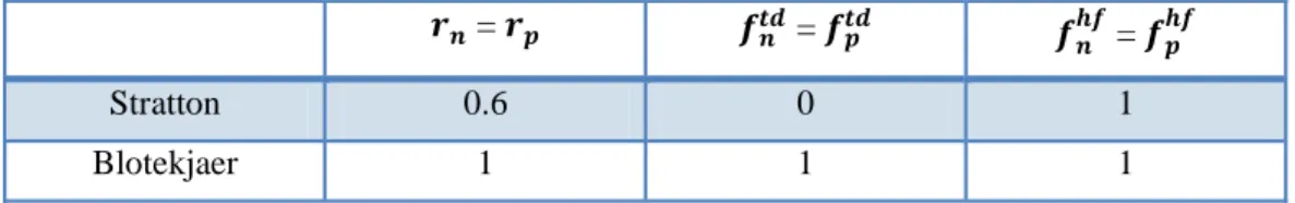
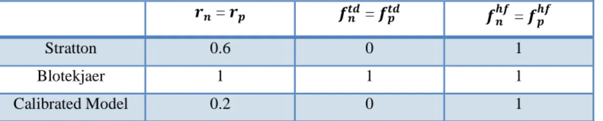
4. TCAD Calibration ...92
4.1 Mobility Models Calibration...92
4.2 Transport Models Calibration ...96
4.3 IMEC Structure ...102
5. Conclusion...104
References ...106
CHAPTER 4: TCAD Simulation Results...108
Strain Technology at the Base Region ...109
1. NPN-Si-BJT Device with Extrinsic Stress Layer...109
1.1 Impact of Strain...113
1.2 Electrical Simulation...114
1.3 Conclusion ...117
2. NPN-SiGe-HBT Device with Extrinsic Stress Layer...118
2.1 Impact of strain ...120
2.3 Conclusion ...125
Strain Technology at the Collector Region ...126
3. NPN-SiGe-HBT Device Employing Si3N4Strain Layer ...126
3.1 Process Simulation and Device Structure ...127
3.2 Impact of Strain...131
3.3 Electrical Simulation...132
3.4 Conclusion ...140
4. NPN-SiGe-HBT Device Employing SiO2Strain layer ...141
4.1 Impact of Strain...145
4.2 Electrical Simulation...146
4.3 Conclusion ...152
References ...153
Summary & Conclusion...155
Future work ...158
Appendix ...159
1. Mobility Models Calibration ...159
Abstract
The Impact of strain engineering technology applied on NPN-Si-BJT/NPN-SiGe-HBT devices on the electrical properties and frequency response has been investigated. Strain engineering technology can be used as an additional degree of freedom to enhance the carriers transport properties due to band structure changes and mobility enhancement. The mobility of charge carriers in bipolar devices can be enhanced by creating mechanical tensile strain in the direction of electrons flow to improve electron’s mobility, and by creating mechanical compressive strain in the direction of holes flow to improve hole’s mobility. Consequently, new devices concepts and novel device architectures that are based on strain engineering technology have been explored using TCAD modeling. The physical models and parameters used in TCAD simulations have been calibrated in collaboration with Bundeswehr University-Munich using Monte Carlo simulation. Specific models for SiGe bandgap, bandgap-narrowing, effective mass, energy relaxation, mobility for hydrodynamic and drift-diffusion simulations have been calculated and implemented in the house simulator using tabulated models compiled in C code. Two approaches have been used in this study to generate the proper mechanical strain inside the device. The first approach was through introducing strain engineering technology principle at the device’s base region using SiGe extrinsic stress layer. The second approach was through introducing strain engineering technology principle at the device’s collector region using strain layers. The study examined not only the transistor DC performance but also the RF performance through multiple optimizations for the explored vertical transistors. Simulation results showed that the strained silicon BJT/HBT devices exhibited better DC performance and high frequency characteristics in comparison with equivalent standard conventional BJT/HBT devices. An approximately 42% improvement in fTand 13% improvement in fMAXhave been achieved for BJT device employing
strain at the base region. As well, an enhancement of the collector current by nearly three times in strained silicon BJT device has been attained. The obtained results for applying the same
technique on NPN-SiGe-HBT device have shown that applying strain on the base region of the HBT device is less efficient in comparison with the BJT device, as the SiGe base is already stressed due to the existence of Ge at the base. Moreover, utilizing a strain layer at the device’s collector region will result in an approximately 9%-14% improvement in fT and 7%-12%
improvement in fMAX in comparison with an equivalent standard conventional NPN-SiGe-HBT
device. Despite of the very small decrease in the breakdown voltage BVCE0value (1% 4%), the
fT×BVCE0 product enhancement is about 12% by means of strain engineering at the collector
Résumé
Dans le but d’améliorer les transistors bipolaires TBH SiGe, nous proposons d’étudier l’impact de la contrainte mécanique sur leurs performances. En effet, cette contrainte permet de libérer un degré de liberté supplémentaire pour améliorer les propriétés du transport grâce à un changement de la structure de bande d’énergie du semiconducteur. Ainsi, nous avons proposé de nouvelles architectures de composants basées sur l’ingénierie de la contrainte mécanique dans les semiconducteurs. Deux approches ont été utilisées dans cette étude pour générer la tension mécanique adéquate à l'intérieur du dispositif. La première approche consiste à appliquer une contrainte mécanique sur la base du transistor en utilisant une couche de SiGe extrinsèque. La seconde approche vise à appliquer une contrainte dans la région du collecteur en utilisant une couche contrainte. Les résultats obtenus montrent que cette méthode peut être une approche prometteuse pour améliorer les performances des TBH.
CHAPTER 1
Introduction & Background
1.
Motivation
For the last two decades BiCMOS technology has been the dominant technology for analog RF high speed applications, due to the high linearity, high current drive capability, the lower 1/f noise, high output resistance, and voltage capability of the SiGe HBT. HBT has been a key device in this branch of semiconductor industry. However, due to the continuous demand for devices having higher frequency response, it becomes imperative to develop new bipolar architectures suitable for high frequency and power applications. Various techniques and efforts have been proposed to improve the performance of bipolar devices: introduction of a grading germanium into the base [1], introduction of carbon to improve 1D doping profile [2] and reduction of emitter width [3]. An additional way to improve the device performance is to enhance the carrier transport by changing the material properties. In advanced semiconductor devices strain can be used as an additional degree of freedom to enhance transport properties due to band structure changes [4]. Mobility of charge carriers in a bipolar device can be increased by creating mechanical tensile strain in the device in the direction of electrons flow to improve electron’s mobility, and by creating mechanical compressive strain in the device in the direction of holes flow to improve hole’s mobility [5].
The main motivation of this thesis is to clarify the impact of strain engineering technology on NPN-SiGe-HBT device’s electrical properties and frequency response, through exploring new device concepts and proposing new device’s architectures that are based on strain engineering
technology, and investigating the feasibility of such concepts in an industrial environment. These new concepts have been studied using finite element simulation TCAD tools.
The work methodology consists of the following steps:
Virtually fabricate the device using process simulations. Study the sensitivity of the device’s different zones to strain.
Propose new methods to incorporate strain in the process and evaluate the strain level that can be obtained inside the device.
Define simulation parameters and physical models (the model parameters have been calibrated in collaboration with Universität der Bundeswehr München).
Perform numerical (device) simulations to analyze the device electrical performance.
2.
Thesis Organization
The thesis is organized as follows:
Chapter 1: Introduction & Background; provides a brief discussion of the SiGe HBT
technology, theoretical background, state-of-the-art and the motivation for carrying out this research.
Chapter 2: Strain Technology; gives an overview of the elasticity theory of solids, physics
behind strain, different strain types, and application techniques of strain.
Chapter 3: TCAD Simulation & Modeling; provides an overview of the Technology Computer
Aided Design (TCAD), process simulation, device simulation and the physical models used in this study.
Chapter 4; TCAD Simulation Results; gives a detailed discussion of the approaches used to
create the desired mechanical strain inside the device, the devices architectures and the obtained results.
3.
Principles of SiGe-HBT
The fundamental advantage of SiGe HBT over conventional Si BJT arises from the bandgap engineering technology principle. Bandgap engineering technology can be used to improve several key figure-of-merits for a bipolar transistor. The first step in understanding how a heterostructure device operates is to consider the energy band diagram. The energy band diagram for a forward biased ideal graded-base SiGe HBT with constant doping in the emitter, the base and the collector regions, and a comparable Si BJT are shown in Fig.1. The Ge content is linearly graded from 0% near the metallurgical emitter–base (EB) junction to some maximum value of Ge content near the metallurgical collector–base (CB) junction, and then rapidly ramped back down to 0% Ge [6].
Fig.1: Energy band diagram for a graded-base SiGe HBT and a Si BJT.
The effect of introducing a graded Ge profile into the base region is apparent in the band structure changes shown above, where Eg,Ge(x = 0) and Eg,Ge(x = Wb) represent the
induced bandgap narrowing at the emitter end of the base (x = 0) and the germanium-induced bandgap narrowing at the collector end of the base (x = Wb), respectively. As shown in
the figure, a slight reduction in the base bandgap at the EB junction and a much larger reduction at the CB junction are observed with respect to the Si BJT device.
To illustrate the heterojunction action in a bipolar transistor, the operation of a conventional Si BJT will be considered first. When VBE is applied to forward bias the EB
junction, electrons are injected from the electron-rich emitter into the base across the EB potential barrier. The injected electrons diffuse across the base, and are swept into the electric field of the CB junction, yielding a useful collector current. At the same time, the applied forward bias on the EB junction produces a back-injection of holes from the base into the emitter. If the emitter region is heavily doped with respect to the base, the density of back-injected holes will be small compared to the forward-injected electron density, and hence a finite current gain results.
The introduction of Ge into the base region will affect the dc and ac operations of the Si BJT device. The reduction of the potential barrier to injection of electrons from emitter into the base will yield exponentially more electron injection for the same applied VBE, translating into
higher collector current, and hence higher current gain. In addition to that, the presence of a finite Ge content at the CB junction will positively influence the output conductance of the transistor, yielding higher Early voltage. For ac operation, the Ge-gradient-induced drift field across the neutral base will accelerate the injected minority electrons across the base, and thereby decreasing the base transit time. In what follows, the underlying physics of the NPN-SiGe-HBT, with particular emphasis on the fundamental differences between the operations of the SiGe HBT and the Si BJT will be introduced. For analysis purposes, a SiGe HBT and a Si BJT are taken to be of identical geometry, with identical emitter, base and collector-doping profiles, apart from the Ge in the base of the SiGe HBT. The Ge profile is assumed to be linearly graded from the EB to the CB junction as depicted in Fig.1. This analysis assumes standard low injection conditions, negligible bulk and surface recombination and Boltzmann statistics.
3.1 Current Gain
Due to the introduction of Ge into the base region, the potential energy barrier in the conduction band at the EB junction is lowered allowing more electrons to be injected into the base and thereby leads to an increase in the collector current. Furthermore, hole back injection is also reduced by the large valence band discontinuity reducing the base current. Overall, this increase in the collector current dramatically improves the current gain. For a constant base doping profile, the collector current density (JC) can be derived from the generalized Moll-Ross
J = q(e P (x)dx/ 1) D (x)n (x)
1.1 where Wbis the neutral base width for the applied bias VBE, Pb(x) is the base doping, Dnbis the
minority electron diffusivity in the base and nibis the intrinsic carrier density.
For SiGe HBT the intrinsic carrier density can be written as
n (x) = n e / e , ( ) , ( ) /( )e , ( )/ 1.2
Where E is the heavy-doping induced apparent bandgap narrowing in the base region, E , (0) is the Ge-induced band offset at x=0, E , (W ) is the Ge-induced band offset at
x=Wb, niois the low-doping intrinsic carrier density for Si, and is the effective density-of-states
ratio between SiGe and Si
=(( )) < 1 1.3
where (NCNV)SiGerepresents the position-dependent Ge-induced changes associated with both the
conduction and valence band effective density-of-states. The collector current density for SiGe HBT can be written as
J , =N W eqD / 1 n e / , ( )/
, ( )/
1 , ( )/ 1.4
where, is the minority electron diffusivity ratio between SiGe and Si, and is given by
= D( ) 1.5
The first term in Equation 1.4 corresponds to the Si BJT ,and the second term represents the modification of JC due to the introduction of Ge into the base region. As shown in the
equation, JCin a SiGe HBT depends exponentially on the EB boundary value of the Ge-induced
band offset, and is linearly proportional to the Ge-induced bandgap grading factor. Consequently, The SiGe HBT exhibits higher collector current and approximately the same base current as the Si BJT. This increase in JC for the SiGe HBT will lead to an increase in current gain. For
identically constructed devices, the ratio of the current gain ( ) between a linearly graded germanium profile SiGe HBT and a Si BJT is given by
,
, =
, ( )/ , ( )/
1 , ( )/ 1.6
Equation 1.6 represents a ratio which is larger than unity for a finite Ge content, and indicates that the smaller base bandgap in a SiGe HBT exponentially increases the number of minority carriers injected into the base, causing an increase in the collector current for the same forward-bias, and hence higher current gain value.
3.2 Early Voltage
The most important physical effect which causes the collector current to increase with the collector-emitter voltage for a constant base current is the increase of collector current caused by a decreased neutral base width with base-collector reverse bias (VCB). The output conductance is
a measure of collector current variation with VCB. Therefore, low output conductance is desirable
to achieve invariant output current in low-frequency analogue applications. The Early voltage (VA) is a measure of the change in output conductance with changing VCB. For analogue circuit
applications, a high value of the product of current gain and Early voltage is desirable, which is conventionally defined as the figure-of-merit for analog circuit design.
An additional benefit of using a graded-Ge profile in a SiGe HBT is the enhancement of the Early voltage. The enhancement of the Early voltage of a graded SiGe HBT can be expressed as , , | exp , ( ) kT 1 , ( )/ , ( )/ 1.7
This ratio is larger than unity, and it indicates that for a finite grading across the quasi-neutral base, the exponential dominates the functional dependence on Ge content, yielding an improvement for a SiGe HBT compared to a Si BJT.
3.3 Transit Time
As a result of the quasi-electric field due to the grading of the Ge content in the base, the electrons injected from the emitter to the collector will be accelerated; thereby effectively reducing the base transit time. For bipolar transistors, the base transit time for a constant base doping is given by
= n (x)P (x) D (y)n (y)P (y)dy dx 1.8
By substituting equation 1.2 into equation 1.8 and integrating, the SiGe HBT transit time becomes
, =DW kT
, ( ) 1 , ( ) 1
, ( )/ 1.9
For Si BJT, the base transit time is given by
, =2DW 1.10
Hence, the enhancement of the base transit time due to the existence of a graded Ge profile into the base region is given by ratio of the base transit time for SiGe ( , ), and Si BJT ( , ) as follows , , = 2 , ( ) 1 , ( ) 1 , ( ) 1.11 For a finite Ge grading, the ratio ( , / , ) will be less than unity, and therefore the SiGe HBT base transit time will be shorter than Si BJT.
Moreover, the forward bias in EB junction creates a back-injection of holes from the base to the emitter, and gives rise to emitter charge storage delay time ( ). The emitter charging time will be reduced due to the lower barrier which carriers must overcome before being injected into the base due to the existence of the graded Ge profile at the base region.
3.4 High Frequency Figures-of-Merit
The SiGe base gives new degrees of freedom for the design of SiGe HBTs and allows much higher values of the figures of merit; the cut-off frequency (fT) and the maximum
oscillation frequency (fMAX), to be achieved in comparison with the conventional silicon BJTs.
The unity-gain cut-off frequency and the maximum oscillation frequency parameters are positively impacted by the Ge content in the base. As mentioned previously and decrease in SiGe HBT.
The unity-gain cutoff frequency (fT) is given by the relation
=21 q ( + ) + + +
2 + 1.12
Where Icis the collector current, CEBand CCBare the EB and CB depletion capacitances, WCBis
the CB space-charge region width, vsatis the saturation velocity, and rcis the dynamic collector
resistance. Therefore, improvements in and due to the presence of SiGe will directly translate into an enhanced fTof the transistor at fixed bias current. The maximum oscillation
frequency (fMAX) figure of merit is defined as
= 8 1.13
Where rB is the base resistance. Therefore, the increase in fT and the reduction in the base
resistance aids in improving the fMAXof the SiGe HBT [7] [8].
4.
State-of-the-Art
The design and study of a new semiconductor device structure hold promise at both the device level, where the transistor’s electrical behavior may lead to novel effects, and the circuit level, where the device characteristics may be exploited to enhance functional performance. Since the revolutionary invention of the point-contact transistor at Bell Laboratories in 1947, the progress made in the field of semiconductor technology have a constant increase in performance according to Moore’ law which states that the number of transistors per chip doubles every 18-24
months. However, as silicon BJTs reach their fundamental limits on speed because of the physical properties of the semiconductor material, advanced high-speed devices require heterojunction technology. The idea of varying the bandgap in a bipolar transistor structure to increase the emitter injection efficiency is almost as old as the bipolar junction transistor itself. Shockley described the idea in his application for a patent on the junction bipolar transistor [9][10]. The inherent performance advantages of heterojunction bipolar transistors (HBTs) over conventional bipolar junction transistors have been recognized, and Kroemer first explained the underlying principle of the heterojunctions in 1957 [11].
The work by Kroemer on the heterojunction opened a new door for achieving higher speeds than anticipated with silicon bipolar transistors. Although the performance advantages of HBTs over BJTs were well understood, no fabrication technologies were available to produce high quality heterojunctions until the 1970s, where epitaxial growth of SiGe heterostructures demonstrated by Erich Kasper using molecular beam epitaxy (MBE) [12]. With the advent of heteroepitaxy, the concept of strained layers has been extended to include other elemental semiconductors. These developments set the stage for IBM’s development of SiGe HBTs in 1987 using MBE. The successful demonstrations of SiGe HBT technology, in both high-performance digital and analogue circuit applications, are the results of over 15 years of steady research progress from initial material preparations in 1984, through device demonstrations from 1987– 1992 to large scale circuit fabrication in 1994 and commercial products in 1998. Since then, the interest in SiGe HBTs from both academia and industry rose progressively through the years causing the figures of merit to increase and reach current the-art levels. Today’s state-of-the-art SiGe pre-production technologies have shown cut-off frequency close to 300 GHz, and maximum frequency of oscillation close to 400 GHz as reported recently by our partners of the European joint research project DOTFIVE [13] [14].
The rapid improvement in SiGe HBT performance is mainly due to careful tailoring of Ge and doping profiles, and also due to the continuing downscaling of device dimensions. Material growth development is also an important factor for the success of SiGe technology and the most recent example is the incorporation of carbon in the SiGe epitaxial layers, which further improves performance. The developments of SiGe HBTs technology are summarized in Table.1 [7].
Historical Event Year Ref.
First demonstration of transistor action 1947 [15]
Basic HBT concept 1948 [9]
First demonstration of a bipolar junction transistor 1951 [10]
First demonstration of a silicon bipolar transistor 1956 [16]
Drift-base HBT concept 1954 [17]
Fundamental HBT theory 1957 [18][11]
First epitaxial silicon transistors 1960 [19]
First SiGe HBT 1987 [20]
First ideal SiGe HBT grown by CVD 1989 [21]
First SiGe HBT grown by UHV/CVD 1989 [22]
First high-performance SiGe HBT 1990 [23][24]
First self-aligned SiGe HBT 1990 [25]
First SiGe HBT ECL ring oscillator 1990 [25]
First pnp SiGe HBT 1990 [26]
First operation of SiGe HBTs at cryogenic temperatures 1990 [27]
First SiGe HBT BiCMOS technology 1992 [28]
First LSI SiGe HBT integrated circuit 1993 [29]
First SiGe HBT with peak fTabove 100 GHz 1993 [30][31]
First SiGe HBT technology in 200-mm manufacturing 1994 [32]
First SiGe HBT technology optimized for 77K 1994 [33]
First radiation tolerance investigation of SiGe HBTs 1995 [34]
First report of low-frequency noise in SiGe HBTs 1995 [35]
First SiGe:C HBT 1996 [36]
First high-power SiGe HBTs 1996 [37][38]
First sub-10psec SiGe HBT ECL circuits 1997 [39]
First high-performance SiGe:C HBT technology 1999 [40]
First SiGe HBT with peak fTabove 200 GHz 2001 [41]
First SiGe HBT with peak fTabove 300 GHz 2002 [42]
First complementary (npn+pnp) SiGe HBT technology 2003 [43]
First C-SiGe technology with npn and pnp fTabove 100 GHz 2003 [44]
First vertical SiGe HBT on thin film (CMOS compatible) SOI 2003 [45]
First SiGe HBT with both fTand fMAXabove 300 GHz 2004 [46]
First Conventional Double-Polysilicon FSA-SEG Si/SiGe:C HBT with fMAX423 GHz and fT273 GHz
2009 [14]
First Fully Self-Aligned SiGe:C HBT Architecture with fMAX400 GHz 2009 [13]
First SiGe HBT with fMAX500 GHz (IHP: to be published in IEDM 2010) 2010
4.1 Strained SiGe HBT
Due to the continuous demand for devices having higher frequency response, it becomes imperative to develop new bipolar architectures suitable for high frequency and power applications. Therefore, various efforts and approaches have been proposed to improve the bipolar devices performance. In advanced semiconductor devices technology, strain engineering technology is considered as an additional degree of freedom to enhance transport properties due to band structure changes. Recent experimental and theoretical work point out uniaxially and biaxially stressed Si and SiGe substrates as a possible technique for the new generation HBT devices. Experimentally, two major methods have been used; wafer bending [47], and virtual substrates [48]. Wafer bending allows inducing uniaxial stress while virtual substrates create biaxial stress. Both methods induce a uniform stress over the device. In what follows, a brief description of the latest work done on strained SiGe HBTs using wafer bending and virtual substrate approaches is presented.
Wang et al. investigated the impact of mechanical uniaxial stress on the characteristics of SiGe heterojunction bipolar transistors uing a four-point bending apparatus to apply a uniaxial stress in the range of 200 MPa to + 200 MPa. The SiGe HBTs used in their study were fabricated using 0.18 µm self-aligned SiGe BiCMOS technology, with an emitter area of 0.2x10.16 µm2. Their results show that the performances of SiGe HBTs are varied with the stress level. The changes in the collector current, base current, current gain, and the breakdown voltage were found to be linearly dependent upon the mechanical uniaxial stress level, for the range of 200 MPa to + 200 MPa. The strain-polarity dependence of the collector current, base current, and current gain was positive under uniaxial compressive stress, whereas that of the breakdown voltage was negative [47].
Yuan et al. in their work reported the performance of Si–SiGe HBT under the biaxial compressive and tensile mechanical stress with the comparison of BJTs. An externally uniform mechanical displacement at the center with the diameter of 13 mm on 100 mm wafers for both SiGe HBT and Si BJT devices has been applied as shown in Fig.2. The average biaxial strain used in this study is 0.028%. The current gain variations of the mechanically strained Si–SiGe heterojunction bipolar transistor (HBT) and Si bipolar junction transistor (BJT) devices were investigated. The current gain change for HBT is found to be 4.2% and 7.8% under the biaxial compressive and tensile mechanical strain of 0.028%, respectively. The change for BJT is found
to be 4.9% and 5.0% under the biaxial compressive and tensile mechanical strain of 0.028%, respectively. Their results are shown in Fig.3 . Moreover, their results show that the current gain changes show a good linear dependence on external biaxial mechanical stress as shown in Fig.4 [49].
Fig.2 : Schematic diagram of the externally applied mechanical stress on the wafer.
Persson et al. [48] reported in their work (Fabrication and characterization of strained Si heterojunction bipolar transistors on virtual substrates), a strained Si HBT with a maximum current gain of 3700 using a relaxed Si0.85Ge0.15virtual substrate, Si0.7Ge0.3base and strained Si
emitter. The schematic of the complete structure used in their study is shown in Fig.5. Their
Fig.3: Gummel plot of Si BJT and SiGe HBT devices without and with mechanical stress (VBC=0 V).
Fig.4: Current gain changes of SiGe HBT and Si BJT device as a function of stress level.
results demonstrate major improvements in current gain compared with co pseudomorphic SiGe HBTs and Si BJTs as shown in
larger collector current than SiGe HBT and Si BJTs
Fig.5: A schematic of the complete strained Si HBT structure used
Fig.6: Collector current (IC) vs. collector
voltage (VCE) characteristics for strained Si HBT,
SiGe HBT, and Si BJT at I
Haugerud et al. studied the effects of mechanical planar biaxial tensile strain applied, post-fabrication, to Si/SiGe HBT BiCMOS technology. Planar biaxial tensile strain was applied to the samples, which included standard Si CMOS, SiGe HBTs, and a
control. Their results show that a
consistent decrease in collector current and hence current gain after strain as
results demonstrate major improvements in current gain compared with co
pseudomorphic SiGe HBTs and Si BJTs as shown in Fig.6. In addition, strained Si HBTs exhibit than SiGe HBT and Si BJTs as shown in Fig.7.
schematic of the complete strained Si HBT structure used by
vs. collector-emitter characteristics for strained Si HBT, SiGe HBT, and Si BJT at IB= 3 A.
Fig.7: Current gain vs. base
is increased by almost one order of magnitude in the strained Si HBT.
Haugerud et al. studied the effects of mechanical planar biaxial tensile strain applied, fabrication, to Si/SiGe HBT BiCMOS technology. Planar biaxial tensile strain was applied to the samples, which included standard Si CMOS, SiGe HBTs, and an epi
Their results show that at a strain level of 0.123%, the Si BJT/SiGe HBTs showed a consistent decrease in collector current and hence current gain after strain as
results demonstrate major improvements in current gain compared with co-processed . In addition, strained Si HBTs exhibit
Persson et al.
vs. base-emitter voltage VBE.
is increased by almost one order of magnitude in the strained Si HBT.
Haugerud et al. studied the effects of mechanical planar biaxial tensile strain applied, fabrication, to Si/SiGe HBT BiCMOS technology. Planar biaxial tensile strain was applied n epitaxial-base Si BJT he Si BJT/SiGe HBTs showed a consistent decrease in collector current and hence current gain after strain as illustrated in Fig.8
and Fig.9. This decrease in the collector current is attributed to the compressive strain in the orthogonal plane which degrades the electron transport [50].
Fig.8: Forward Gummel characteristics of a first generation SiGe HBT for both pre-strain and post
0.123% biaxial strain.
Fig.9: Output characteristics of a first generation SiGe HBT for both pre-strain and post 0.123%
biaxial strain
Moreover, two patents have been proposed to introduce stress into bipolar transistors: The first patent by Chidambarrao et al. proposes to create stress at the base region of the device as shown in Fig.10. In their structure, the compressive and tensile strains are created by forming a stress layer in close proximity to the intrinsic base of the device resulting in an enhancement of the mobility of the charge carriers [51]. The second patent by Dunn et al. proposes a method of forming a semiconductor device having two different strains inside the device [52]. This proposal is more complicated since the stress is applied on the emitter, the base and the collector regions as shown in Fig.11.
To the best of our knowledge, there haven't been any simulation or measurement results available in the literature to evaluate the effect of the stress layers in the above structures, thus we have analyzed the impact of strain engineering on SiGe-HBTs via modified ideas from the above patents using a specific structure provided by IMEC Microelectronic-Belgium as a reference device [53].
Fig.10: A cross- sectional view of a complete BJT device formed according to Chidambarrao et al.
Fig.11: A cross- sectional view of a complete BJT device formed according to Dunn et al.
Regarding the theoretical work done in this field, Jankovic et al. investigated the influence of strained-Si cap layers on n–p–n heterojunction bipolar transistors fabricated on virtual substrates as shown in Fig.12. Using an approximate theoretical model, they found that the presence of a strained-Si/SiGe (relaxed) heterojunction barrier in the emitter can substantially improve the HBT’s current gain as shown in Fig.13. Furthermore, two-dimensional numerical simulations of a virtual substrate HBT with a realistic geometry demonstrate that, besides the current gain enhancement, a three times improvement in fT and fMAX were realized when a
strained-Si/SiGe emitter is incorporated as shown in Fig.14 and Fig.15.
Moreover, Jankovic et al. presented a computational study by commercial TCAD of the potential electrical and thermal properties of n–p–n HBTs fabricated on relaxed Si1-yGey virtual
substrates. The dependences of dc, ac and self-heating characteristics of virtual substrate HBTs (VS HBTs) on alloy composition were investigated in details. It is found that symmetrical VS HBTs generally exhibit higher current drive capabilities compared with equivalent HBTs formed pseudomorphically on Si substrates, but at the expense of a lower fT and a decreased fMAX. In
addition, simulated results show that self-heating effects become increasingly significant for VS HBTs, substantially degrading device electrical parameters such as the early voltage [54] [55].
E B C STI STI STI Stress layer C B E Strain film Strain film
Fig.12: 2D cross-section of the simulated virtual substrate HBT device with strained-Si/SiGe
heterointerface emitter
Fig.13: the (Ic) characteristics of virtual substrate HBTs with thin (10 nm), thick (50 nm) and without
strained-Si layers in the emitter
Fig.14: fTversus collector current Ic extracted for
the n p n HBTs with and without strained-Si cap layer and for conventional silicon-based HBT.
Fig.15: fMAXversus collector current Ic extracted
for the n p n HBTs with and without strained-Si cap layer and for conventional silicon-based HBT.
Simulation results reported by Jankovic et al. show optimistic improvements of the HBT deice performance by means of strain engineering technology. As they are using an approximate theoretical model in their simulations, this approximate theoretical model might need to be calibrated and/or taking more effects in consideration to achieve more precise results.
4.2 Current State-of-the-Art
As mentioned previously, the European joint research project DOTFIVE partners have achieved SiGe:C HBTs with maximum frequency of oscillation (fMAX) 400 GHz which are
today’s state-of-the-art SiGe:C HBTs. These partners achieve this milestone through completely different architectures. The first partners (IMEC & IHP Microelectronics) approache 400 GHz fMAX through fully self-aligned (FSA) SiGe:C architecture. While the second partner (ST
Microelectronics) approaches 400 GHz fMAX through a conventional double-polysilicon FSA
selective epitaxial growth (SEG) Si/SiGe:C HBT. In what follows a brief description of each approach is given.
IMEC and IHP have developed two novel device architectures for half terahertz RF performance to reduce further the device parasitic elements compared to the reference quasi self-aligned (QSA) architecture (fT = 205 GHz, and fMAX= 275 GHz ). The first architecture named
G1G architecture is the novel FSA IMEC architecture. The second architecture is the novel FSA IHP architecture. The novel device architecture that IMEC explores, attempts to reduce the device parasitics significantly. The key element to achieve this, is that the emitter, base and collector regions are self-aligned to each other. This is accomplished by growing the collector/base and capping layer non-selectively, then etching the extrinsic device region away using a sacrificial emitter, and then using the sacrificial emitter to self-align a reconstructed external base to the emitter region. Initial results with this approach yielded marginal devices with poor performance. But the concept to fabricate such a device was demonstrated, and as the reasons for the poor performance and process marginalities were identified, IMEC continued to optimize this architecture in the frame of the DOTFIVE project. A schematic cross-section of the novel FSA IMEC device architecture is shown in Fig.16.
IMEC started from an initial process flow, which yielded marginally functional devices with fMAX below 200 GHz. This initial process flow has been completely reviewed, and the unit
process steps have been significantly improved. A SEM cross-section showing the device architecture after the unit process step improvements, compared to the original structure is shown in Fig.17. The major deficiencies of the original structure have been alleviated, such as the marginal thickness of the external base connection, the marginal overlap of the polyemitter over the L-shaped spacer, the marginal L-shaped spacer formation, and the sloped profile of the pedestal etch. The resulting device has an effective emitter width of 80nm.
This fully self-aligned SiGe:C HBT architecture featuring a single step epitaxial collector/base process, removal of the extrinsic part of the device using sacrificial emitter, external base reconstruction, L-shaped spacer formation after removal of the sacrificial emitter, and in-situ As doped polyemitter demonstrated 400 GHz fMAX. In addition, introducing carbon in
the collector suppressed segregation of P in the collector to the Si/SiGe interface, which resulted in a strong increase of the fMAXbecause of the reduction of CBC. The resulting fTand fMAXcurves
are shown in Fig.18, and the base-collector reverse diode current is shown in Fig.19. The influence of the addition of 0.2% carbon to the undoped collector part is demonstrated. This improvement is the accumulated result of a further lateral scaling of the HBT device, a significant decrease of the base resistance and of the base-collector capacitance compared with the reference HBT device.
Fig.18: Base-collector reverse diode current for a 0.15x1.0 m2HBT device
Fig.19 :fTand fMAXversus Ic for a 0.15x1.0 m
2
HBT.
Regarding the IHP novel architecture, a new collector construction for high-speed SiGe:C HBTs that substantially reduces the parasitic base-collector capacitance by selectively under etching the collector region is presented. A schematic cross-section of the novel IHP device architecture is shown in Fig.20. The IHP novel architecture provides fT values that are higher
compared to the G1G architecture and presents less variation with decreasing emitter width. The CBEand REvalues of the IHP architecture are lower than the G1G architecture helping to obtain
higher fTvalues. The fMAXvalues for both architectures show a similar increase with decreasing
the emitter width. The IHP architecture however provides slightly lower fMAX values at wider
emitter widths while the situation reverses for the smallest simulated dimensions [13] [56].
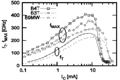
On the other hand, ST Microelectronics approaches 400 GHz fMAXthrough a conventional
double-polysilicon FSA selective epitaxial growth (SEG) Si/SiGe:C HBT. Starting from the high speed SiGe BiCMOS technology BiCMOS9MW ( Fig.21) which features a SA selective epitaxial SiGe HBT with 230 GHz / 290 GHz fT / fMAX, two shrinking phases (B3T and B4T) have been
performed by STMicroelectronics. The path followed to move from a 300 GHz fMAX HBT
(BiCMOS9MW) to a 400 GHz fMAXHBT (B4T) is shown in Fig.22.
Fig.21: Sketch of the FSA-SEG SiGe HBT architecture
Fig.22 : From BiCMOS9MW to B4T: Splits of the vertical and lateral scaling contributions.
The vertical shrink V1 corresponds to a slight reduction of the spike annealing temperature, a different base profile and a reduction of the collector doping. Lateral shrink L1 corresponds to a reduction of the collector area, the polyemitter and emitter inside spacer widths, the final emitter width being unchanged (0.13µm). The result of this first shrinking phase is a technology called B3T, featuring fT = 260 GHz and fMAX= 350 GHz. Using still a conventional
SA selective epitaxial base HBT, a second shrinking phase resulted in the B4T technology providing a maximum oscillation frequency of 400 GHz together with a transit frequency of 265 GHz (wafer averages). These outstanding performance data have been obtained for a collector base breakdown voltage of 6.0 V and a collector emitter breakdown voltage of 1.5 V (WE is
reduced to 0.11 µm for the lateral shrink L2). The fTand fMAXcharacteristics versus collector
current of a B4T transistor, compared to those of B3T and BiCMOS9MW HBTs having the same drawn emitter window length are shown in Fig.23. Moreover the main electrical parameters of these devices are summarized inTable 2[14] [56].
Fig.23: fT& fMAXvs. ICfor BiCMOS9MW, B3T and B4T technologies at VCB= 0.5 V (LE~ 5 m). Parameter Measurements conditions BiCMOS9MW B3T B4T Unit fT VCB=0.5 V 230 260 265 GHz fMAX VCB=0.5 V 290 350 400 GHz WE TEM 0.13 0.13 0.11 µm JC Peak fT 15.0 11.8 13.0 mA/µm 2 VBE=0.75V 950 1595 1750 -VAF >200 >200 >200 V BVEBO 2.2 2.1 2.1 V BVCEO VBE=0.7V 1.5 1.55 1.50 V BVCBO 5.5 6.0 6.0 V RBi 2.7 2.5 2.5 k
Table 2: HBT parameters comparison (wafer averages) FOR BICMOS9MW, B3T and B4T technologies (LE~5µm).
However, IHP Microelectronics reached a SiGe HBT device with fT/fMAXof 300 GHz/500
GHz, their results will be published in IEDM 2010 proceedings. The speed-improvement compared to previous SiGe HBT technologies originates from the reduced specific collector-base capacitance and base resistance and scaling of the device dimensions.
5.
DOTFIVE Project
THz technology is an emerging field which has demonstrated a wide-ranging potential. Extensive research in the last years has identified many attractive application areas and has paved the technological path towards broadly usable THz systems. THz technology is currently in a pivotal phase and will soon be in a position to radically expand our analytic capabilities via its intrinsic benefits. In this context, DOTFIVE is planned to establish the basis for fully integrated cost efficient electronic THz solutions. An illustration of some exemplary applications of Terahertz radiation is shown in Fig.24.
Fig.24: Illustration of some exemplary applications of Terahertz radiation.
DOTFIVE is an ambitious three-year European project supported by the European Commission through the Seventh Framework Program for Research and Technological Development, focused on advanced Research, Technology, and Development activities necessary to move the SiGe-HBT into the operating frequency range of 0.5 THz (500 GHz). This high frequency performance is currently only possible with more expensive technology based on III-V semiconductors, making high integration and functionality for large volume consumer applications difficult. The new transistors developed by DOTFIVE will be used for designing circuits enabling power efficient millimeter-wave applications such as automotive radar (77 GHz)
or WLAN communications systems (60 GHz –Wireless Local Area Network). In addition to these already evolving markets, DOTFIVE technology sets out to be a key enabler for silicon based millimeter-wave circuits with applications in the security, medical and scientific areas. A higher operating speed can open up new application areas at very high frequencies, or can be traded for lower power dissipation, or can help to reduce the impact of process, voltage and temperature. The project involves 15 partners from industry and academia in five countries teaming up for research and development work on silicon-based transistor architectures, device modeling, and circuit design. The scientific aspects of the DOTFIVE project are tackled by five work packages during a period of 36 months as illustrated in the schematic shown in Fig.25.
Fig.25: DOTFIVE project work packages
The work of this thesis is a part of the work package1 (WP1) which is dedicated to “physics-based predictive modeling” using Technology Computer Aided Design (TCAD) tools, that allow the simulation of processing steps and electrical characteristics of devices. Due to the complexity of transport phenomena in nano-scale transistors, advanced device simulation tools (e.g., solution of Boltzmann transport, Schrödinger-Possion solver) from DOTFIVE partners are used. Based on such advanced TCAD platform, it will be possible to achieve a deep understanding of the electrical behavior of near-terahertz devices and to develop guidelines for doping and architecture optimization. In particular, WP1 will support continuously the technology development in WP2 and WP3 by, e.g., assessing the achievable performance limits, identifying the critical limitations, and exploring new device concepts and architectures. To make computationally more efficient drift-diffusion and energy-balance based simulators predictive for high performance devices, their physical models for, e.g., carrier transport are obtained from first principles solutions of the Boltzmann transport equation (BTE). Furthermore, WP1 will investigate the ultimate limits of SiGe HBT technology in terms of device performance, transport
limits, quantum effects, and safe operation area limitations [56]. The partners involved in this package are: University of Naples-Italy, ST France, IMEC Microelectronics-Belgium, IMS-University of Bordeaux 1-France and Bundeswehr University Munich-Germany.
References
[1] S.L. Salmon, J. D. Cressler, R. C. Jaeger, D. L. Harame, “The Influence of Ge Grading on the Bias and Temperature Characteristics of SiGe HBT’s for Precision Analog Circuits” vol. 47, 2000.
[2] B. Tillack, B. Heinemann, D. Knoll, H. Rücker, Y. Yamamoto, “Base doping and dopant profile control of SiGe npn and pnp HBTs” vol. 254, 2008.
[3] F. Ellinger, L. C. Rodoni, G. Sialm, C. Kromer, G. von Büren, M. Schmatz, C. Menolfi, T. Toifl, T. Morf, M. Kossel, H. Jäckel, “Effects of emitter scaling and device biasing on millimeter-wave VCO performance in 200 GHz SiGe HBT technology” vol. 52, 2004. [4] P.R. Chidambaram, C. Bowen, S. Chakravarthi,C. Machala, R. Wise, “Fundamentals of
silicon material properties for successful exploitation of strain engineering in modern CMOS manufacturing” vol. 53, 2006.
[5] J.L. Egley, D. Chidambarrao, “Strain effects on device characteristics: Implementation in drift-diffusion simulators” vol. 36, pp. 1653-1664, 1993.
[6] J. D. Cressler, Silicon heterostructure handbook. Taylor & Francis, 2006. [7] John D. Cressler, Silicon Heterostructure Devices. CRC Press, 2007. [8] P. Ashburn, SiGe Heterojunction Bipolar Transistors. Wiley, 2003. [9] “Circuit element utilizing semiconductive material” U.S. Patent 2569347.
[10] W. Shockley, M. Sparks, G.K. Teal, “p-n Junction Transistors” Physical Review, vol. 83, 1951.
[11] H. Kroemer, “Theory of a wide-gap emitter for transistor” Proceedings of the IRE, vol. 42, 1957.
[12] E. Kasper, H. J. Herzog and H. Kibbel, “A one-dimensional SiGe superlattice grown by UHV epitaxy” Applied Physics A: Materials Science & Processing, vol. 8, 1975.
[13] S. Van Huylenbroeck et al., “A 400GHz fMAX Fully Self-Aligned SiGe:C HBT
Architecture” Proceedings IEEE BCTM, p. 5, 2009.
[14] P. Chevalier et al., “A Conventional Double-Polysilicon FSA-SEG Si/SiGe:C HBT Reaching 400 GHz fMAX” Proceedings IEEE BCTM, p. 1, 2009.
[15] J. Bardeen, W.H. Brattain, “The transistor, a semi-conductor triode” Physical Review, vol. 71, 1947.
[16] M. Tanenbaum, D.E. Thomas, “Diffused emitter and base silicon transistors” Bell System
Technical Journal, vol. 35, 1956.
[17] H. Kroemer, “Zur theorie des diffusions und des drift transistors. Part III.” Archiv der
Elektrischen Ubertragungstechnik, vol. 8, 1954.
[18] H. Kroemer, “Quasielectric and quasimagnetic fields in nonuniform semiconductors” RCA
Review, vol. 18, 1957.
[19] H.C. Theuerer, J.J. Kleimack, H.H. Loar, and H. Christensen, “Epitaxial diffused transistors” Proceedings of the IRE, vol. 48, 1960.
[20] S.S. Iyer, G.L. Patton, S.L. Delage, S. Tiwari, and J.M.C. Stork, “Silicon–germanium base heterojunction\line bipolar transistors by molecular beam epitaxy” Technical Digest of the
IEEE International Electron Devices Meeting, San Francisco, 1987.
[21] C.A .King, J.L. Hoyt, C.M. Gronet, J.F. Gibbons, M.P. Scott, and J. Turner, “Si/Si1-x/Gex
heterojunction\line bipolar transistors produced by limited reaction processing” IEEE
Electron Device Letters, vol. 10, 1989.
[22] G.L. Patton, D.L. Harame, J.M.C. Stork, et al., “Graded-SiGe-base, polyemitter heterojunction bipolar transistors” IEEE Electron Device Letters, vol. 10, 1989.
[23] G.L Patton, J.H .Comfort, B.S. Meyerson, et al., “63-75 GHz fT SiGe-base
heterojunction-bipolar technology” Technical Digest IEEE Symposium on VLSI Technology, Honolulu,, 1990.
[24] G.L. Patton, J.H. Comfort, B.S.Meyerson, et al., “75 GHz fT SiGe base heterojunction
bipolar transistors” IEEE Electron Device Letters, vol. 11, 1990.
[25] J.H. Comfort, G.L. Patton, J.D. Cressler,et al., “Profile leverage in a selfaligned epitaxial Si or SiGe-base bipolar technology” Technical Digest IEEE International Electron Devices
Meeting, Washington, 1990.
[26] D.L. Harame, J.M.C. Stork, B.S. Meyerson, et al., “SiGe-base PNP transistors fabrication with n-type UHV/CVD LTE in a ‘‘NO DT’’ process” Technical Digest IEEE Symposium on
VLSI Technology, Honolulu, 1990.
[27] E.F. Crabbee´, G.L.Patton, J.M.C Stork, B.S. Meyerson, and J.Y-C Sun, “Low temperature operation of Si and SiGe bipolar transistors” Technical Digest IEEE International Electron
Devices Meeting, Washington, 1990.
[28] D.L.Harame, E.F. Crabbe´, J.D. Cressler, et al., “A high-performance epitaxial SiGe-base ECL BiCMOS technology” Technical Digest IEEE International Electron Devices Meeting,
Washington, 1992.
for high speed analog and mixed-signal applications” Technical Digest IEEE International
Electron Devices Meeting, San Francisco, 1993.
[30] E. Kasper, A. Gruhle, H. Kibbel, “High speed SiGe-HBT with very low base sheet resistivity” Technical Digest IEEE International Electron Devices Meeting, San Francisco, 1993.
[31] E.F Crabbe´, B.S. Meyerson, J.M.C. Stork, and D.L. Harame, “Vertical profile optimization of very high frequency epitaxial Si- and SiGe-base bipolar transistors” Technical Digest
IEEE International Electron Devices Meeting, Washington, 1993.
[32] D.L Harame, K. Schonenberg, M. Gilbert,, “A 200mm SiGe-HBT technology for wireless and mixed-signal applications” Technical Digest IEEE International Electron Devices
Meeting, Washington, 1994.
[33] J.D. Cressler, E.F. Crabbe´, J.H. Comfort, .JY-C Sun, and J.M.C Stork, “An epitaxial emitter cap SiGe base bipolar technology for liquid nitrogen temperature operation” IEEE
Electron Device Letters, vol. 15, 1994.
[34] J.A. Babcock, J.D. Cressler, L.S. Vempati, et al., “Ionizing radiation tolerance of high performance SiGe HBTs grown by UHV/CVD” IEEE Transactions on Nuclear Science, vol. 42, 1995.
[35] L.S. Vempati, J.D. Cressler, R.C. Jaeger, and D.L. Harame, “Low-frequency noise in UHV/CVD Si- and SiGe-base bipolar transistors” Proceedings of the IEEE BCTM,
Minnneapolis, 1995.
[36] L. Lanzerotti, A. St Amour, C.W. Liu, et al., “Si/Si1-x-yGexCy /Si heterojunction bipolar
transistors” IEEE Electron Device Letters, vol. 17, 1996.
[37] A. Schuppen, S. Gerlach, H. Dietrich, et al, “1-W SiGe power HBTs for mobile communications” IEEE Microwave and Guided Wave Letters, 1996.
[38] P.A. Potyraj, K.J. Petrosky, K.D.Hobart, et al, “A 230-Watt S-band SiGe heterojunction junction bipolar transistor” IEEE Transactions on Microwave Theory and Techniques, vol. 44, 1996.
[39] K. Washio, E. Ohue, K. Oda, et al., “A selective-epitaxial SiGe HBT with SMI electrodes featuring 9.3-ps ECL-Gate Delay” Technical Digest IEEE International Electron Devices
Meeting, San Francisco, 1997.
[40] H.J. Osten, D. Knoll, B. Heinemann, et al., “Carbon doped SiGe heterojunction bipolar transistors for high frequency applications” Proceedings of the IEEE BCTM, Minnneapolis, 1999.
[41] S.J. Jeng, B. Jagannathan, J-S.Rieh, et al., “A 210-GHz fT SiGe HBT with nonself- aligned
[42] J.S. Rieh, B. Jagannathan, H. Chen, et al., “SiGe HBTs with cut-off frequency of 350 GHz”
Technical Digest of the IEEE International Electron Devices Meeting, San Francisco, p.
2002.
[43] B. El-Kareh, S. Balster, W. Leitz, et al., “A 5V complementary SiGe BiCMOS technology for high-speed precision analog circuits” Proceedings of the IEEE BCTM, Toulouse, 2003. [44] B. Heinemann, R. Barth, D. Bolze, et al., “A complementary BiCMOS technology with high
speed npn and pnp SiGe:C HBTs” Technical Digest of the IEEE International Electron
Devices Meeting, Washington, 2003.
[45] J. Cai, M. Kumar, M. Steigerwalt, et al., “Vertical SiGe-base bipolar transistors on CMOS-compatible SOI substrate” Proceedings of the IEEE BCTM, Toulouse, 2003.
[46] J.S. Rieh, D. Greenberg, M. Khater, et al., “SiGe HBTs for millimeterwave applications with simultaneously optimized fT and fMAX” Proceedings of the IEEE Radio Frequency
Integrated Circuits (RFIC) Symposium, Fort Worth, p. 2004.
[47] T.J. Wang, H.W. Chen, P.C. Yeh, et al., “Effects of Mechanical Uniaxial Stress on SiGe HBT Characteristics” Journal of The Electrochemical Society, vol. 154, 2007.
[48] S. Persson, M. Fjer, E. Escobedo-Cousin, et al., “Fabrication and characterization of strained Si heterojunction bipolar transistors on virtual substrates” Proceedings IEDM 2008, 2008. [49] F. Yuan, S.-R. Jan, S. Maikap,, “Mechanically Strained Si–SiGe HBTs” IEEE Electron
Device Letters, vol. 25, 2004.
[50] B. M. Haugerud , M. B. Nayeem, R. Krithivasan, et al., “The effects of mechanical planar biaxial strain in Si/SiGe HBT BiCMOS technology” Solid-State Electronics, vol. 49, 2005. [51] D. Chidambarrao, G. G. Freeman, M. H. Khater, “Bipolar Transistor with Extrinsic Stress
Layer” U.S. Patent US 7,102,205 B2Sep-2006.
[52] J.S. Dunn, D.L.Harame, J.B. Johnson, A.B. Joseph, “Structure and Method for Performance Improvement in Vertical Bipolar Transistors” U.S. Patent US 7,262,484 B2Aug-2007. [53] S. Decoutere, A. Sibaja-Hernandez, “IMEC Microelectronics private communication” 2008. [54] N. D. Jankovic, and A. O’Neill, “Enhanced performance virtual substrate heterojunction
bipolar transistor using strained-Si/SiGe emitter” Semicond. Sci. Technol., vol. 18, 2003. [55] N.D. Jankovic, A. O’Neill, “Performance evaluation of SiGe heterojunction bipolar
transistors on virtual substrates” Solid-State Electronics, vol. 48, 2004. [56] “http://www.dotfive.eu/”.
CHAPTER 2
Strain Technology
With the continuing reduction of silicon integrated circuits, new engineering solutions and innovative techniques are required to improve bipolar transistors performance, and to overcome the physical limitations of the device scaling. Therefore, strained-silicon technology has become a strong competitor in search for alternatives to transistor scaling and new materials for improved devices and circuits performances. Strained-Si technology enables improvements in electronic devices performance and functionality via replacement of the bulk crystalline-Si substrate with a strained-Si substrate. The improved performance comes from the properties of strained-Si itself through changing the nature of the wafer by stretching and/or compressing the placement of the atoms. This chapter gives an overview of the elasticity theory of solids, physics behind strain, different strain types and strain application techniques.
1.
Theory of Elasticity
Elasticity is the ability of a solid body to recover its shape when the deforming forces are removed. The deformation of an elastic material obeys Hooke's law, which states that deformation is proportional to the applied stress up to a certain point. This point is called the elastic limit. Beyond this point additional stresses will cause permanent deformation [1]. The main law governing elasticity of materials is the theory of stress, strain, and their interdependence will be discussed.
1.1 The Stress Tensor
Stress is defined as the force per unit area. When a deforming force is applied to a body, the stress is defined as the ratio of the force to the area over which it is applied. There are two basic types of stress; if the force is perpendicular (normal) to the surface over which it is acting, then the stress is termed as normal stress, and if it is tangential to the surface, it is called a shear stress. Usually, the force is neither entirely normal nor tangential, but it is at some arbitrary intermediate angle. In this case it can be resolved into components which are both normal and tangential to the surface; so the stress is composed of both normal and shearing components. The sign convention is that tensional stresses are positive and compression stresses are negative.
Let’s take an arbitrary solid body oriented in a Cartesian coordinate system, with a number of forces acting on it in different directions, such that the net force (the vector sum of the forces) on the body is zero. Conceptually, we slice the body on a plane normal to the X -direction (parallel to the YZ-plane) as shown in Fig.26.
Fig.26: Arbitrary solid body under external forces (left) and a section of the solid body under external force (right).
A small area on this plane can be defined as
= 2.1
The total force acting on this small area is given by
= + + 2.2
We can define three scalar quantities:
X y Z
F
1F
2F
3F
= lim = lim = lim
2.3
The first subscript refers to the plane and the second refers to the force direction. Similarly considering slices orthogonal to the Y and Z -directions, we obtain
= lim AF = lim AF = lim AF 2.4 = lim AF = lim AF = lim AF 2.5
For static equilibrium, the shear stress components across the diagonal are identical ( = , = , and = ), resulting in six independent scalar quantities. These scalar quantities can be arranged in a matrix form to yield the stress tensor [2]:
= = 2.6
1.2 The Strain Tensor
Strain is defined as the change of the object length in a given direction divided by the object initial length in that direction. If a force is applied to a solid object, that may simultaneously translating, rotating, and deforming the object [3]. If we consider the two arbitrary neighboring points P and Q are marked at initial position x and + d respectively. After
deformation these points move to position + u( ), and + d + u( + d ) respectively. The absolute squared distance between the deformed points can be written as
= [ + ( + ) ( )] 2.7
For small displacements , a Taylor expansion about the point x gives the absolute squared distance as = + = + 2 + , , 2.8 ,
The squared distance between the original points can be written as
= 2.9
The change in the squared distance can be written as
= 2 + , , , = + + , = + + , = 2 2.10 ,
Where are the strain tensor components, and are defined as
=12 + + 2.11
=12 + 2.12
Therefore, the strain tensor is analogous to the stress tensor and can be written as
= 2.13
The diagonal terms are the normal strains in the directions X, Y, and Z respectively. While the off-diagonal terms are equal to one half of the engineering shear strain.
The strain components in three dimensions can be written as
= , = =12 +
= , = =12 +
= , = =12 +
2.14
Where u, v and w are the displacements in the X, Y and Z directions, respectively [4].
1.3 Stress-Strain Relationship
Stress and strain are linked in elastic media by a stress-strain or constitutive relationship. This relation between stress and strain was first identified by Robert Hook. For Hookean elastic solid, the stress tensor is linearly proportional to the strain tensor over a specific range of deformation. The most general linear relationship between the stress and strain tensors can be written as
= 2.15
Where is a fourth-order elastic stiffness tensor with 81 (3 ) elements.
However, due to the symmetries involved for the stress and strain tensors under equilibrium, is reduced to a tensor of 36 elements. To simplify the notations, the stress and strain tensors can be written as vectors using the contracted notations. First the off-diagonal strain
terms are converted to engineering shear strains (The off-diagonal terms are equal to one-half of the engineering shear strain).
2 2
2 2
2 2 = 2.16
Where is the engineering shear strain.
The resulting matrix is no longer a tensor because it doesn’t follow the coordinate-transformation rules. Then the elements are renumbered as the following
= =
2.17
The relationship between the stress vector and the strain vector can be written as
= 2.18
The material property matrix with all of the elastic tensor constants (C’s) is known as the stiffness matrix. The inverse of the stiffness matrix is called compliance matrix, S, where = [5]-[6]. The compliance matrix is written as
= 2.19
Therefore, Hooke’s law takes on a simple form involving only two independent variables [7]. In stiffness form, Hooke’s law for the isotropic medium is
= (1 + )(1 2 ) 1 0 0 0 1 0 0 0 1 0 0 0 0 0 0 1 2 0 0 0 0 0 0 1 2 0 0 0 0 0 0 1 2 2.20
where E is the Young’s modulus. v is the Poisson’s ratio, which is defined as the ratio of transverse to longitudinal strains of a loaded specimen.
For anisotropic materials such as cubic crystals (i.e. Si, and Ge crystals), in which their elastic properties are direction dependent. It is possible to simplify Hook’s law by considerations of cubic symmetry. If the X, Y, and Z axes coincide with the [100], [010], and [001] directions in the cubic crystal, respectively, then Hooke’s law in stiffness form can be written as
= 0 0 0 0 0 0 0 0 0 0 0 0 0 0 0 0 0 0 0 0 0 0 0 0 2.21
For cubic crystals, the compliance-stiffness constants relationships are given by
=( )(+ + 2 ) 2.22 = ( )( + 2 ) 2.23 = 1 2.24 =( )(+ + 2 ) 2.25 = ( )( + 2 ) 2.26 = 1 2.27
The stiffness and compliance coefficients for Si and Ge are listed in Table 3.
C11 C12 C44 S11 S12 S44
Si 165.64 63.94 79.51 0.7691 -0.2142 1.2577
Ge 128.7 47.7 66.7 0.9718 -0.2628 1.499
Table 3: The elastic compliance coefficients Cij [GPa], and the elastic stiffness coefficients Sij [10 12 m2.N-1] values for Si and Ge.
1.4 Young’s Modulus
Young’s Modulus, E, is defined as the ratio of elastic stress to strain. It is a measure of the material’s resistance to elastic deformation. The value of Young’s modulus, E, depends on the direction of the applied force (anisotropic). For an arbitrary crystallographic direction, E can be written as:
= S 2 S S 12 S ( + + ) 2.28
whereS are the elastic compliance constants. , , and are the direction cosines of the applied force with respect to the crystallographic axis [8].
The following are the measured values for the modulus E in silicon at room temperature for different directions of the applied force [9]-[10].
[ ]= 1 = 131 GPa 2.29
[ ] = (2 + 24 + ) = 169 GPa 2.30
[ ] = ( + 23 + ) = 187 GPa 2.31
Where, E[100], E[110], and E[111] are the Young’s modulus that corresponds to the applied forces
1.5 Miller Indices (hkl)
The orientations and properties of the surface crystal planes are important. Since semiconductor devices are built on or near the semiconductor surface. A convenient method of defining the various planes in a crystal is to use Miller indices [11]. Miller indices are a symbolic vector representation in crystallography for the orientation of an atomic plane in a crystal lattice and are defined as the reciprocals of the fractional intercepts which the plane makes with the crystallographic axes, and denoted as h, k and l. The direction [hkl] defines a vector direction normal to surface of a particular plane or facet. Fig.27 shows the Miller indices of three important planes in a cubic crystal [12].
Fig.27: Miller indices of three important planes in a cubic crystal.
1.6 Coordinate Transformation
It is often useful to know the stress tensor in the crystallographic coordinate system for a stress applied along a general direction with respect to the crystallographic coordinate system [13]. A stress applied in a generalized direction [ , , ] can be transformed to stress in the crystallographic coordinate system[ , , ] using the following transformation matrix, U
= 0 2.32
Where is the polar angle, and is the azimuthal angle of the applied stress direction relative to the crystallographic coordinate system as shown in Fig.28.
![Table 1: Milestones in the development of SiGe HBTs [7].](https://thumb-eu.123doks.com/thumbv2/123doknet/15036371.690311/22.892.126.772.212.992/table-milestones-development-sige-hbts.webp)
![Table 3: The elastic compliance coefficients Cij [GPa], and the elastic stiffness coefficients Sij [10 12 m 2 .N -1 ] values for Si and Ge.](https://thumb-eu.123doks.com/thumbv2/123doknet/15036371.690311/48.892.143.753.202.287/table-elastic-compliance-coefficients-elastic-stiffness-coefficients-values.webp)