Design of an Advanced sEMG Processor
MASSACHUSETTS INSTI
for Wearable Robotics Applications
OF TECHN0LOGYby
OCT 0 4
2019
Seong Ho Yeon
LIBRARIES
B.S., Georgia Institute of Technology (2016)
ARCHIVES
B.S., Korea Advanced Institute of Science and Technology (2016)
Submitted to the Program in Media Arts and Sciences,
School of Architecture and Planning
in partial fulfillment of the requirements for the degree of
Master of Science in Media Arts and Sciences
at the
MASSACHUSETTS INSTITUTE OF TECHNOLOGY
September 2019
oMassachusetts
Institute of Technology 2019. All rights reserved.
Signature redacted
Author ...
Program in Media Arts and Sciences,
August 5, 2019
Certified
by...Signatureredacted
...
Hugh Herr
Professor of Media Arts and Sciences
Thesis Supervisor
Accepted by...Signatureredacted
Tod Machover
Academic Head,
rogram in Med Arts and Sciences
Design of an Advanced sEMG Processor
for Wearable Robotics Applications
by
Seong Ho Yeon
Submitted to the Program in Media Arts and Sciences,, School of Architecture and Planning
on August 5, 2019, in partial fulfillment of the requirements for the degree of
Master of Science in Media Arts and Sciences
Abstract
This thesis presents the design and evaluation of a surface electromyography(sEMG) acquisition platform specialized for wearable robotic applications. While sEMG is one of the best ways to interpret human muscle and neural activity, the research field in wearable robotics has limitations in utilizing sEMG signals with commercially-available sEMG acquisition platforms. These limitations include a large and bulky electronics package, poor portability, insufficient electrode versatility, and limited re-configurability. This thesis aims to present an effective design that provides solutions to these many difficulties while insuring robustness and acquisition signal quality.
The thesis reasons and explains in detail every design decision and process among the system development and manufacturing. The evaluation of the manufactured system compared to a benchtop state-of-the-art sEMG recording platform is strated. Practical utility of the developed sEMG measurement system is also demon-strated with a real world wearable robotic application.
Thesis Supervisor: Hugh Herr
Design of an Advanced sEMG Processor
for Wearable Robotics Applications
by
Seong Ho Yeon
The following people served as readers for this thesis:
Signature redacted
Thesis Reader
...
Edward Boyden
Y. Eva Tan Professor in Neurotechnology at MIT
MIT Media Lab
Signature redacted
Thesis Reader
....
Joeseph A. Paradiso
Professor
MIT Media Lab
Acknowledgments
First of all, I wish to thank my mentor and advisor Dr. Hugh Herr for guiding me throughout the whole journey of my Master's program and supporting me to consistently pursue my own project. I am also deeply grateful to my thesis readers, Dr. Edward Boyden and Dr. Joseph Paradiso, for their invaluable advice and support. Also, I thank my friend and mentor Jean Francois (Jeff) Duval for technical men-toring and critical design reviews. All of Jeff's inputs were extremely important and improved the work's quality.
I also thank Jim Ewing, our very first test subject, for believing in me even when
the development process was arduous and time consuming. His support, patience, and insight contributed enormously to the development of this work.
Thanks also to all of my colleagues within Biomechatronics. All of our discussions helped me to remain focused on my thesis goals. Indeed, all of the time we spent together in both work and play helped to inspire me to complete this thesis.
Contents
1 Introduction
1.1 Electromyography . . . . 1.2 M otivation . . . .
1.3 Purpose and Goal . . . . 1.4 O utline . . . .
2 Design of Electronics Hardware
2.1 Design of Analog Front End (AFE) . . . .
2.1.1 Electrical Model of a Body-Electrode-AFE Interface
2.1.2 Input Impedance of the AFE
2.1.3 Analog Filtering and Pre-processing .
2.1.4 Input Signal Protection . . . .
2.1.5 AFE Design Summary . . . .
2.2 Design of Power Conditioning Architecture .
2.2.1 Safety for Human Subject Trials . . .
2.2.2 Power Input Flexibility . . . .
2.2.3 System Robustness . . . .
2.3 Design of Digital Processing Backend . . . .
2.3.1 Digital Block Requirement . . . .
2.3.2 Processor Selection . . . . 2.4 System Integration . . . . 9 19 19 19 22 23 25 27 27 28 32 35 38 40 42 43 44 44 44 46 47
.
3 Design of Supporting Softwares
3.1 Real-Time DSP of sEMG Signal ...
3.1.1 Characteristics of sEMG Signal . . . .
3.1.2 Digital sEMG Processing for Wearable Robotics . . . .
3.1.3 Design Consideration of Bandpass Filter . . . .
3.1.4 Feature Extraction and Further Processing for Robotic
cations . . . . 3.2 Design of RTOS for Embedded System . . . .
3.2.1 Necessity and Requirement . . . .
3.2.2 Process Scheduling and Context Management . . . . . 3.2.3 Memory Management . . . . 3.2.4 Hardware Peripheral Control . . . .
3.3 User Interface Software . . . .
3.3.1 Graphical User Interface . . . .
3.3.2 Real-Time Network I/O . . . .
4 System Evaluation
4.1 Electrical Characterization . . . . 4.1.1 Differential Input Dynamic Range . . . .
4.1.2 System Bandwidth . . . .
4.2 Qualitative Comparison with a Commercial sEMG System . .
4.2.1 Comparison Measurement Setup . . . .
4.2.2 Time Domain Signal Evaluation . . . .
4.2.3 Frequency Domain Signal Comparison . . . .
4.3 Utility Evaluation in Robotic Prosthesis Applications . . . . .
4.3.1 Dynamic Measurement Interface for Prosthetic Socket .
4.3.2 Analysis of sEMG Signal in Walking . . . .
4.3.3 Control of Climbing Prosthesis System . . . .
4.3.4 Synchronized Motion Data Labeling . . . .
51 52 52 53 54
A
ppli-. ppli-. ppli-. ppli-. 62 . . . . 63. . . .
63
. . . . 65. . . .
66
. . . . 68 . . . . 69 . . . . 69 . . . . 70 71 . . . . 71 . . . . 71 . . . . 72 . . . . 73 . . . . 73 . . . . 80 . . . . 84 . . . . 88 . . . . 89 . . . . 91 . . . . 92 . . . . 955 Discussions 101
5.1 Thesis Contributions . . . . 101
5.2 Future W ork . . . . 102
A Hardware Schematics 103
List of Figures
2-1 Layout of the developed sEMG system. . . . . 25
2-2 Functional block diagram of the electronics hardware design. . . . . . 26
2-3 Electrical model of a body-electrode-AFE interface. . . . . 28
2-4 Simplified electrical model of a body-electrode-AFE interface. . . . . 29
2-5 Analog signal shielding methods comparison. . . . . 35
2-6 Result of sEMG measurements with varied of shielding schemes. . . . 37
2-7 AFE design summary. . . . . 39
2-8 Power conditioning block diagram of the hardware. . . . . 41
2-9 Power flow diagram among selected PMICs. . . . . 41
2-10 Isolation scheme of the AFE for a subject safety. . . . . 43
2-11 Rendering of the electronics hardware. . . . . 47
2-12 Hardware sub-block function summary. . . . . 48
3-1 General signal characteristics of sEMG signals. . . . . 52
3-2 General post-processing pipeline of sEMG signals. . . . . 54
3-3 Movement artifact power attenation with passband variation. . . . . . 56
3-4 Phase and magnitude responses of bandpass digital filters with pass-band frequency of 80 ~ 400 Hz. . . . . 58
3-5 Group delay responses of digital filters with passband frequency of 80 ~ 400 H z. . . . . 59
3-6 Phase and magnitude responses of bandpass digital filters with pass-band frequency of 30 ~ 400 Hz. . . . . 59
3-7 Group delay responses of bandpass digital filters with passband
fre-quency of 30 ~ 400 Hz. . . . . 60
3-8 Phase and magnitude responses of bandstop digital notch filters with notch frequency of 60 Hz. . . . . 60
3-9 Group delay responses of bandstop digital notch filters with notch fre-quency of 60 Hz. . . . . 61
3-10 Example utilization scenario of the sEMG system. . . . . 64
3-11 Example process scheduling scheme of the RTOS. . . . . 66
3-12 Example memory management scheme of the RTOS. . . . . 67
3-13 Developed GUI. . . . . 69
4-1 Dynamic range measurement setup. . . . . 72
4-2 System evaluation setup with Ag/AgCl electrode interface. . . . . 75
4-3 System evaluation setup with dry electrode interface. . . . . 75
4-4 Simultaneous sEMG measurement setup for comparison with a com-mercial sEMG equipment. . . . . 77
4-5 Design of the bandpass filters for the equipment comparison. . . . . . 79
4-6 Measured raw and post-processed sEMG signals from the Refa-136 equipment and the manufactured sEMG system with Ag/AgCl electrode. 81 4-7 Measured raw and post-processed sEMG signals from the Refa-136 equipment and the manufactured sEMG system with custom dry metal electrode. . . . . 83
4-8 Power spectral density analysis with the Ag/AgCl electrode. . . . . . 85
4-9 Low-frequency noise analysis with the Ag/AgCl electrode. . . . . 86
4-10 Power spectral density analysis with the custom dry metal electrode. 87 4-11 Low-frequency noise analysis with with the custom dry metal electrode 88 4-12 Custom prosthetic liner with integrated fabric electrode. . . . . 89
4-13 The manufactured sEMG system mounted on the socket with the sEM G liner. . . . . 90
4-14 Usage case of the developed sEMG system with a powered ankle pros-th esis. . . . . 9 1
4-15 Measured sEMG signals from the walking trial. . . . . 93
4-16 Conceptual block diagram of the robotic climbing ankle system. . . . 94
4-17 Usage cases of neurally-controlled robotic climbing ankle system in real-w orld. . . . . 94
4-18 Measured sEMG signals from the climbing trial. . . . . 96
4-19 Measured joint positions actuated by the neural signals . . . . . 97
List of Tables
1.1 Comparison of commercial sEMG systems. . . . . 21
2.1 Symbols of the body-electrode-AFE model. . . . . 28
2.2 Comparison of measured impedances of varied electrodes. . . . . 30
2.3 Comparison of bio-potential acquisition frontend ICs. . . . . 31
2.4 Review of analog filtering schemes in selected Biomechanics research w orks. . . . . 32
2.5 Required amplifier resources for different shielding methods. . . . . . 38
2.6 Specifications of the selected AFE components. . . . . 40
2.7 Processor tradeoff comparison. . . . . 46
2.8 Specifications of the selected MCU. . . . . 46
2.9 Nominal specifications of the designed sEMG system. . . . . 47
2.10 Selected core components of the designed sEMG system. . . . . 49
3.1 International standard of sEMG filtering. . . . . 53
3.2 Digital filter pass band recommendations for sEMG processing. . . . . 57
3.3 Digital filter design method recommendations for sEMG processing. . 62 4.1 Dynamic range measurement result. . . . . 72
4.2 System bandwidth measurement result. . . . . 73
4.3 Specifications of the Refa-136 sEMG workstation. . . . . 74
4.4 Specifications of the custom dry metal electrode. . . . . 76
4.5 sEMG measurement setup for comparison. . . . . 78
4.7 Measured baseline noises for the comparison with the Ag/AgCl electrode 82 4.8 Measured baseline noises for the comparison with the custom dry metal
electrode . . . . 84
4.9 sEMG measurement setup for the walking trial. . . . . 92
4.10 sEMG measurement setup for the climbing trial. . . . . 95
Chapter 1
Introduction
1.1
Electromyography
Electromyography (EMG) signals demonstrate collective motor unit action potentials (MUAPs) of a muscle or muscles when they fire[l]. By analyzing the EMG signal and estimated MUAPs, , we can extract valuable information for scientific inquiry, as well as for the control of wearable robotics. Since C. J. De Luca[2] set common standards for the use electromyography (EMG) in biomechanics research, surface
EMG (sEMG) has been a gold standard to estimate macroscale muscle activation
non-invasively.Many researchers have also utilized sEMG for volitional control of upper and lower extremity prostheses, exoskeletons and orthoses[3][4].
1.2
Motivation
As sEMG has been the primary way to investigate human motor control in the biome-chanics field, people have conducted a wide range of research on developing and im-proving sEMG systems in many ways. Some of the major research and development directions researchers have sought are as follows:
* Low-cost system development15][6]
*
Advancement in analog-front-end ASIC1911101
However, the knowledge acquired from the research field in advancing sEMG
sys-tem has not effectively been transferred to the research field of wearable robotics. Rather, the research communities within the fields of biomechanics and wearable
robotics mainly utilize commercial sEMG systems for several reasons. First, they are usually difficult to reproduce. In many cases, they present insufficient signal quality due to engineering tradeoffs made in research. Last but not least, research products
usually lack the robustness necessary for human subject clinical trials.
Although commercial devices generally resolves the problems listed above, most of them cannot satisfy all ideal requirements for wearable robotic applications including
dynamic exoskeletons, orthoses, or prostheses. Essential requirements of an sEMG acquisition and processing platform includes the following:
Portability A human subjects should be able to mount the sEMG system on the
body with a reasonable comfort level. The system should not affect a subject's dy-namic movement.
Versatile External Interfaces The system is required to have real-time, synchro-nized, high-speed digital input/output(I/O) interfaces for system integration with external robotic and computing devices through a variety of synchronized
communi-cation protocols.
Electrode Interfaces The system should be able to interface with different types
of electrodes including dry electrodes both physically and electrically. Electrode us-age varies based on its application.
Based on the requirements listed above, commercially available sEMG platforms from several major manufacturers on the market are compared in Table 1.1.
Table 1.1: Comparison of commercial sEMG systems.
Manufacturer System Portability Electrode
I/OInterface
#CH
Interface
Delsys Trigno Portable Integrated RCV USB1 ~4
Delsys Bagnoli Benchtop Proprietary USB 8~16
Motion Lab MA-300/400 Benchtop Proprietary AN2/USB
16~32
Systems
TMSi Refa-64/136 Benchtop DIN USB 64~136
Biometrics SX230(&FW) Benchtop Proprietary USB 16~24
Snap
Biometrics Datalite EMG Portable Integrated RCV USB1 1
Biopac BioNomadix Portable Proprietary RCV USB1 2
Biopac Mobita Portable Proprietary Wifi ~32
Noraxon UltimEMG Portable Integrated RCV USB1 1
1. RCV USB: PC-USB interface through proprietary wireless recevier. 2. AN: Analog Output.
In Table 1.1, the trends of the market and the limitations of the commercial plat-forms are clearly visible. Most of the portable sEMG platplat-forms on the market interface
with either integrated types of electrodes or their own proprietary electrodes. This is not ideal for many wearable robotics applications. For instance, these devices cannot be utilized in dynamic lower limb prosthetic research requiring extreme dynamic sur-face loading inside a weight bearing socket. In this type of research, a special electrode
with an extremely low physical profile is required, but these measurement platforms cannot interface with other types of electrodes. On top of that, most of the platforms only interface with a personal computer with USB from the wireless receiver. These limited I/O interfaces limit the robotic integration and closed-loop control capability.
For high-bandwidth robotic control applications, synchronized high-bandwidth I0/ is essential, and this equipment does not provide this options. Still further, some of these commercial platforms provide post-processed and down-sampled outputs with their proprietary processing pipelines. While the post-processed data provides con-venience, it also limits research capabilities since this post-processing pipeline is not
opened in many cases.
Some of the limitations listed can be resolved with the implementation of the custom application-specific sEMG system. Therefore, there is a necessity to develop a portable sEMG platform that can overcome the limitations of commercial sEMG systems while ensuring robustness and acquisition signal quality with an emphasis on
the efficacy and the practicality for wearable robotics applications.
1.3
Purpose and Goal
This thesis aims to develop an sEMG processing embedded system that can enable and enlarge sEMG usage in the field of wearable robotics. Specifically, the purpose
of this thesis is not to develop a state-of-the-art sEMG platform demonstrating the lowest noise, lowest-power, highest sampling rate, or other figures of merits being the highest. Rather, here the developed sEMG system is designed in order to demon-strate similar functionality as commercial sEMG measurment platforms in terms of
signal quality while overcoming current the limitations of the commercial platform in terms of portability and system versatility. The detailed design goals of the system developments are as follows:
•
Portability" High bandwidth, synchronized I/O interface for robotic applications
" Compatibility with varied types of electrode including passive dry electrodes
" Reconfigurable post-processing capabilities with transparent processing pipeline
* Ease of manufacturing
Satisfying these many requirements in addition to the basic functionality of com-mercial platforms has the potential to expand research capability in the field of
wear-able robotics. A critical goal of thesis is that the resulting hardware and software will allow the whole filed to experience an improved access to custom sEMG system.
1.4
Outline
In Chapter 2, the detailed design decisions and processes of the embedded system hardware are discussed in detail. In Chapter 3, the development processes of re-quired software stacks (signal processing pipeline, real-time operating firmware for the electronics, graphic-user-interface, and communication interface) for the system
are explained and demonstrated. The designed and fabricated system is then evalu-ated as a unit and in part of real-world applications in Chapter 4. Finally, Chapter
5 discusses the contributions of this work, as well as the required future work that
needs to be conducted in order for the proposed designs to have a greater impact on the research community.
-- 'I
Chapter 2
Design of Electronics Hardware
In this chapter, the decision and design processes of the electronics hardware for sEMG measurement is explained in detail. Specifically, the design of the hardware in this thesis refers to the following processes:
" Analysis of required electrical and computational specifications
* Choice of electronic components among commercially available components
" Design of electrical schematic and integration on printed-circuit-board (PCB)
Figure 2-1 shows the fabricated electronics as the result of the design in this chapter.
(a) (b)
Figure 2-1: Layout of the developed sEMG system. (a) Top View. (b) Bottom View.
As mentioned in Chapter 1, one of the purposes of the thesis is to make the system easily accessible to other researchers in the research field of wearable robotics. Thus,
application-specific-IC(ASIC) is not considered as a component of the system since they are generally hard to access from the research field.
The designed sEMG electronics consists of three major functional blocks:
Analog-Front-End(AFE), Digital Processing Backend, and Power Conditioning
Block. Figure 2-2 shows the three blocks with detailed subcomponents.
8-CH Analog
Front End (AFE)
High
Z
Intrumentation
Amplifer (IA)
24-bit, 8-CH
Analog-to-Digital
Converter (ADC)
Active Shielding
Driver
Digital Block
High-speed 1/0
Microcontroller -USB (MCU) - RS-485- 12C - SPI - USARTPower Conditioning and Safety
Input Range
USB
Power MUX
Power/Comm
Analog
IDigital
Isolator
LDOs
Figure 2-2: Functional block diagram of the electronics hardware design.
Detailed design reasoning and implementation of each functional block is discussed
in the following subsections.
2.1
Design of Analog Front End (AFE)
The Analog-Front-End (AFE) serves critical roles in the sEMG platform. The AFE reads the raw analog signal from an electrode, pre-processes the analog signal, converts raw analog signal to a digital signal, and conveys the signal to a digital computation layer. In order to maximize the performance of the AFE in these roles, the purposes of the AFE design are summarized as follows:
• AFE delivering maximal information from the muscle with minimal noise and distortion
e AFE compatible with wide variety of electrodes
* AFE easily reproducible and providing robust signal quality (against manufac-turing variances)
In order to achieve these design purposes, several improvements to the AFE are made based on analyses of a body-electrode-AFE electrical model. Using this model, key components of the AFE were then chosen.
2.1.1
Electrical Model of a Body-Electrode-AFE Interface
To design the AFE optimally, an electrical model of a body-electrode-AFE interface was analyzed. Figure 2-3 shows modified electrical model of a body-electrode interface from[11]1. Table 2.1 explains the physical implications of the symbols in Figure 2-3
and summarizes physical ranges for them.
To illustrate briefly, the target sEMG signal to acquire is illustrated as Vdin Figure
2-3. Thus, the purpose of the AFE design can be summarized as how to extract Vd
effectively and robustly from the AFE readingVAFE. The design decision of the AFE
sub-block architectures were made based on the model described in Figure 2-3 and Table 2.1.
In this thesis, the AFE design paradigm is established mostly on a bipolar sEMG acquisition setup
Body-Electrode Analog-Front-End (AFE)
GND .
Figure 2-3: Electrical model of abody-electrode-AFE interface. The AFE reads
VAFEand conveys the reading to adigital computational layer.
Table 2.1: Symbol implications of the body-electrode-AFE model.
Symbol Implication
Physical Range
VCM Common mode voltage swing ~ 1 V
Vos Differential voltage offset ~ 500 mV (f < 20Hz)1
Vd
sEMG signal
~10 mV
VAFE
AFE voltage reading
Zbe
Body-electrode electrical impedance
~ 1GQ
ZAFEAFE electrical impedance
1. Frequency band is usually lies less than the frequency of 20Hz.
2.1.2
Input Impedance of the AFE
Analysis of the effect by an input impedance
Figure 2-4 visualizes the further simplified model from the body-electrode-AFE model
in Figure 2-3 emphasizing differential signal acquisition aspect.
Body-Electrode Analog-Front-End (AFE)
+V* Vm
___
DightaADC Core Signal )
Output/
Vos
Figure 2-4: Simplified electrical model of a body-electrode-AFE interface emphasizing
differential signal acquisition.
From Figure 2-4, the relationship between Vd and VAFEcan be derived as Equation
2.1.
VAFE = Vbe X ZAFE , Vbe = VOS + Vd
(2.1)
Zbe + ZAFE
Although Equation 2.1 is a straightforward equation, it contains a critical essence
and implication of an sEMG signal acquisition. It addresses the importance of
under-standing the effect of I/O impedance ratio between the body-electrode and the AFE.
Based on the purpose of the AFE, the AFE should be designed in order to preserve
the information from
Vd inVAFE(the actual voltage reading of the measurement
equipment). Equation 2.2 shows the criteria to preserve the information from
Vin
VAFEmaximally based on Equation 2.1.
ZAFE >> Zbe (2.2)
Thus, in general, a larger input impedance of the AFE is considered better.
Nonetheless, the design decision should be made with considerations of other
en-gineering tradeoffs such as size, power consumption, cost, and others. Also, different
types of electrodes have impedance Zbe difference in the order of magnitude. It is
important to analyze an approximate value range of the impedance Zbe of each
elec-trode type. The table 2.2 shows a few approximate impedances Ze of several types
electrodes[111.
Table 2.2: Comparison of measured impedances of varied electrodes. Reprinted with permission from 111]. © IEEE 2019.
Electrode Type Impedance Ze Zbe @
f
= 100HzWet Ag/AgCl 350 kQ 25 nF 53 kQ
Metal Plate 1.3 MQ 12 nF 120 kQ
Thin Film 550 MQ 220 pF 7.14 MQ
Cotton 305 MQ 34 pF 41.3 MQ
MEMS
650 kQ || -
-Table 2.2 also shows the evaluated impedances of the listed electrode at the fre-quency of 100Hz, which can be considered as a dominant frefre-quency of a sEMG power spectrum. The impedance at the frequency of 100 Hz was used as a decision metric to estimate the electrode compatibility of the designed device.
For wearable robotics applications, the benefits of being compatible with Ag/AgCl electrodes as well as dry metal or fabric types of electrodes are substantial. Thus, the AFE is designed in order to have compatibility with these electrodes. To evalu-ate "electrode compatibility," the author postulevalu-ated that the impedance of the AFE should be at least ten times higher than the electrode impedance to ensure robust electrode compatibility. With this postulation, the required impedance condition was derived in Equation 2.3 based on Table 2.2 and Equation 2.2.
ZAFE > max{Zbe} X 10 ~ 400MQ (2.3)
Thus, an input impedance of 400 MQ at the frequency of 100 Hz was decided as a decision boundary of the minimal AFE input impedance.
Choice of the electrode interface IC
On the custom-off-the-shelf(COTS) components market, several types of ICs, includ-ing an analog-to-digital converter(ADC), instrumentation amplifier(IA), and analog buffer can be a candidate of the electrode interface IC. Table 2.3 shows the impedance
of representative state-of-the-art ICs for bio-potential acquisition at the frequency of 100 Hz.
Table 2.3: Comparison of bio-potential acquisition frontend ICs.
Component Type Impedance ZAFE ZAFE Manufacturer
Af= 100Hz
ADS1299 ADC 1GQ || 20pF 73.7 MQ Texas Instrument
1.3GO
f
=10Hz
RHD2216 ADC 13MGQ
f
=1kHz
127 MQ Intan TechnologiesINA128 IA 10GQ 2pF A D.M.' 795.7 MQ Texas Instrument
100GQ |pF
A
D.M.1INA828 IA 100GQ
I2pF
C.M.2 ~ 1.56 GQ Texas InstrumentAD8244 Buffer 10T | 4pF ~ 397.8 MQ Analog Devices
AD8422 IA 200GQ |2pF ~ 792.6 MQ Analog Devices
1. D.M.: Differential Mode Acquisition 2. C.M.: Common Mode Acquisition.
Only a few ICs with the type of IA meets the chosen decision metric, nominal input impedance larger than 400 MQ at the frequency of 100 Hz. To prevent mis-leading the context, there exists clear benefits and disadvantages for different types of ICs such as ADC, IA, and analog buffer. To illustrate, ADCs listed in the table 2.3 have multi-channel input capabilities (ADS1299 with eight-channel inputs, RHD2216
with 16 channel inputs). Utilizing an ADC as an electrode interface IC can be sig-nificantly beneficial in terms of minimizing the number of components used and an overall footprint of the system. [10] compares capabilities of two ADC as a direct elec-trode interface IC, and prior research exists that utilizes ADC as a direct elecelec-trode frontend[9][12][13]. Nevertheless, in this thesis, the designed system utilized IA as a first-stage AFE IC for each channel, as the author evaluated that the disadvantage of having an additional footprint (3x5 mm2 per channel) is minimal compared to the benefit of increased input impedance. Within the list of IAs, AD8422 (Analog Devices) was utilized for the manufacturing of the system.
2.1.3
Analog Filtering and Pre-processing
In this subsection, the design of an analog filtering and pre-processing sub-block is discussed. This block generally refers to a set of hardware components between electrode connectors and analog-to-digital-converter(ADC). Designing analog filters for an sEMG acquisition has been thoroughly researched in the field. To illustrate a few,
[7]
presented a novel ac-coupled front-end for bio-potential measurement, and[8] analyzed double differential acquisition method for active electrode development.
Several research works designed operational amplifiers(OPAMPs) based multi-stage analog filters for band-pass filtering of sEMG signal with an emphasis of low-cost design[5][6] . On top of that, in many areas of biomechanics researches, analog filters have been used in sEMG acquisition. Table 2.4 shows several different design criterion of analog filters in different biomechanics researches.
Table 2.4: Analog sampling and filtering frequencies for sEMG signal processing from selected research works. Adapted with permission from
1141.
Musce~rops1 Passband
Muscle Groups' F )Fa (Hz) Fsample (Hz) Sources
BB
5
1000
2000
115]
VL, VM, ST, BF, RF, MG 5.5 600 1000 [16]
MG, TA
16
600
1000
[17]
ST, SM, BF
5
1000
2500
1181
1. BB: Biceps Brachii, BF:Biceps Femoris, MG:Medial Gastrocnemius, RF:Rectus Femoris, SM:Semimembranosus, ST:Semitendinosus,TA:Tibialis Anterior, VL:Vastus Lateralis, VM:Vastus Medialis.
Although there exist several conventions on how researchers have been designing the analog filters and pre-processing block, in this thesis, the design of the sub-block was evaluated mainly based on the body-electrode-AFE model shown in Figure
2-3.
Analog Filtering and Common Mode Rejection Ratio(CMRR)
As mentioned above, several analog circuits were developed for pre-processing the sEMGs signal in an hardware domain. Most of them were purposed to extract and
amplify Vd from VAFE in Figure 2-4 especially to apply bandpass filtering[7][8][19][201.
These processes include 1) differential AC-coupling with extremely large input capaci-tors, 2) active bandpass filtering to eliminate low-frequency offset and high-frequency white noise, and 3) notch filtering around power-line frequency. These approaches were more effective in the past that the present when resolutions of the state-of-the-art ADCs were limited above couple mV due to the limitation of the IC technology. The analog pre-filtering approach was standardized for sEMG measurement since then. However, this approach also accompanies several drawbacks such as the follow-ing:
" Mismatch of components in differential filtering block can severely decrease
common-mode-rejection-ratio (CMRR). The tolerances of the filtering compo-nents are required extremely high leading total cost increase.
" Core components for analog filtering (such as input capacitors) takes a large
circuit fooprint increasing the size of the system
" Amplifier ICs for analog filtering can consume large additional power
" Different analog filters distort the signal band. These non-linear distortion from
the filters leads quantitative analysis more difficult.
" Analog hardware filters are generally less-flexible than digital filters. These less
flexible filtering scheme limits the reconfigurability of the system.
Among the listed drawbacks, the CMRR requirement is justifiable with the
body-electrode-AFE model in Figure 2-3. In the model, VcM refers to an undesired
common-mode signal. The size of VCM in the model is an order of magnitude larger compared to the sEMG signal Vd as described in Table 2.1. Thus, the low CMRR caused by impedance mismatch of components in a differential analog filter could lead to amplification of VcM in VAFE in the model. Thus, CMRR of the differential measurement frontend should be high enough to cancel common mode signal VcM. This CMRR criterion is recommended to be larger than 90 dB[21]. Moreover, the
CMRR criterion also justifies the usage of IA. Modern COTS IA provides CMRR of higher than 110dB. The chosen IA for the electronics AD8244 provides the CMRR of
larger than 120 dB.
As the IC technology has been being improved, the general design paradigm of the sEMG system also should be reevaluated. This analog filtering paradigm is orig-inated when 1) the single chip ADC's resolution is larger than 1mV and 2) IC's computational capability is relatively limited. In recent, multi-channel ADCs with the resolution smaller than luV are widely available and computational capability of digital processors are exponentially increased. By not using analog filtering com-ponents, the drawbacks of hardware analog filters can be minimized. Thus, in this thesis, the proposed sEMG measurement system was designed and fabricated without an analog filter. The sEMG electronics hardware has an electrode connector directly connected to IA, and the output of the IA propagates to the ADC directly. Also, as the result of not using analog filtering, all post-processing is executed in a digi-tal block. This also allows the designed system to have flexible filtering capability
to adjust and optimize the post-processing of the sEMG signal for different types of applications. Table 2.4 also demonstrates the potential benefits of having flexible data post-processing pipeline since different applications in the table utilized different filtering standards and requirements.
Analog Signal Gain
Modern ADCs and lAs often have a capability to provide analog signal gain greater than 10000. The analog signal gain of an IA and an ADC should be chosen carefully with the consideration of the electrical model in Figure 2-4. As shown in Table 2.1, the physical range of the differential voltage offset Vos is significantly larger compared to the target signal Vd. Thus, amplifying the raw analog signal without canceling out
of the Vos will likely to cause signal railing of the ADC voltage reading, eliminating the information from Vd. This is due to the fact that dynamic range of the ADC is limited. Thus, the analog signal gain of the IA and the ADC before digitizing should be low with the combination of minimal analog filtering scheme.
Also, since the analog signal gain is required to be small, the AFE requires high-resolution ADC with the combination of pre-amplifier. A modern ADC with the
bit-resolution higher than 24-bit is generally recommended. Intuitively, the practical
role of pre-amplifier is to serve input impedance buffering with high CMRR interface,
while the ADC reads the signal with minute noise.
2.1.4
Input Signal Protection
Due to a small amplitude of an sEMG signal, it is important to physically protect the
hardware cable carrying an analog signal from an electrode to the AFE connector. As
one approach, the twisted pair differential signaling has been used to cancel common
mode noise effectively. Every corresponding bipolar electrode sets are recommended
to conform twisted bipolar hardware connection to AFE of the system. Additionally,
one of the major approaches for protecting small analog signal is to shield the electrical
cable physically. By wrapping the cable with a metal sheet and applying voltage on
it, the signal can be effectively protected from external electromagnetic noise. There
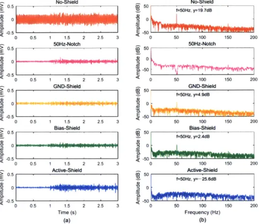
exists several shielding schemes for signal protection as shown in Figure 2-5[22].
CH1 A. No-Shield (Method 1) + CH 3 C. Bias-Shield (Method 3) +H2 B. GND-Shield (Method 2) + CH4 D. Active-Shield (Method 4)
Figure 2-5: Analog signal shielding methods comparison. Reprinted with permission
from [22].
To illustrate Figure 2-5, there exists three primary ways to shield differential
signal cables: GND-shield, bias-shield, and active-shield. In GND-shield case, the
two bipolar signal lines are shielded with the output of an OPAMP driving virtual
ground voltage. This implies that the positive input of the OPAMP is connected
to ground while the output is connected to the negative input. The OPAMP is
driving ground voltage through its output node suppressing external noise to the
ground voltage level. In theory, it is possible to drive shieldings of multiple input
channels with only one OPAMP since they all share the ground node. Bias-shield
and active-shield methods also share the core mechanism. In bias-shield method,
the only difference with GND-shield method is that the OPAMP is driven by bias
generated by the voltage (usually an average of the positive and negative signals of
the diferential pair input). Thus, this bias-shield method requires one OPAMP per
one sEMG input channel. In active-shield method, OPAMP drives each signal line
applying negative feedback canceling out external noises. Figure 2-6 shows a result
of sEMG signal acquisitions with different types of shield methods[221.
>0.5 0 -0.5 0.5 0s 0 0 -0.5 >0.5 0 E-0.5 0.5 V 0 E-0.5 Time (s) (a) No-Shield 0 0.5 1 1.5 2 2.5 3 50Hz-Notch 0 0.5 1 1.5 2 2.5 3 GND-Shield 0 0.5 1 1.5 2 2.5 3 Active-Shield 0 0.5 1 1.5 2 2.5 3 Frequency (Hz) (b)
Figure 2-6:
Result of sEMG measurements with varied of shielding schemes.
Reprinted with permission from [22].
In Figure 2-6, the active-shield method provides the best performance while
bias-shield method and GND-bias-shield method also provide comparable performances. The
efficacies of different shielding methods can be compared objectively in power
spec-trum analysis. In the power specspec-trum analysis of the active-shield method, power
line noise around the frequency of 50 to 60 Hz was not visible. On the contrary,
attenuated power line noise is visible on the power spectrum analyses of GND-shield
method and bias-shield method.
Although the active-shield method provides the best shielding capability, there
exist different criteria to consider. First, the data presented in Figure 2-6 was collected
without twisted-pair signaling from the bipolar electrode. A significant portion of the
noise can be canceled out with the pair cabling scheme. With the
twisted-pair signaling, the effect of using different shield methods might not be as drastic as
50No-Shield 0 0 50 100 150 20( 50Hz-Notch o 5 0 T -50 E < 0 50 100 150 20( GND-Shield f=50Hz, 4.9dB 0 -50 0 50 100 150 20( Bias-Shield 50f=50Hz, y=2A4dB S 0 -50 0 50 100 150 20X Acive-Sheld f=5OHz, y=-25.6dB 0 < 00 50 100 150 204 0
presented in Figure 2-6.
Also, the required resources for each shielding method are largely varied. As discussed above, the active-shield method utilizes two amplifiers per channel, while bias-shield method and GND-shield use one amplifier per channel. In comparison between bias-Shield and GND-shield, the required amount of amplifiers can signifi-cantly different as the number of input channel scales up. Bias-shield method requires reference bias voltage per channel requiring one amplifier per channel. GND-shield method can share one OPAMP on several channel inputs (as many as OPAMP can drive against the noise). Table 2.5 shows the required number of amplifiers for each shielding methods assuming the case of eight-channel sEMG acquisition system.
Table 2.5: Required amplifier resources for different shielding methods. Shielding scheme Required Number of Amplifiers
GND-shield 1
Bias-shield 8
Active-shield 16
Due to a significant difference in the required number of amplifier resources, the designed system implements GND-shield method on the system using the OPAMP
IC , OPA2378 (Texas Instruments).
2.1.5
AFE Design Summary
Based on the discussion made, the AFE was designed based on the following design decisions:
* Use of a miniaturized instrumentation amplifier IC with extremely high input
impedance (Za 2 400M
©
f=100Hz)•
Use of a multi-channel miniaturized ADC with high resolution (ResolutionADC 2 24bit)" Use of low analog gain (< 10)
e Differential twisted signaling with GND-shield
The statements above are the summarized design decisions of the AFE. Based on
the decisions, the overall design of the AFE is depicted in Figure 2-7. Table 2.6 shows
the chosen core components chosen for the AFE.
Body ,,---, Analog-Front-End (AFE)
urface S-CH
notrumnenta on:
Differential Signaling A r
(1WIsted Pair)
+ uV Level
Buffered Signal Low-N
Electro W PWR I HCH -C>H2 SHDI Electrode CH2 CH2 SHD
l High-t solution ADC
I
~~~~
byeartOPMActivei el""din High Input Z
uV Level Signal Input Low Gain
G:510
Electrode Atv~rulN F
CHO
Active Shielding 1A output shielding
-CHO •IA Output
SHD) ,can be driven ... by separate OPAMP Active Shiling Input Signal OPAMP Active Virtual GND Electrode AFE GND AGND) oise nput Digital Signal Output S
Figure 2-7: AFE design summary.
GND
---Table 2.6: Specifications of the selected AFE components.
Component Part Number Manufacturer Note
IA AD8422 Analog Devices Zip = 200GQ || 2pF
ADC ADS1299 Texas Instruments 24-bit, Input referred noise < 1pV
OPAMP OPA2378 Texas Instruments AMPspec
2.2
Design of Power Conditioning Architecture
In embedded system design, proper power conditioning is always a necessary condition to ensure the robustness and the stability of the system. Specifically, in the sEMG application, the role of power conditioning block is significant. Among many roles, some of the critical roles of the power conditioning block are shown in the following:
" Safety of a subject " Power input flexibility
* System robustness
" Efficient power management
The power conditioning block of the constructed sEMG system was designd in order to achieve the roles stated above with minimal footprint. Figure 2-8 shows the abstracted components layout of the power conditioning block of the system, and Figure 2-8 shows the conceptual power flow among these ICs and the functions of them.
Isolated Block TP73525 +2V6 LDO +V +42V, AFE Analog PWR 8-CH A Front E nalog id (AFE) AFE Digital Block +3V3 DigitalR signal
I-WV,
AFE Analog PWRTPS72325 MA889 -2V5 LDOI- -3V3 Inverter) ISOW7842 PWR/COMM Isolator 3V3c 5V + IC filter LMWR16006Y BATT pwR WMe Range SMWPS 9V~ +5V TPS2111
a
'5V PWR MUXr~~I
46v +5V Digital Signal TXBO104 COMM LVSHIFT 5V -> 3V3+sy~
TIPS 73533 3V3 LDO Digital PWR Digital Signal4 Data Flow 4 - PowerFlow
Figure 2-8: Power conditioning block diagram of the hardware. Red blocks represent
selected PMICs.
e ~54 a
5 5 5 3.3 a.S -.3 3.3
5 3.3 3.3 3.3 ..3 -2.5 2.5 StopDown Power Mux LowDropout PWR& COi LC Filter Vot
SMPO Regulao Isolation Inverter LowDropout RWgw PWRguCOUtaoltIlon
Purose High System LOW User LOW High LOW LOW
Efficiency Safety Noise Safety Noise Efficiency Nols Noise
5-4V LMR ---1 V A.V LC TPSv
BATPWR 16006Y TPS ISOW filter
5V
2111 TPS 7842 MAX TPSUSB PW 73533 889 7232
USB PWR 3.3V
3.3V 3.3V -. V 2.5V
Appllailon SytemDigital Blok Isolated AFE Digital Block AFE An lok
Block (U+Vm) BA A AM +ADC
Power High Efficiency
Flow Purpose
Safety Purpose
Low Noise Purpose
Figure 2-9: Power flow diagram among selected PMICs. The purposes of PMICs are
categorized into three groups: high efficiency, safety, and low-noise.
41
Input (V)
output (V)
Generally, each power conditioning IC was chosen with the emphasis of either high efficiency, safety augmentation, or low-noise regulation. As power input flows from an
input voltage source to the functional block (the digital block or the AFE), the supply power to the functional block is converted and regulated efficiently and robustly while ensuring tolerable noise level to each block. Also, the power conditioning block isolates the AFE from the primary power input source and limits maximum power delivery
rates to ensure the safety of a subject. The detailed explanation of Figure 2-8 is discussed in the following subsections.
2.2.1
Safety for Human Subject Trials
The safety of a subject should always be a top priority in biomedical signal acquisition platforms. In general, there exists regulation and guideline for commercial medical devices, IEC-60601[23]. Specifically, electrical isolation and insulation between the main power source and the AFE are the core requirements of the regulation. Although the device was not designed to be commercialized currently, the proposed sEMG system was designed to satisfy the safety regulation requirement.
The physical isolation on the system was established as shown in Figure 2-10. The power and data transmission between the isolated and non-isolated blocks was enabled
with an isolation PMIC, ISOW7842 (Texas Instruments). With the isolator PMIC satisfying the regulation requirement, the safety requirement for patient-acquisition module was satisfied in the design phase.
Eu-U.U
C
-Power Transfer
Analog Front End Block Limit upto 650 mW
SPI Communication
Electrically Isolated 16Mzlo
(a) (b)
Figure 2-10: Isolation scheme of the AFE for a subject safety. (a) 2-Dimensional
multi-plane layout of the electronics hardware emphasizing a physical isolation. (b)
3-Dimensional model of the electronics hardware visualizing the roles of the isolator
PMIC.
2.2.2
Power Input Flexibility
In wearable robotics applications, flexible power input options can be beneficial in
terms of user convenience. Strict power input condition on the electronics requires an
additional embedded system for power regulation that has to be carried by a subject.
As portability is always a requirement in wearable robotics applications, the system
requiring an additional component is not desirable. Thus, the proposed sEMG system
was designed to handle a wide range of power supply conditions. To describe, Figure
2-8 and Figure 2-9 show the power input capability of the sEMG system hardware.
switched-mode-power-supply (SMPS), LMR16006Y (Texas Instruments). This first stage SMPS enables efficient power supply from the power source of voltage range between 9V to 54V and steps down to 5V voltage output. Also, the system was designed to be capable of being powered up by a 5V USB input. This allows the system to be powered directly from a portable single board computer (SBC). Power multiplexer
IC, TPS2111 (Texas Instruments), safely multiplexes the two power sources (main
power source and USB) in order to make sure the system can interface both power sources at the same time. This feature is useful when the system is powered up by a high power battery while the USB communication is required for high-level controller.
2.2.3
System Robustness
As depicted in Figure 2-9, the functional blocks (the digital block or the AFE) receive the power supply from low-noise drop-out regulators. The supply power flows to the functional blocks via cascaded PMICs from high-efficiency PMICs to low-noise regulators. This cascade PMIC approach is effective in designing power flow for insuring robustness of the system while demonstrating reasonable efficiency in power conditioning.
2.3
Design of Digital Processing Backend
2.3.1
Digital Block Requirement
Computational Capability
A main computational processor processes the real-time sEMG post-processing. The
main processor is required to have the hard real-time capability with high data throughput from the AFE to I/O interface for real-time digital signal processing
(DSP). The detailed DSP scheme is discussed in Chapter 3, but bandpass filtering
capability with the frequency of 1kHz is a minimum requirement to process the sEMG signal in order to avoid data aliasing. Also, for hard real-time capability, the digital block requires a hardware clock and a watchdog capability.
Input/Output Interface
The processor is required to have different types of real-time I/0 capabilities for compatibility with different wearable robotics applications. Also, the importance of high communication bandwidth of the I/O interfaces is explicitly emphasized in high-bandwidth closed loop system integration. Although there exist numerous physical communication interfaces for robotics applications, the system aims to provide some of the major interfaces widely used in wearable robotics and mechatronics fields. The selected physical I/0 interfaces of the electronics are shown in the following:
* RS-485
" Inter-Integrated Circuit (12C)
* Serial Periphal Interface (SPI)
" Universal Asynchronous Reciever/Transmitter (UART) " Universal Serial Bus (USB)
Thus, the digital processor of the system was required to have connectivities for the above communication protocols.
Power Consumption and Footprint
Power consumption and footprint size of a computational processor are general trade-offs against computational capability and I/0 versatility. Several computing cores were considered as a main processor such as field-programmable-gate-array (FPGA), microcontroller unit(MCU), and microprocessor. On top of power consumption, real-time capabilities, and computation bandwidth, user interface and ease of reconfiguring and programming are also significantly important for real-world research applications. With qualitative comparison, MCU was chosen as the main processing core. Table
Table 2.7: Comparison of processor tradeoff.
Type Power Real-time Computing Reconfigurability
Consumption Capability Power
FPGA +++ +++ ++ +
MCU ++ +++ ++ +++
Microprocessor ++ + +++ +++
Number of '+' symbols refers to qualitative relative advantages.
2.3.2
Processor Selection
Based on the discussion above, versatile cortex-M4 architecture MCU was selected as a main processor. The chosen MCU part is STM32F405 (ST Microelectronics). Table 2.8 shows brief specifications of the MCU.
Table 2.8: Specifications of the selected MCU.
Specification Value
Part Number STM32F405
Supply Voltage 1.65 ~ 3.6 V (3.3 V is used)
Max Clock Speed 168 MHz
Max Current Consumption 240 mA
Architecture Cortex-M4
I/O Peripherals
GPIO, SPI, I2C, UART, USB, CAN
Flash Memory 1 Mb
Memory Controller Direct Memory Access Enabled
2.4
System Integration
With the considerations and decisions made in this chapter, the embedded system
for sEMG acquisition and processing was designed and manufactured. Figure 2-11
shows the rendered design of the hardware.
(a)
(b)
Figure 2-11: Rendering of the electronics hardware. (a) Top view. (b) Bottom view.
The nominal overall specification of the designed sEMG system is shown in Table
2.9.
Table 2.9: Nominal specifications of the designed sEMG system.
Specification
Value
Size
33 x 60 mm
2Maximum sEMG Sampling Frequency
2 kHZ
Digital Interface
SPI / 12C
/UART
/ RS-485 / USB
PowerInput
USB & 9
54 V voltage source
Number of sEMG Channel
8
Compatibile Electrodes
Ag/AgCl, Dry Metal, Fabric
Dynamic Range
460 mV (±230 mV)
Estimated Noise Level
<
luVrms
User Interface
PWR LED, RGB LED
Figure 2-12 shows the manufactured hardware and the explanation of overall major
lolated Power
Regulation UART I Digital SPi UO ConnectorItC I RS-486
Instrumentation Amplifier EMG Electrode Connector Microcontroller Programmer Microcontroller & Digital 1O USB Connector Main Power Regulation Main Power input
9 -54 V
Active Shielding Driver
ADC
Figure 2-12: Hardware sub-block function summary of the manufactured electronics
hardware.
Table 2.10 shows the core component selections. All the components were selected
from COTS electronics components markets.
Table 2.10: Selected core components of the designed sEMG system.
Block Component
IA1
AFE
ADC
2OPAMP3
Digital Processor Microcontroller Isolator
e
.ation SMPS4USB Power MUX 1. IA: Instrumentatioi Amplifier.
2. ADC: Analog-to-Digital Converter. 3. OPAMP: Operation Amplifier. 4. SMPS: Switched Mode Power Supply.
Part Number AD8422 ADS1299 OPA2376 STM32F405 ISOW7842 LM16006Y TPS2001 Manufacturer Analog Devices Texas Instrument Texas Instrument ST Microelectronics Texas Instrument Texas Instrument Texas Instrument
Detailed design files including schematics and bill of materials are attached in Appendix A and B. As the first prototype, the manufactured system met the required functionality. The detailed evaluation result are discussed in Chapter 4. Also, there exists some design aspects that need to be improved. The required improvements for
Chapter 3
Design of Supporting Softwares
In general, harmonization between hardware and software is necessary to ensure good performance of an embedded system. From the hardware design phase, the designer should consider an overall firmware architecture and evaluate the overall system fea-sibility over time. A firmware and a hardware of the system should be designed complementary to each other. On top of firmware development, interface softwares such as graphic user interface (GUI) or communication interface driver running on a mainframe computer are also required to utilize the electronics hardware properly. These interfaces are critical for users to debug and reconfigure the system in different types of applications. In other words, for successful deployment of the embedded system in real world, the designer of the system should provide a pipeline that users can access the data inside an embedded system through physical byte stream to user-friendly environments such as PC or other measurement equipment.
In this chapter, the design processes of required software stacks for sEMG system are explained in detail. Specifically, the design of software stacks in this thesis refers to the following processes:
" Analysis of requirements for sEMG filtering and post-processing specifically in
wearable robotics applications
" Design and implementation of real-time DSP and post-processing algorithms " Design of the real-time operating system (RTOS) firmware for MCU
* Design of the graphic user interface (GUI) and the communication interface
driver for a mainframe computer
3.1
Real-Time DSP of sEMG Signal
3.1.1
Characteristics of sEMG Signal
Frequency and amplitude characteristics of sEMG signals were well understood in
the field.
124]
notes that bandwidth of sEMG signal generally lies in 20 - 1000 Hz,while
125]
shows that major portion of power spectrum of sEMG signalS lies in the
frequency band under 500 Hz. Figure 3-1 shows a good outline for understanding the
signal characteristics of sEMG signals.
o'10 ECG 10 Uso 102 EMG ° 10° 0C4 00 offset 20-10^' 0.1 Frequency (Hz) 10 100 1000 0 100 200 300 400 So0 Frequency (Hz) (a) (b)
Figure 3-1: General signal characteristics of sEMG signals. (a) Amplitude-Bandwidth
overview of bio-potential signals reprinted with permission from [24]. © Springer Nature. (b) Example sEMG power spectrum analysis reprinted with permission from [25]. © 2019 Delsys Inc.
Also, international standards of sEMG processing for medical purpose recording are shown in Table 3.1.


![Table 2.2: Comparison of measured impedances of varied electrodes. Reprinted with permission from 111]](https://thumb-eu.123doks.com/thumbv2/123doknet/14685719.560206/30.917.265.700.249.391/table-comparison-measured-impedances-varied-electrodes-reprinted-permission.webp)
![Figure 2-5: Analog signal shielding methods comparison. Reprinted with permission from [22].](https://thumb-eu.123doks.com/thumbv2/123doknet/14685719.560206/35.917.175.715.592.918/figure-analog-signal-shielding-methods-comparison-reprinted-permission.webp)


![Figure 3-3: Movement artifact power attenation with passband variation. Reprinted with permission from [28]](https://thumb-eu.123doks.com/thumbv2/123doknet/14685719.560206/56.917.203.691.121.600/figure-movement-artifact-attenation-passband-variation-reprinted-permission.webp)