HAL Id: hal-02986484
https://hal.archives-ouvertes.fr/hal-02986484
Submitted on 21 Dec 2020HAL is a multi-disciplinary open access
archive for the deposit and dissemination of sci-entific research documents, whether they are pub-lished or not. The documents may come from teaching and research institutions in France or abroad, or from public or private research centers.
L’archive ouverte pluridisciplinaire HAL, est destinée au dépôt et à la diffusion de documents scientifiques de niveau recherche, publiés ou non, émanant des établissements d’enseignement et de recherche français ou étrangers, des laboratoires publics ou privés.
Reduced Lasing Thresholds in GeSn Microdisk Cavities
with Defect Management of the Optically Active Region
Anas Elbaz, Riazul Arefin, Emilie Sakat, Binbin Wang, Etienne Herth, Gilles
Patriarche, Antonino Foti, Razvigor Ossikovski, Sebastien Sauvage, Xavier
Checoury, et al.
To cite this version:
Anas Elbaz, Riazul Arefin, Emilie Sakat, Binbin Wang, Etienne Herth, et al.. Reduced Lasing Thresh-olds in GeSn Microdisk Cavities with Defect Management of the Optically Active Region. ACS photonics, American Chemical Society„ 2020, 7 (10), pp.2713-2722. �10.1021/acsphotonics.0c00708�. �hal-02986484�
Reduced lasing thresholds in GeSn microdisk
cavities with defect management of the
optically active region
Anas Elbaz,
†,‡Riazul Arefin,
†Emilie Sakat,
†Binbin Wang,
†Etienne Herth,
†Gilles
Patriarche,
†Antonino Foti,
¶Razvigor Ossikovski,
¶Sebastien Sauvage,
†Xavier
Checoury,
†Konstantinos Pantzas,
†Isabelle Sagnes,
†Jérémie Chrétien,
§Lara
Casiez,
kMathieu Bertrand,
kVincent Calvo,
§Nicolas Pauc,
§Alexei Chelnokov,
kPhilippe Boucaud,
⊥Federic Boeuf,
‡Vincent Reboud,
kJean-Michel Hartmann,
kand Moustafa El Kurdi
∗,††Université Paris-Saclay, CNRS, C2N, 91120, Palaiseau, France ‡STMicroelectronics, Rue Jean Monnet 38054 Crolles, France
¶LPICM, CNRS, Ecole Polytechnique, Université Paris-Saclay, 91120 Palaiseau, France §Univ. Grenoble Alpes, CEA, IRIG-DePhy, 38054 Grenoble, France
kUniv. Grenoble Alpes, CEA, LETI, 38054 Grenoble, France
⊥Université Côte d’Azur, CNRS, CRHEA, Rue Bernard Grégory, CS 10269, 06905 Sophia-Antipolis Cedex France
E-mail: [email protected]
Abstract
GeSn alloys are nowadays considered as the most promising materials to build Group
compatible approach. Recent GeSn laser developments rely on increasing the band structure directness, by increasing the Sn content in thick GeSn layers grown on ger-manium (Ge) virtual substrates (VS) on Si. These lasers nonetheless suffer from a lack of defect management and from high threshold densities. In this work we examine the lasing characteristics of GeSn alloys with Sn contents ranging from 7 % to 10.5 %. The GeSn layers were patterned into suspended microdisk cavities with different diameters in the 4-8 µm range. We evidence direct band gap in GeSn with 7 % of Sn and lasing at 2-2.3 µm wavelength under optical injection with reproducible lasing thresholds around 10 kW cm−2, lower by one order of magnitude as compared to the literature. These results were obtained after the removal of the dense array of misfit dislocations in the active region of the GeSn microdisk cavities. The results offer new perspectives for future designs of GeSn-based laser sources.
Introduction
The weak emission efficiency of group IV materials like Ge and Si can be traced back to their indirect band gap structure. One very promising option to overcome this limit relies on the alloying of Ge with Sn.1,2 Inherently direct band gap materials can indeed be obtained
from GeSn alloys with Sn contents around 7-8 % and above. The material directness can be quantified by the energy splitting, ∆EL−Γ = EL − EΓ, between the indirect L valley
and the direct valley Γ. This energy splitting increases with the Sn content in strain-free GeSn alloys.3,4 This very attractive feature has been the subject of numerous researches, the
aim being to fabricate lasers compatible with group IV elements and complementary metal oxide semiconductor (CMOS) process5–7 which has recently led to an electrically injected
source.8 As the Sn solubility in Ge is limited to only 1 %, i.e. well below the required one
for direct band gap, one has to develop complex metastable growth process for homogeneous incorporation of Sn in Ge. The growth of high quality alloys still remains a challenging task. Growth temperatures below 400°C are mandatory, limiting the crystalline quality and the
ability to cure defects by thermal annealing.9 Moreover, the lattice mismatch between Ge-VS
on Si and GeSn generates compressive strain in the as-grown layers. The compressive strain is known to counteract the effect of Sn incorporation, as it decreases the EL−EΓsplitting energy
and can even invert the band gap alignment.10 One strategy to overcome this compressive
stress while increasing the Sn content in the layer is to reach plastic relaxation. Several approaches were indeed developed to incorporate as much Sn as possible in GeSn alloys to increase their directness while managing the lattice mismatch between the Ge-VS and the epitaxially-grown GeSn layer. With the step graded layer technique,11–13 misfit dislocations
are confined in the lower Sn content layers while high optical quality, high Sn content active layers lie on top. Increasing the Sn content results however in higher density of interface defects, which scales with the lattice mismatch and thus the Sn content.14 Consequently,
a lower crystalline quality is inherent to high Sn content GeSn/Ge growth, which is in turn detrimental to carrier optical recombination dynamics.15 This would explain the very
high pumping levels required to reach population inversion in previously reported high Sn content (>10 %) GeSn lasers although active layers had a direct band gap. One possibility to overcome this limitation is to confine carriers away from interfaces by using SiGeSn barriers in GeSn/SiGeSn double heterostructures or multi-quantum wells (MQW) stackings.16–19 A
reduction of lasing threshold down to 40 kW cm−2,20 as compared with hundreds of kW
cm−2 in bulk layers, was obtained with this approach. However MQWs suffer from rather
small valence band offsets and reduced hole confinement. Their distinct advantages are thus conserved only up to 100 K.20
No works have so far focused to our knowledge on the deleterious impact that defects might have on lasing. To provide some insight about it, we studied relaxed GeSn microdisk cavities with attempts to suppress defects from their active region, specifically the dense array of misfit dislocations at the GeSn/Ge interface. One obvious way is to start with low Sn content layers, with therefore a lower density of misfit dislocations to deal with. In order to investigate the role of band gap directness on the lasing characteristics, once defects were
removed, we explored Sn contents in the 7 % to 10 % range. We thus probed ∆EL−Γ close
to 0 up to 100 meV. We have obtained a drastic reduction of lasing thresholds in GeSn microdisk cavities, as compared to the literature, even for the lowest Sn content sample which had the smallest directness. A specific processing that suppressed interface defects in the active region of the cavity has most likely enabled such improvement. This highlights the key role of defects removal on lasing performances, a strategy which can be used, in the future, in structures with higher Sn contents and therefore higher band gap directness.
Results and discussion
Fabrication
GeSn layers with various Sn contents were grown on Ge-VS on Si (001) substrates. Structural parameters such as residual strain and Sn content were quantified using X-Ray-Diffraction (XRD), Raman spectroscopy and Transmission Electron Microscopy (TEM) (see supporting information). Structural parameters are summarized in Table 1.
Table 1: Structural parameter of the GeSn layers after growth % [Sn] Strain Nominal thickness
7 -0.3 % 500 nm 8.1 -0.37 % 500 nm 10.5 -0.53 % 500 nm
Microdisk cavities were etched into the as-grown layers using the standard processing tools described in the supporting information (SI), with diameters ranging from 4 to 10 µm (Fig. 1-a). Here all microdisks were underetched by typically 1.5 µm from the edges, leaving a very narrow Ge pillar in the central part for disks with a diameter of 4 µm.21 As compared
to other reports,6,22 we used an etching recipe with SF
6 instead of CF4 gas. The latter
yielded a very high selective etching of Ge over GeSn,23 and was thus selected as the best
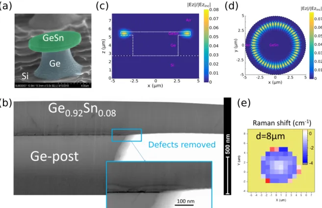
Figure 1: a 3D Scanning Electron Microscopy image of a GeSn microdisk b Bright Field (BF) TEM image of a GeSn microdisk. The lamella was milled by Focused Ion Beam through a microdisk with a 10 µm diameter c Electromagnetic field |Ez|/|Ez−inc| of a TM whispering
gallery mode (L=26, N=1) with an energy of 0.5352 eV in the Oxz plane. d Same as c) in the Oxy plane, the dotted circle shows the edges of the Ge pillar. e 2D map of Raman shift measured on a 8 µm diameter microdisk. The Raman position of TO vibration mode of the as-grown layer is taken as a reference.
chemistry does not enable to etch the bottom defective interface in GeSn as discussed in ref.22 On the other hand, the SF
6 gas is less selective and enables, as discussed in the
following, to remove the defective interface from the active region of the GeSn microdisks. Figure 1-b shows a bright field TEM image of a GeSn microdisk layer with a diameter of 10 µm (more details in the SI). One can see that the as-grown GeSn layer presents a high density of stacking faults and misfit dislocations near the GeSn/Ge interface. Such defects recombine in the first 60 nm by forming dislocation loops parallel to the interface. A lower density of stacking fault segments extend more in depth in the layer with an angle of 54° but without necessarily crossing the whole layer. The Ge etching recipe used to fabricate
the pillar was not infinitely selective over GeSn. This led to a reduced thickness on its bottom side (see SI) as the top surface was protected by the photoresist that defines the pattern. More importantly, the partial etch of the bottom part of the GeSn film resulted in a total removal of the dense misfit dislocation network at the interface. Even in poorly etched areas, i.e. near the Ge pillar, (inset of Fig. 1-b), the layer still had defects removed. Additionally, the stacking fault segments which extended more in depth disappeared from the suspended GeSn area. Both features suggest that additional curing might have occurred in GeSn (see SI). During the Ge etch, the initial GeSn/Ge interface becomes a free GeSn surface which can reconstruct. Curing and enhancement of defect mobility may have been activated by local heating, induced by the plasma etching chemistry. The fact that the GeSn is increasingly suspended in the air during the underetching of Ge minimizes thermal dissipation to the substrate. The current analysis was performed on the sample with an intermediate Sn content of 8 %. Measurements of the GeSn layer thickness at the microdisk edges for Sn contents of 7 % and 10.5 % showed a systematic reduction of this defective region (see SI). One could thus assume that the same defect removal occurred over the whole Sn content range probed in the current work. We emphasize that defects were removed in the most relevant region of the cavity, given that laser emission comes from whispering gallery modes resonances (WGM) (Fig. 1-c-d). The suppression of dislocations in the outer-parts of the GeSn microdisk should have a positive impact on carrier recombination dynamics, optical losses, and thus on material gain and threshold.
A first analysis by Raman spectroscopy of microdisk strain showed that strain relaxation occurred in suspended parts of the layer. Figure 1-e is a 2D-surface map of Raman shift measured using the Raman spectral position of the as-grown layer as a reference. The central area of the microdisk above the Ge pillar has quasi-unrelaxed strain, here for a microdisk with a 8 µm diameter. Strain relaxation, characterized by a Raman red-shift, occurs in the suspended part of the layer, which has an optimized overlap with WGMs. The relaxation of compressive strain enables to increase the band gap directness parameter and promote
optical gain10,22 in this defect-free region. Further Raman analysis was performed on the
microdisks to assess the strain relaxation in small microdisk diameters of around 4 µm, as studied in photoluminescence (PL). A homogeneous strain distribution along the diameter was obtained in those cases (see SI).
Optical analysis
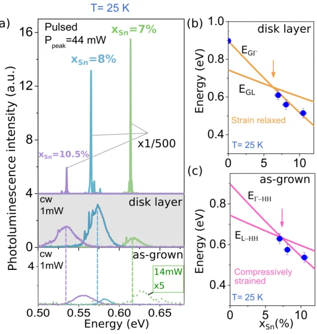
The PL analysis of GeSn layers with various Sn contents was performed at 25 K under 1550 nm wavelength optical pumping. Spectra are shown in Figure 2-a as follows : bottom: PL spectra under continuous wave (cw) pumping on as-grown layers, middle: after patterning of the layers into small 4 µm diameter microdisks under cw excitation, and top: under 3.5 ns duration pulsed excitation with a 25 MHz repetition rate. As discussed below, the combination of 7 % of Sn with 0.3 % of compressive strain should result in an indirect band gap alignment of the band structure. As shown in Figure 2-a bottom, the layer with 7 % Sn exhibits a much lower PL signal as compared to the other samples with higher Sn contents. The signal was indeed too low to be detected under 1 mW excitation power. We thus had to increase the excitation power up to 14 mW and multiply the obtained signal intensity by a factor of 5 to compare its amplitude with the signals for xSn = 8% and 10.5 % under 1 mW
Figure 2: a-bottom, PL spectra from as-grown GeSn layers under 1 mW cw pump power (0.9 kW cm−2 power density), except for the x
Sn = 7% layer pumped with a 14 mW pump
power (12 kW cm−2 power density) and a signal multiplied by a factor of 5. Middle, PL
spectra from layers patterned into 4 µm diameter microdisks, under cw excitation of 1 mW. Top, same as middle but excitation is turned into a pulsed mode with a 44 mW peak power, (38 kW cm−2 power density). Spectra has been offset and divided by a factor of 500. b
Experimental values of fundamental band gap obtained from PL spectra under cw pumping of microdisks. Orange lines correspond to modeled direct and indirect band gap energies EGΓ and EGL of relaxed GeSn layers with bowing parameters bL = 0.89 eV and bΓ = 2.77
eV. The arrow shows the indirect-direct bandgap crossover. c same as (b) but for as-grown layers assuming 30 % of residual compressive strain due to the lattice parameter mismatch (between GeSn and Ge).
After patterning the layers into microdisks, we observed clear red-shifts in PL spectra due to the full relaxation of the residual compressive stress by underetching. Note that the spectra from 4 µm diameter microdisks are shown in Figure 2-a using the same scale as for PL spectra on as-grown layers to facilitate comparison.
The band gaps were extracted from the PL spectra under cw excitation. They are plotted in Figures 2-b and -c for respectively the microdisks and as-grown layers. In the same figure, we have plotted the theoretical band gap of GeSn alloys assuming 30 % (see SI) of residual compressive strain for the as-grown layers (Figure 2-c). Meanwhile, the strain is assumed to be completely relaxed in microdisks with very narrow Ge pedestals (Figure 2-b) as evidenced by Raman spectroscopy (see the SI). The experimental energy dependencies on Sn content are properly fitted with an empirical quadratic law EΓ,L(xSn) =
EGe
Γ,L× (1 − xSn) + EΓ,LSn × xSn− bΓ,L(1 − xSn)xSn. The following valley energies were fixed:
EΓSn = −0.408 eV and ELSn = 0.12 eV, EΓGe = 0.898 eV, ELGe = 0.744 eV while bL = 0.89
eV according to ref.24 As we have achieved lasing for microdisks with Sn contents above
7 %, we therefore assume that the microdisk emission stems from direct transitions. The experimental band gap dependence on Sn content shown in Figure 2-b was thus fitted with EΓ(xSn) by adjusting the bowing parameter and adopting bΓ = 2.77 eV, a value close to
the 2.46 eV energy reported in ref.25 In previous reports, for instance in ref.,24,26 where
bΓ = 2.24 eV and bL = 0.89 eV were used, the indirect-direct band gap crossover was
expected to occur at around 8 % of Sn, as also reported in ref.1,4,27–29 Here, it occurred at
6.4 %, in good agreement with the modeled one for relaxed GeSn alloys.30 In ref.,27,29 a
composition-dependent law was proposed: bΓ = 2.66 − 0.54xSn, e.g. around 2.61 eV for the
7-10% Sn content range considered here and in satisfying agreement with the 2.77 eV value that we found, even if it remains lower. In ref.,27,29 the crossover is however found also for
an higher Sn content, e.g. 8%, than in this work. The differences in crossover values may stem from the presence of residual compressive strain in the layers used to determine it and from a higher value for bL, in the range of 1 eV in ref.27,29 Here the crossover value comes
from fits of data on suspended, strain-free layers. The value of 0.89 eV for bL is consistent
with our experimental results, i.e. that the relaxed layer with 7% Sn content has a direct band gap at 25 K and an indirect band gap when compressively strained by 0.3%.
The latter bowing parameters were subsequently used to calculate the band gap of as-grown layers (see SI), taking into account the impact of residual compressive strain on the band structure (30 % of the residual strain due to lattice parameter mismatch for all Sn contents). Since the compressive strain lifts the degeneracy of the valence band with the heavy-hole (HH) band being the highest in energy, we calculate the direct EΓ−HHand indirect
EL−HH gap energies and compare them with data from as-grown layers (Figure 2-c). Figure
2-c indicates that the combination of 7 % of Sn with 0.3 % of compressive strain should result in an indirect band gap alignment.
We have observed, for all Sn contents, an enhancement of the PL emission for patterned, relaxed, layers as compared to still compressively-strained as-grown ones as seen in Figure 2-a middle. The enhancement depends on the Sn content (enhancement factors of 1.5 and 5 for 10.5 % and 8 % of Sn to be compared with two orders of magnitude for 7 % of Sn). Several factors can explain the microdisk PL amplitude change as compared to as-grown layers : i) obviously, improved radiative efficiency because of defect removal from the bottom of GeSn layers ii) the change of radiation pattern of the overall emission in patterned layers, and iii) the increase of the band structure directness, favoring an electron population in the Γ valley after optical excitation. Carriers in the Γ valley have a higher radiative recombination rate at zone center, i.e. a higher PL efficiency, while carriers in the L valley do not contribute significantly to the PL signal.
For the GeSn layer with xSn = 7 %, the PL enhancement is very strong since the band
gap changes from indirect to direct. We estimate ∆EL−Γ to be −8 meV in the as-grown layer,
i.e. the quasi-totality of electrons are in the L-valley at low temperature and thus the PL signal stems from weak indirect transitions. Meanwhile, ∆EL−Γ = 16meV in the strain-free
direct transitions to the PL signal. A clear signature of direct band alignment in the strain-free sample with xSn = 7 % is the observation of lasing when the microdisk is optically
pumped at higher powers using pulsed excitation (Figure 2-a - see discussion in the next paragraph).
For the xSn = 8 % sample, the ∆EL−Γ splitting energy increases from 11 meV up to
39 meV resulting as well in a significant increase of the NΓ population. The change of
directness for this sample also explains the higher PL amplitude.
For the xSn = 10.5% sample, the directness is expected to change from 51 meV in the
as-grown layer with residual compressive strain to 94 meV in the strain-relaxed microdisk. The low temperature electron population NΓ in the Γ valley is expected to be equivalent
in both cases. The directness increase is thus not the parameter explaining the PL signal enhancement at low temperature. It is rather, in this case, the scattering of emitted light at the microdisk edges and the interface defect removal that predominate. Note that electro-magnetic simulation (with Fourier-Bessel modal method)31 show a lower light absorption in
the GeSn microdisks, by a factor of 0.8, as compared to as-grown layers during the optical pumping. While the microresonator absorbs light more efficiently, the smaller illuminated volume of the microdisk (with 4 µm diameter only, while the excitation spot size was 12 µm) limits the radiative recombination rate.
Low temperature lasing
Low temperature, at 25 K, PL measurements were performed, for each Sn content, on 4 µm diameter microdisks. The power dependence and the measured PL spectra as well as the integrated intensity (L-L) curves are shown in Figure 3. These measurements were performed in a pulsed excitation regime with a 1.55 µm wavelength laser, with 3.5 ns long pulses and a repetition rate of 25 MHz. The laser beam was focused into a 12 µm diameter spot on the sample surface. Under these conditions, the pump power density can be obtained by multiplying the incident power on the sample surface by a 0.88 × 106cm−2 factor. For
all samples, we reached a laser emission regime, characterized by an abrupt transition from broad and weak to intense and narrow emission lines at a well-defined pump power threshold. Above threshold, as typically shown in the inset of Figure 3 for the 8 % sample, a single lasing mode dominates the spontaneous emission background by typically 3 orders of magnitude. Furthermore, the linewidth of the laser mode is typically in the 100 µeV range against meV in previously reported GeSn lasers. We emphasize that this small linewidth can be observed here thanks to the experimental conditions and the low lasing threshold. Indeed, high photon flux yielded by high duty cycle excitation enables high-resolution analysis down to 60 µeV. In previous studies, the very high lasing thresholds required the use of low optical pumping duty cycles in the 10−5 to 10−2 range, to reach the requested very high pump power
densities while avoiding sample heating and damaging. In the present work, the lower lasing thresholds enabled us to use only 10−1 of duty cycle and thus a higher photon flux without
Figure 3: (Bottom) Pulsed peak power dependence of emission spectra for 4 µm diameter microdisks with Sn contents between 7 % to 10.5 % with corresponding L-L curves at 25 K (Top). The continuous curves in the figures on top are calculated curves using the laser rate equations with the indicated thresholds and beta factors. The insets show typical spectra above lasing threshold.
The L-L curves for all microdisks show an S-shape and can be fitted using the laser rate equations given in ref.32 We extracted from the L-L curves the thresholds and the
spontaneous emission beta factors, as given in the inset. The beta factors were obtained by integrating the whole emission spectrum to enable comparison with previous reports on GeSn microdisk lasers.6,7,22 This strategy differs from the standard approach where only the
power in the lasing mode is considered to plot the L-L curves. Beta factors, around 2 %, were uncorrelated with the Sn content. Such a value is much higher than values usually measured for microdisk cavities in the literature.33 We emphasize that when the emission is collected
the laser dynamics.34Only a small fraction, of typically a few % of the WGMs which radiate
preferentially along the disk plane, is collected by the objective. Moreover the spontaneous emission, which is preferentially collected from the top surface since it radiates vertically, has a much broader spectral distribution than the WGM lasing mode.
The thresholds were determined as 17.6 kW cm−2, 8 kW cm−2 and 19 kW cm−2 for
mi-crodisks with 7 %, 8 % and 10.5 % of Sn. Those thresholds are in the 10 kW cm−2 range, to
be compared with previous thresholds in higher Sn content lasers, typically a few hundreds of kW cm−2. More specifically, the lasing threshold for the GeSn 8 % is much lower than those
in previous reports,22,35 i.e. 130 kW cm−2 for a microdisk with an equivalent Sn content.
These values are also lower than those obtained in a specifically-designed multi-quantum well structure (40 kW cm−2) that should in principle have a reduced threshold, through the
quantization of electronic state energies, and separation of optically active media away from the defective regions.20
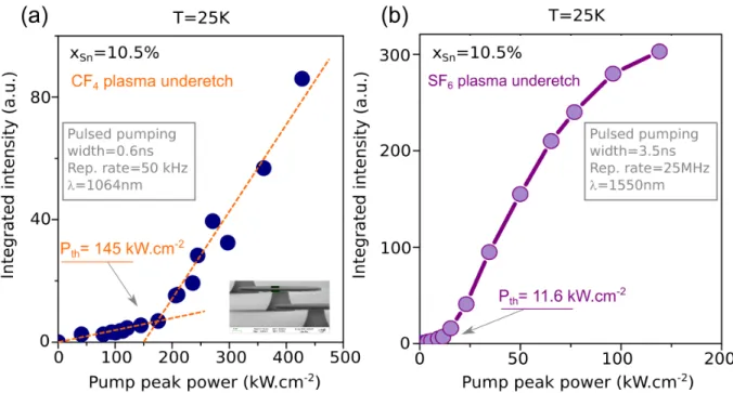
The use of SF6 gas for the microdisk underetching is a key asset to reach such low
thresholds. Figure 4 shows the lasing characteristics of a microdisk fabricated with the same sample with 10.5 % of Sn but using CF4 as underetching gas. The threshold is around
145 kW cm−2, i.e. in the same range as mentioned above from literature data. Such high
excitation range required to change the optical pumping scheme to avoid sample heating and damaging. Shorter pulse duration (0.6 ns) and lower repetition rate (50 kHz) were used as indicated on figure 4-a. As a comparison, we show the lasing characteristics (more data in the SI) of a microdisk of an equivalent size underetched by the SF6 plasma. In this case
the lasing threshold is around 11.6 kW cm−2. This indicates the prominent role played by
microdisk processing on the laser performances, beyond the arguments on Sn content and band structure directness. Starting from the same active region, a reduction by more than one order of magnitude of the threshold can be obtained with an appropriate processing. The removal of the dense array of defects from the active region is obviously one key feature.
Figure 4: a L-L curve obtained at 25 K from a 10 µm diameter microdisk with 10.5 % of Sn underetched with a CF4 plasma. The dashed lines are drawn to guide the eyes. The inset
shows a SEM image of such microdisks b L-L curve obtained at 25 K from a 8 µm diameter microdisk fabricated from the same epitaxial layer with 10.5 % of Sn but underetched with a SF6 plasma.
Temperature dependence
We have studied the lasing temperature dependence for different Sn content microdisks to understand the influence of band gap directness on maximum lasing temperature. The L-L curves measured for various Sn content microdisks and different temperatures are plotted in Figure 5-a. The emission spectra obtained with pump powers above thresholds are shown in Figure 5-b. Additional measurements with 5 K temperature steps (presented in the SI) show that the sample with 7 % of Sn can even support lasing at temperatures up to 80-85 K, like samples with Sn contents of 8 % and 10.5 % which support lasing up to 85-95 K. The general trend in the literature is that higher Sn contents result in higher maximum lasing temperature. The main reason is a reduction of the carrier scattering rate from to Γ to L valleys due to an increase of the energy barrier ∆EL−Γ, enabling an efficient injection of
Figure 5: a L-L curves at temperatures from 25 K to 105 K, for GeSn microdisks with a 4 µm diameter and Sn contents xSnof 7 %, 8.1 % and 10.5 %. No lasing is observed at temperatures
above 100 K. b Emission spectra above lasing threshold for temperatures varying from 25 K to 105 K.c Integrated PL signal from microdisks with different Sn contents as a function of temperature measured under cw excitation below lasing threshold.d Calculated electron population ratio in the Γ valley as a function of temperature for different conduction band barrier energies ∆E = E −E .e Maximal lasing temperature as a function of investigated
In our experiment, we observe very similar maximum lasing temperatures for microdisks, with a maximum temperature increase of only 10-15 K for Sn contents between 7 % and 10.5 %, while ∆EL−Γ = EL− EΓ is expected to vary significantly, from 16 meV for 7 % of Sn
up to 94 meV for 10.5 % of Sn (Figure 5-e). Since the quenching of lasing with increasing temperature can be related to the quenching of population in the Γ valley, we have studied the microdisk PL below threshold under cw pumping as a function of temperature. The PL signal is sharply quenched at temperature above 100 K in a similar way for the various Sn content microdisks (Figure 5-c). Experimentally, the quenching of PL signal is therefore independent of ∆EL−Γ. To better quantify the thermal activation of Γ-L scattering, we have
calculated the equilibrium electron population ratio NΓ
(NΓ+NL) as a function of temperature
for several values of the splitting energy between both bands ∆EL−Γ. Figure 5-d shows the
predicted electron distribution rate in the Γ valley as a function of temperature for different ∆EL−Γ from 0 up to 200 meV and fixed total carrier density (NΓ+ NL) of 1018 cm−3. The
Γ-valley population varies slowly with temperature and does not show a quenching as sharp as the one observed in PL signal. It is thus reasonable to suppose that other parameters influence the maximum lasing temperature beside band structure parameters.
Most probably, the abrupt quenching of lasing and PL for all Sn contents investigated here can be associated with the activation of non-radiative processes as the temperature increases. Above 100 K, non-radiative processes dominate the radiative process and prevent lasing. A systematic study has recently evidenced the presence of vacancy defects in as-grown layers with Sn contents from 6 % to 13 %, corresponding to the range probed here.36 These
defects might be due to the low temperature required to grow metastable GeSn layers above the Sn solubility limit. Vacancies result in a p-type doping of the layers, and thus in optical losses when activated by a temperature increase. Additionally, p-type defects are usually known to shorten coherence lifetimes due to valley scattering. It increases the homogeneous broadening of oscillator strength and the optical gain is therefore weakened.37
Discussion
Microdisks with different diameters and pillar diameters were investigated as well (See SI). For microdisks with an undercut of 1.5 µm, we have obtained reproducible lasing threshold values for diameters of 4-5 µm (See SI), 17.6 kW cm−2 for x
Sn = 7%, 8 kW cm−2 for xSn =
8% and 8.9 kW cm−2 for xSn = 10.5%. The thresholds were reduced when the Sn content
increased from xSn = 7%to xSn = 8%and remained quasi-unchanged for higher Sn contents.
The decrease of the lasing threshold when increasing the Sn content is similar to the one modeled for the carrier density threshold to obtain transparency as a function of ∆EL−Γ, as
Figure 6: a Carrier density threshold to reach transparency as a function of the directness parameter ∆EL−Γ at 20 K in strain-free material. The black circles show the corresponding
relaxed GeSn microdisks with the Sn contents probed in this work b Review of low tem-perature lasing thresholds in GeSn devices as a function of the Sn content in the active media (FP stands for Fabry-Perot). We show only threshold below 25 K. Relaxed GeSn disk cavities are shown as blue circles,6,7,22 while results obtained with compressive GeSn ridge
waveguides appear as pink diamonds,1,35,38 including complex multilayers. More data and
details on experimental conditions used for previous works can be found in the comparison table reported in ref.5 Black, grey and light blue squares are current values. The dashed line
is drawn to show the trend.
The method used for the calculation is detailed in ref.37,39,40 On this figure we can see
that, at low temperature, the carrier density threshold to reach transparency decreases very rapidly at the indirect-direct crossover and stabilizes typically for ∆EL−Γ above 30 meV, i.e.
for xSn above 8 %. Here, the modeling predicts a threshold reduction by typically a factor
2 from xSn = 7% to xSn = 8%, which can instructively be compared with the threshold
reduction observed experimentally for these layers, from 17.6 kW cm−2 for x
Sn = 7% down
to 8 kW cm−2 for x
with different cavity designs, showed a very wide range of thresholds.
We note that the measured thresholds can depend on many factors, like the microdisk thickness, the pillar sizes, the laser cavity geometries as well as the excitation conditions (pump wavelength, duty cycle, and repetition rate). The data shown on Figure 6-b use the comparison data reported in ref.5 with a very wide range of pumping conditions and cavity
designs, which are recalled on figure 6-b were considered. In this work, the thicknesses are very similar to those reported in ref.5 The optical pumping conditions are also similar, only
the duty cycle is much higher here. Note that it is not favorable, since as discussed in the SI, a higher duty cycle induces heating of the gain media as compared the low duty cycle used in previous reports. All reported thresholds are given in terms of peak power densities which govern the injected carrier densities, independently of the duty cycle. Our measurements suggest that there is no clear threshold dependence on Sn contents above 8 %, i.e. on band structure directness. We suggest that the limiting factors previously reported were not band structure issues,1,6,7,13,22,35,38but material and processing issues, that have been partly solved
here thanks to the removal of the defective GeSn/Ge interface. We recall that the lasing threshold depends on the carrier density needed to reach transparency, i.e. directly dependent on the density of states, the cavity characteristics implying the dynamic gain and quality factor, and the radiative and non-radiative lifetimes. From our modeling of carrier density thresholds and measured lasing power density thresholds, one can extract an effective carrier lifetime following the generation-recombination balance law N = Iτ/(hνd), where I is the absorbed power density, τ the recombination lifetime, hν the energy of absorbed photon. d is the layer thickness where the generated carrier density N is distributed. The incident power is multiplied by 0.65 to account for the microdisk surface reflectivity at 1550 nm wavelength. A pumping power of typically 10 kW cm−2is found necessary to reach lasing. One can assume
that lasing in the microdisks cavities can be reached for carrier densities of roughly 4 times the transparency thresholds.40 This corresponds to an injected carrier density of typically
for carrier densities of typically 4 × 1017cm−3. The extracted value for τ is then around 1.3
ns. This value is found in good agreement with the one obtained in a previous report,40where
the microdisk layers were made free from the interface defects, after they were transferred on a host Si-substrate. We postulate that the significant reduction in threshold observed in this work is associated with an increased carrier lifetime, as a consequence of the interface defects removal. In ref.,40 it was shown that a bonding procedure can lead to a GeSnOI stack. In
this approach, one can subsequently remove the defects entirely close to the surface, over the whole wafer area, by simply etching it and obtain layers free from the interface defects like in the present work. In this configuration, one can design various defect-free laser cavities, like Fabry Perot ridge, since there is no need to make additional underetching to remove the defects.
We have reached a maximum lasing temperature of around 95 K with Sn contents lower than or equal to 10.5 %. Higher maximum lasing temperatures were reached with higher Sn content layers and therefore higher band gap directness.6,38 We however found that the
maximum lasing temperature depended very weakly on the Sn content, at least in the range probed here, and thus on band gap directness.
We emphasize that an increased directness can also be obtained by applying tensile strain to the alloys instead of increasing their Sn content. These past years, several methods were indeed developed with the aim to change pure Ge into a direct band gap semiconductor and reach lasing with it.41–43 For Ge, 1.7 % of biaxial tensile strain,44,45 and 4.9 % uniaxial
tensile strain were achieved. These methods could be used on GeSn alloys46 in order to
increase their directness, notably for the reduced Sn contents probed here. Tensile strain even presents the advantage, over the increase of Sn content, of lifting the valence band degeneracy and thus reducing the density of states yielding lower gain threshold than in relaxed GeSn.24,40,47
Conclusion
Low Sn content GeSn layers were used, despite their small band gap directness, to fabricate suspended microdisks exhibiting significantly reduced lasing thresholds as compared to pre-vious reports in the literature. We used a specific processing step that led to the removal of the array of misfit dislocations at the GeSn/Ge interface in the active suspended area of the microdisk cavities. This was most likely the reason why we had a lasing threshold reduction by one order of magnitude as compared to the literature. We were able to con-firm the influence of the band gap directness on lasing thresholds. Higher thresholds were obtained in microdisks with 7 % of Sn, i.e. a lower band gap directness of only few meV as compared to samples with Sn contents of 8 % and higher. We also found that in the explored range of 7 %-10.5 % range, the maximum lasing temperature depended only weakly on Sn content. Our results indicate that, beyond band gap directness, getting rid of non-radiative recombinations, including point defects, is mandatory to reach high temperature lasing.
Acknowledgement
E. Sakat and M. El Kurdi thank J.-P. Hugonin for fruitful discussions on electromagnetic simulations. This work was supported by the French RENATECH network, the French National Research Agency (Agence Nationale de la Recherche, ANR) through funding of the ELEGANTE project (ANR-17-CE24-0015). A. Elbaz was supported by ANRT through a CIFRE grant. Antonino Foti acknowledges funding within the ANR-16-CE09-0029-03 TIPTOP project.
Supporting Information Available
Supplementary information file is available free of charge at http://pubs.acs.org. List of content : Material growth and characterization, Fabrication, Additional data with different
microdisks sizes
References
(1) Wirths, S.; Geiger, R.; Driesch, N. v. d.; Mussler, G.; Stoica, T.; Mantl, S.; Ikonic, Z.; Luysberg, M.; Chiussi, S.; Hartmann, J. M.; Sigg, H.; Faist, J.; Buca, D.; Grütz-macher, D. Lasing in direct-bandgap GeSn alloy grown on Si. Nature Photonics 2015, 9, 88–92.
(2) Soref, R. A.; Buca, D.; Yu, S.-Q. Group IV Photonics - Driving Integrated Optoelec-tronics. Optics & Photonics News 2016, 27, 32–39.
(3) Chen, R.; Lin, H.; Huo, Y.; Hitzman, C.; Kamins, T. I.; Harris, J. S. Increased photolu-minescence of strain-reduced, high-Sn composition Ge1-xSnx alloys grown by molecular beam epitaxy. Applied Physics Letters 2011, 99, 181125.
(4) Grzybowski, G.; Beeler, R. T.; Jiang, L.; Smith, D. J.; Kouvetakis, J.; Menéndez, J. Next generation of Ge1-ySny (y = 0.01-0.09) alloys grown on Si(100) via Ge3H8 and SnD4: Reaction kinetics and tunable emission. Applied Physics Letters 2012, 101, 072105.
(5) Du, W.; Thai, Q. M.; Chrétien, J.; Bertrand, M.; Casiez, L.; Zhou, Y.; Margetis, J.; Pauc, N.; Chelnokov, A.; Reboud, V.; Calvo, V.; Tolle, J.; Li, B.; Yu, S.-Q. Study of Si-Based GeSn Optically Pumped Lasers With Micro-Disk and Ridge Waveguide Structures. Frontiers in Physics 2019, 7, 147.
(6) Reboud, V. et al. Optically pumped GeSn micro-disks with 16% Sn lasing at 3.1 µm up to 180 K. Appl. Phys. Lett. 2017, 111, 092101.
Hartmann, J.-M.; Reboud, V.; Calvo, V. GeSn heterostructure micro-disk laser oper-ating at 230K. Opt. Express 2018, 26, 32500–32508.
(8) Zhou, Y. et al. Electrically injected GeSn lasers on Si operating up to 100K. Optica 2020, 7, 924–928.
(9) Zaumseil, P.; Hou, Y.; Schubert, M. A.; von den Driesch, N.; Stange, D.; Rainko, D.; Virgilio, M.; Buca, D.; Capellini, G. The thermal stability of epitaxial GeSn layers. APL Materials 2018, 6, 076108.
(10) Gupta, S.; Magyari-Köpe, B.; Nishi, Y.; Saraswat, K. C. Achieving direct band gap in germanium through integration of Sn alloying and external strain. Journal of Applied Physics 2013, 113, 073707.
(11) Aubin, J.; Hartmann, J.-M.; Gassenq, A.; Rouviere, J. L.; Robin, E.; Delaye, V.; Cooper, D.; Mollard, N.; Reboud, V.; Calvo, V. Growth and structural properties of step-graded, high Sn content GeSn layers on Ge. Semiconductor Science and Technology 2017, 32, 094006.
(12) Dou, W.; Benamara, M.; Mosleh, A.; Margetis, J.; Grant, P.; Zhou, Y.; Al-Kabi, S.; Du, W.; Tolle, J.; Li, B.; Mortazavi, M.; Yu, S.-Q. Investigation of GeSn Strain Re-laxation and Spontaneous Composition Gradient for Low-Defect and High-Sn Alloy Growth. Scientific Reports 2018, 8, 5640.
(13) Dou, W.; Zhou, Y.; Margetis, J.; Ghetmiri, S. A.; Al-Kabi, S.; Du, W.; Liu, J.; Sun, G.; Soref, R. A.; Tolle, J.; Li, B.; Mortazavi, M.; Yu, S.-Q. Optically pumped lasing at 3 µm from compositionally graded GeSn with tin up to 22.3%. Optics Letters 2018, 43, 4558.
(14) Gencarelli, F.; Vincent, B.; Demeulemeester, J.; Vantomme, A.; Moussa, A.; Fran-quet, A.; Kumar, A.; Bender, H.; Meersschaut, J.; Vandervorst, W.; Loo, R.;
Cay-max, M.; Temst, K.; Heyns, M. Crystalline Properties and Strain Relaxation Mecha-nism of CVD Grown GeSn. ECS Transactions 2013, 50, 875–883.
(15) Pezzoli, F.; Giorgioni, A.; Patchett, D.; Myronov, M. Temperature-Dependent Photo-luminescence Characteristics of GeSn Epitaxial Layers. ACS Photonics 2016, 3, 2004– 2009.
(16) von den Driesch, N.; Stange, D.; Rainko, D.; Povstugar, I.; Zaumseil, P.; Capellini, G.; Schröder, T.; Denneulin, T.; Ikonić, Z.; Hartmann, J.-M.; Sigg, H.; Mantl, S.; Grütz-macher, D.; Buca, D. Advanced GeSn/SiGeSn Group IV Heterostructure Lasers. Advanced Science 2018, 5, 1700955.
(17) Stange, D.; von den Driesch, N.; Rainko, D.; Roesgaard, S.; Povstugar, I.; Hartmann, J.-M.; Stoica, T.; Ikonic, Z.; Mantl, S.; Grützmacher, D.; Buca, D. Short-wave infrared LEDs from GeSn/SiGeSn multiple quantum wells. Optica 2017, 4, 185–188.
(18) von den Driesch, N.; Stange, D.; Wirths, S.; Rainko, D.; Povstugar, I.; Savenko, A.; Breuer, U.; Geiger, R.; Sigg, H.; Ikonic, Z.; Hartmann, J.-M.; Grützmacher, D.; Mantl, S.; Buca, D. SiGeSn Ternaries for Efficient Group IV Heterostructure Light Emitters. Small 2017, 13, 1603321.
(19) Du, W.; Ghetmiri, S. A.; Margetis, J.; Al-Kabi, S.; Zhou, Y.; Liu, J.; Sun, G.; Soref, R. A.; Tolle, J.; Li, B.; Mortazavi, M.; Yu, S.-Q. Investigation of optical tran-sitions in a SiGeSn/GeSn/SiGeSn single quantum well structure. Journal of Applied Physics 2017, 122, 123102.
(20) Stange, D.; von den Driesch, N.; Zabel, T.; Armand-Pilon, F.; Rainko, D.; Marzban, B.; Zaumseil, P.; Hartmann, J.-M.; Ikonic, Z.; Capellini, G.; Mantl, S.; Sigg, H.; Witzens, J.; Grützmacher, D.; Buca, D. GeSn/SiGeSn Heterostructure and Multi Quantum Well Lasers. ACS Photonics 2018, 5, 4628–4636.
(21) Herth, E.; Baranski, M.; Berlharet, D.; Edmond, S.; Bouville, D.; Calvet, L. E.; Gorecki, C. Fast ultra-deep silicon cavities: Toward isotropically etched spherical sili-con molds using an ICP-DRIE. Journal of Vacuum Science & Technology B 2019, 37, 021206.
(22) Stange, D. et al. Optically Pumped GeSn Microdisk Lasers on Si. ACS Photonics 2016, 3, 1279–1285.
(23) Gupta, S.; Chen, R.; Huang, Y.-C.; Kim, Y.; Sanchez, E.; Harris, J. S.; Saraswat, K. C. Highly Selective Dry Etching of Germanium over Germanium-Tin (Ge1-xSnx): A Novel Route for Ge1-xSnx Nanostructure Fabrication. Nano Letters 2013, 13, 3783–3790. (24) Rainko, D.; Ikonic, Z.; Elbaz, A.; von den Driesch, N.; Stange, D.; Herth, E.;
Bou-caud, P.; El Kurdi, M.; Grützmacher, D.; Buca, D. Impact of tensile strain on low Sn content GeSn lasing. Scientific Reports 2019, 9, 259.
(25) Bertrand, M.; Thai, Q.-M.; Chrétien, J.; Pauc, N.; Aubin, J.; Milord, L.; Gassenq, A.; Hartmann, J.-M.; Chelnokov, A.; Calvo, V.; Reboud, V. Experimental Calibration of Sn-Related Varshni Parameters for High Sn Content GeSn Layers. Annalen der Physik 2019, 531, 1800396.
(26) Rainko, D.; Ikonic, Z.; Vukmirović, N.; Stange, D.; von den Driesch, N.; Grütz-macher, D.; Buca, D. Investigation of carrier confinement in direct bandgap GeSn/SiGeSn 2D and 0D heterostructures. Scientific Reports 2018, 8, 15557.
(27) Gallagher, J. D.; Senaratne, C. L.; Kouvetakis, J.; Menéndez, J. Compositional de-pendence of the bowing parameter for the direct and indirect band gaps in Ge1-ySny alloys. Applied Physics Letters 2014, 105, 142102.
(28) Senaratne, C. L.; Gallagher, J. D.; Jiang, L.; Aoki, T.; Smith, D. J.; Menéndez, J.; Kou-vetakis, J. Ge1-ySny (y = 0.01-0.10) alloys on Ge-buffered Si: Synthesis, microstructure,
(29) Menéndez, J.; Wallace, P. M.; Xu, C.; Senaratne, C. L.; Gallagher, J. D.; Kouvetakis, J. Materials physics of GeSn-based semiconductor lasers. Materials Today: Proceedings 2019, 14, 38 – 42.
(30) Dutt, B.; Lin, H.; Sukhdeo, D. S.; Vulovic, B. M.; Gupta, D., S.and Nam; Saraswat, K. C.; Harris Jr., J. S. Theoretical Analysis of GeSn Alloys as a Gain Medium for a Si-Compatible Laser. IEEE Journal of Selected Topics in Quantum Electronics 2013, 19, 1502706–1502706.
(31) Bonod, N.; Popov, E.; Nevière, M. Differential theory of diffraction by finite cylindrical objects. J. Opt. Soc. Am. A 2005, 22, 481–490.
(32) Rosencher, E.; Vinter, B. In Optoelectronics; Piva, P. G., Ed.; Cambridge University Press, 2002.
(33) Sellés, J.; Brimont, C.; Cassabois, G.; Valvin, P.; Guillet, T.; Roland, I.; Zeng, Y.; Checoury, X.; Boucaud, P.; Mexis, M.; Semond, F.; Gayral, B. Deep-UV nitride-on-silicon microdisk lasers. Scientific Reports 2016, 6, 21650.
(34) Mohideen, U.; Hobson, W. S.; Pearton, S. J.; Ren, F.; Slusher, R. E. GaAs/AlGaAs microdisk lasers. Applied Physics Letters 1994, 64, 1911–1913.
(35) Al-Kabi, S. et al. An optically pumped 2.5 µm GeSn laser on Si operating at 110K. Applied Physics Letters 2016, 109, 171105.
(36) Assali, S.; Elsayed, M.; Nicolas, J.; Liedke, M. O.; Wagner, A.; Butterling, M.; Krause-Rehberg, R.; Moutanabbir, O. Vacancy complexes in nonequilibrium germanium-tin semiconductors. Applied Physics Letters 2019, 114, 251907.
(37) Ghrib, A.; El Kurdi, M.; Prost, M.; Sauvage, S.; Checoury, X.; Beaudoin, G.; Chaigneau, M.; Ossikovski, R.; Sagnes, I.; Boucaud, P. All-Around SiN Stressor for
High and Homogeneous Tensile Strain in Germanium Microdisk Cavities. Advanced Optical Materials 2015, 3, 353–358.
(38) Margetis, J. et al. Si-Based GeSn Lasers with Wavelength Coverage of 2-3 µm and Operating Temperatures up to 180 K. ACS Photonics 2018, 5, 827–833.
(39) Boucaud, P.; El Kurdi, M.; Ghrib, A.; Prost, M.; de Kersauson, M.; Sauvage, S.; Aniel, F.; Checoury, X.; Beaudoin, G.; Largeau, L. Recent advances in germanium emission. Photonics Research 2013, 1, 102.
(40) Elbaz, A. et al. Ultra-low-threshold continuous-wave and pulsed lasing in tensile-strained GeSn alloys. Nature Photonics 2020, https://doi.org/10.1038/s41566-020-0601-5,
(41) Elbaz, A.; El Kurdi, M.; Aassime, A.; Sauvage, S.; Checoury, X.; Sagnes, I.; Baudot, C.; Boeuf, F.; Boucaud, P. Germanium microlasers on metallic pedestals. APL Photonics 2018, 3, 106102.
(42) Armand Pilon, F. T.; Lyasota, A.; Niquet, Y.-M.; Reboud, V.; Calvo, V.; Pauc, N.; Widiez, J.; Bonzon, C.; Hartmann, J. M.; Chelnokov, A.; Faist, J.; Sigg, H. Lasing in strained germanium microbridges. Nature Communications 2019, 10, 2724.
(43) Bao, S.; Kim, D.; Onwukaeme, C.; Gupta, S.; Saraswat, K.; Lee, K. H.; Kim, Y.; Min, D.; Jung, Y.; Qiu, H.; Wang, H.; Fitzgerald, E. A.; Tan, C. S.; Nam, D. Low-threshold optically pumped lasing in highly strained germanium nanowires. Nature Communications 2017, 8, 1845.
(44) El Kurdi, M.; Prost, M.; Ghrib, A.; Sauvage, S.; Checoury, X.; Beaudoin, G.; Sagnes, I.; Picardi, G.; Ossikovski, R.; Boucaud, P. Direct Band Gap Germanium Microdisks Obtained with Silicon Nitride Stressor Layers. ACS Photonics 2016, 3, 443–448.
(45) Virgilio, M.; Manganelli, C. L.; Grosso, G.; Pizzi, G.; Capellini, G. Radiative recombi-nation and optical gain spectra in biaxially strained n-type germanium. Phys. Rev. B 2013, 87.
(46) Chrétien, J. et al. GeSn Lasers Covering a Wide Wavelength Range Thanks to Uniaxial Tensile Strain. ACS Photonics 2019, 6, 2462–2469.
(47) El Kurdi, M.; Fishman, G.; Sauvage, S.; Boucaud, P. Band structure and optical gain of tensile-strained germanium based on a 30 band k.p formalism. Journal of Applied Physics 2010, 107, 013710.
Graphical TOC Entry
Some journals require a graphical entry for the Table of Contents. This should be laid out “print ready” so that the sizing of the text is correct. Inside the tocentry environment, the font used is Helvetica 8 pt, as required by Journal of the American Chemical Society.
The surrounding frame is 9 cm by 3.5 cm, which is the maximum permitted for Journal of the American Chemical Society graphical table of content entries. The box will not resize if the content is too big: instead it will overflow the edge of the box.
This box and the associated title will always be printed on a separate page at the end of the doc-ument.