HAL Id: cea-01571643
https://hal-cea.archives-ouvertes.fr/cea-01571643
Submitted on 3 Aug 2017
HAL is a multi-disciplinary open access
archive for the deposit and dissemination of
sci-entific research documents, whether they are
pub-lished or not. The documents may come from
teaching and research institutions in France or
abroad, or from public or private research centers.
L’archive ouverte pluridisciplinaire HAL, est
destinée au dépôt et à la diffusion de documents
scientifiques de niveau recherche, publiés ou non,
émanant des établissements d’enseignement et de
recherche français ou étrangers, des laboratoires
publics ou privés.
Towards on-line estimation of BTI/HCI-induced
frequency degradation
Mauricio Altieri, Suzanne Lesecq, Edith Beigné, Olivier Héron
To cite this version:
Mauricio Altieri, Suzanne Lesecq, Edith Beigné, Olivier Héron.
Towards on-line estimation of
BTI/HCI-induced frequency degradation. IEEE International Reliability Physics Symposium, Apr
2017, Monterey, United States. �10.1109/IRPS.2017.7936355�. �cea-01571643�
Towards on-line estimation of BTI/HCI-induced
frequency degradation
M. Altieri, S. Lesecq, E. Beigne
Univ Grenoble Alpes, CEA, Leti, F-38000 Grenoble, France Corresponding author: +33 4 38785456 - mauricio.altieri-scarpato@cea.fr
O. Heron
CEA, List, Université Paris-Saclay, F-91191 Gif sur Yvette, France Abstract—This work proposes a new bottom-up approach for
on-line estimation of circuit degradation. Built on the top of device-level models, it takes into account all factors that impact global circuit aging, namely, process, topology, workload, voltage and temperature variations. The proposed model allows an accurate evaluation of the degradation of the circuit critical paths during its operation. The model is fed by voltage and temperature monitors that on-line track dynamic variations.
Keywords – BTI, HCI, Reliability
I. INTRODUCTION
The continuous miniaturization of transistors has exacerbated Front-End-Of-Line (FEOL) aging effects such as Bias Temperature Instability (BTI) and Hot Carrier Injection (HCI) in the last years. Both phenomena increase the transistors threshold voltage (𝑉𝑡ℎ), resulting in a larger
propagation delay in digital circuits. Safe margins must then be added to the circuit design in order to avoid timing faults. This means that either a lower frequency than the maximum allowed one or a higher voltage than the minimum necessary one has to be applied. All these margins lead to a considerable loss of energy efficiency. In addition, aging is a factor to be considered when applying strategies for power reduction, such as Dynamic Voltage and Frequency Scaling (DVFS). Besides the energy efficiency, one should also consider the long term consequences when choosing which V-F level must be applied to the circuit, i.e. the impact on the degradation rate. Moreover, actual processors contain tens or even hundreds of cores. Techniques of task migration could therefore make use of the information about the state of each core to favor the fresher ones over the more degraded ones.
Several works claimed to measure aging by using canary structures such as ring oscillators [1]. Basically, they employ two identical structures, one of them being stressed while the other one is not. It is then possible to obtain a measure of aging by comparing both oscillating frequencies. Nevertheless, the degradation experienced by canary structures is not necessarily the one experienced by the functional circuit itself. One of the reasons is that aging phenomena have a strong dependency on signal probability [2] which is not reproduced through ring oscillators. In parallel, many works have been recently done on the modelling of BTI and HCI effects at device-level [3][4]. As many SPICE
simulators offer reliability simulation functionalities, the circuit degradation can be assessed through simulations with physical aging models either provided by the foundry or developed by the user. However, operating conditions (voltage, temperature and workload) evolve during the circuit lifetime and they are seldom known at the design phase. Besides, the application of such models for an on-line estimation is impossible due their high complexity.
Therefore, there is a need for a mechanism to on-line assess the circuit reliability by estimating the degradation of its critical paths under the actual stress conditions. This work proposes a new methodology for tackling this problem by creating accurate but nonetheless simplified circuit-level aging models from existing device-level models and using in-situ monitors to follow dynamic variations.
The paper is organized as follows. Section II presents the proposed methodology whose objective is first to define simple and accurate circuit-level aging model, and then apply them at run-time. Section III applies this two-stages methodology on two different architectures. Lastly, section IV summarizes the paper outcomes and draws future work directions.
II. PROPOSED SOLUTION
The proposed solution consists of two parts, namely, an
Off-line Modelling stage and an On-line Estimation stage.
First, a circuit-level model is created off-line from the results of SPICE simulations using physical aging models. Then, the circuit degradation is estimated on-line by feeding the previously created model with records of the voltage (𝑉), the temperature (𝑇) and workload variations.
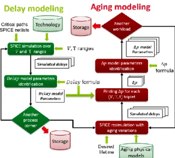
Off-line Modelling. The procedure is illustrated in Figure
1. One or more critical path netlists are extracted from the circuit design. . Note that previous works address the selection of the aging-aware representative paths [5]. The choice of how many and which paths must be selected is not addressed here. The netlists are then simulated within pre-defined 𝑉, 𝑇 ranges using. The resulting propagation delays are gathered and fitted with a 𝐷𝑒𝑙𝑎𝑦 model that depends on 𝑉 and 𝑇. This procedure is repeated for other process corners so that a set of parameters for the 𝐷𝑒𝑙𝑎𝑦 model is obtained and stored for each “path-corner” pair.
The next step consists in re-simulating all paths with aging-induced variations. As the propagation delay gets larger over time, it implies that there is at least one parameter of the 𝐷𝑒𝑙𝑎𝑦 model that evolves with aging. This parameter shift ∆𝑝 is evaluated by fitting the aged path delays with the 𝐷𝑒𝑙𝑎𝑦 model and comparing the resulting parameters with the fresh ones. The obtained ∆𝑝 are then fitted in an aging formula that depends on 𝑉, 𝑇 and on the power-on time (𝑡).
Finally, for a given application, the impact of the workload on aging is obtained using a cycle and bit accurate simulator tool. This tool provides both the circuit signal probabilities and the toggle rate for each circuit signal. The first one is an indispensable factor for estimating BTI degradation while the second one impacts mostly HCI.
The previous procedure is repeated for different workloads so that a set of parameters is stored for each “path-workload” pair.
On-line Estimation. First, local process variations are
characterized to calibrate the 𝐷𝑒𝑙𝑎𝑦 model parameters, i.e. to choose the appropriate one. This can be done with a Process-Control Monitor structure, for instance the one proposed in [6]. Then, voltage and temperature dynamic variations are periodically recorded to keep ∆𝑝 up-to-date using in-situ monitors, e.g. similar to [7]. Finally, whenever a new workload starts running, its respective ∆𝑝 parameters are loaded. This procedure is illustrated in Figure 2. When an information about the circuit condition is required, ∆𝑝 is calculated and then added to the respective parameters in the 𝐷𝑒𝑙𝑎𝑦 model. At the end, the 𝐷𝑒𝑙𝑎𝑦 value is calculated with and without ∆𝑝 in order to obtain the delay shift ∆𝐷𝑒𝑙𝑎𝑦 due to aging. Both ∆𝑝 and 𝐷𝑒𝑙𝑎𝑦 computations can be done at software-level since they do not require to be constantly
performed. However, a dedicated hardware module can also be envisaged.
III. APPLICATION
The proposed methodology has been validated on two different circuit architectures, namely, a DSP [8] and a RISC processor [9]. Both circuits have been implemented in 28nm FDSOI technology. Their architectures are depicted in Figure 3. Their critical paths have approximately 10 and 35 stages, respectively. Simulations were conducted using V and T ranges of [0.8, 1.4] V and [0, 150] ºC respectively, and a lifetime of 20 years. At total, 1573 (𝑉, 𝑇, 𝑡) conditions were
Figure 1. Methodology for obtaining a circuit-level aging model from device-level models. The first step consists in generating a propagation delay model 𝐷𝑒𝑙𝑎𝑦(𝑉, 𝑇). Aging simulations are then conducted to find the parameter shift ∆𝑝. A ∆𝑝(𝑉, 𝑇, 𝑡) formula is constructed at the end. All parameters from both 𝐷𝑒𝑙𝑎𝑦 and ∆𝑝 formula are stored to be used during circuit operation.
Figure 2. On-line estimation of circuit degradation from previously created models. Process calibration is done only once at the beginning of circuit lifetime. 𝑉, 𝑇 and workload are constantly monitored to keep ∆𝑝 up-to-date. Both 𝐷𝑒𝑙𝑎𝑦 and ∆𝐷𝑒𝑙𝑎𝑦 are calculated upon request, the last being the delay shift induced by BTI/HCI effects (∆𝑝).
Figure 3. Case-study architectures used to validate the proposed methodology. Top: 32-bits VLIW DSP, dedicated to Telecom applications [8]. Bottom: 32-bits RISC Harvard architecture, in-order, mono-thread, 5-stage pipeline [9].
simulated. The 𝐷𝑒𝑙𝑎𝑦 equation adopted here is based on Sakurai’s alpha power-law model [10]:
𝐷𝑒𝑙𝑎𝑦(𝑉, 𝑇) = 𝑝𝛽+ 𝑝𝜇−1(𝑇) ∗ 𝑉
(𝑉 − 𝑝𝑉𝑡ℎ(𝑇))𝑝𝛼 (1)
where 𝑝𝛽 and 𝑝𝛼 are constant while 𝑝𝜇−1(𝑇) and 𝑝𝑉𝑡ℎ(𝑇) are
exponential dependent on temperature and related to the transistors mobility and threshold voltage, respectively:
𝑝𝜇−1(𝑇) = 𝐶𝜇+ 𝑘𝜇∗ 𝑇𝑛𝜇 (2) 𝑝𝑉𝑡ℎ(𝑇) = 𝐶𝑉𝑡ℎ− 𝑘𝑉𝑡ℎ∗ 𝑇
𝑛𝑉𝑡ℎ
(3) A set of identified parameters for a particular path of the RISC processor is shown in Table 1. SPICE simulations with aging variations were then conducted through Eldo UDRM (User-Defined Reliability Model) API [11]. This tool computes the stress experienced by each transistor during a transient simulation and then performs a new simulation taking into account the resulting degradation. Physical models for BTI and HCI effects are used by the API to compute the degradation endured by the transistors [4]. The CPU times to simulate 1573 (𝑉, 𝑇, 𝑡) conditions for a path for the DSP and the RISC processor were 224 min and 682 min, respectively.
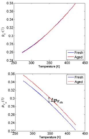
The aged path delays were then fitted to the 𝐷𝑒𝑙𝑎𝑦 model and new parameters were estimated. As expected, the parameter which evolves with aging is the one related to the
threshold voltage 𝑝𝑉𝑡ℎ, as can be seen in Figure 4. A parameter shift ∆𝑝𝑉𝑡ℎ was then obtained for each (𝑉, 𝑇, 𝑡)
condition. Figure 5 shows an example of ∆𝑝𝑉𝑡ℎ surface for a power-on time of 20 years.
All obtained ∆𝑝𝑉𝑡ℎ were gathered and fitted to a model
constructed from aging models found in the literature [12]: ∆𝑝𝑉𝑡ℎ(𝑉, 𝑇, 𝑡) = 𝑉𝛾 ∗ 𝑒
−𝐸𝑎
𝑘𝑇 ∗ (𝑐1∗ 𝑡𝑛1+ 𝑐2∗ 𝑡𝑛2) (4) where 𝛾 is the voltage acceleration factor, 𝐸𝑎 is the
temperature activation energy and 𝑘 is the Boltzmann’s constant. Note that this equation has two different time exponents (𝑛1, 𝑛2) since it models both BTI and HCI
phenomena which have different time dynamics. Table 2 presents a set of parameters identified for a path of the RISC processor.
Figure 4. Evolution of 𝑝𝜇−1(𝑇) and 𝑝𝑉
𝑡ℎ(𝑇) from a fresh situation to an aged
one (10 ys, 150ºC, 1.2V). There is no significant change of 𝑝𝜇−1, while 𝑝𝑉 𝑡ℎ
shows a shift due to aging (∆𝑝𝑉𝑡ℎ).
Table 1. A set of parameters for the 𝐷𝑒𝑙𝑎𝑦(𝑉, 𝑇) formula and their respective standard deviations. The ranges used for 𝑉, 𝑇 are [0.8, 1.4] V and [0, 150] ºC.
Table 2. A set of parameters for the ∆𝑝𝑉𝑡ℎ(𝑉, 𝑇, 𝑡) model and their respective
standard deviations. There are two different time exponents since BTI and HCI phenomena have different time dynamics.
Figure 6 shows an example of ∆𝑝𝑉𝑡ℎ evolution over time
for both case-study architectures. Even though both curves have similar behaviors over time, the resulting degradation is not the same. Finally, the computed ∆𝑝𝑉𝑡ℎ is integrated to the
𝐷𝑒𝑙𝑎𝑦 model to obtain the path propagation delay taking aging into account:
𝐷𝑒𝑙𝑎𝑦(𝑉, 𝑇, 𝑡) = 𝑝𝛽+
𝑝𝜇−1(𝑇) ∗ 𝑉
(𝑉 − (𝑝𝑉𝑡ℎ(𝑇) + ∆𝑝𝑉𝑡ℎ(𝑉, 𝑇, 𝑡))𝑝𝛼 (5)
The increase of the propagation delay due to aging can be obtained by computing the 𝐷𝑒𝑙𝑎𝑦 value with ∆𝑝V𝑡ℎ (5) and
without it (1) and comparing them. In Figure 7, ∆𝑝𝑉𝑡ℎ has
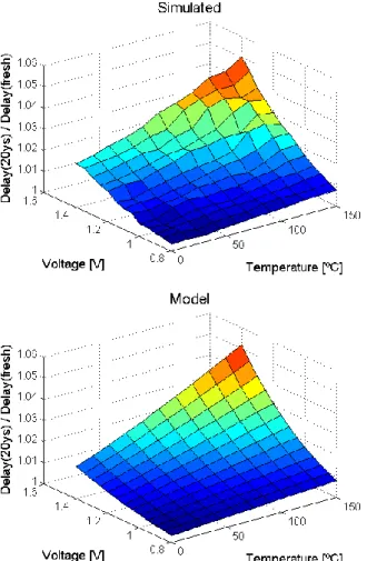
been integrated to the 𝐷𝑒𝑙𝑎𝑦 model to obtain the surfaces of delay degradation for a power-on time of 20 years. Note that the same 𝑉, 𝑇 conditions were used for both delay and aging calculation, this is why there is almost no degradation at low 𝑉 and 𝑇. Figure 8 shows similar surfaces but for a fixed ∆𝑝𝑉𝑡ℎ
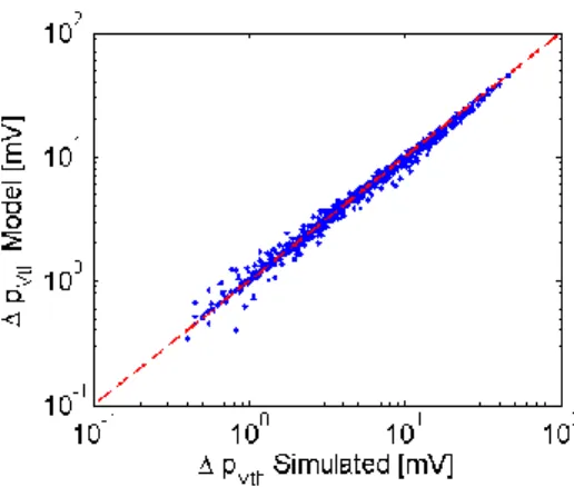
corresponding to a stress condition of 1.2V, 125ºC and 20 years. In this case the worst degradation is observed at low 𝑉. The degradation surfaces obtained using the proposed model is almost identical to the ones obtained through simulations. The ∆𝑝𝑉𝑡ℎ model accuracy has been verified for different
paths and stress conditions, as shown in Figure 9.
Figure 7. Degradation surfaces constructed through SPICE simulations (top) and the proposed models (bottom) for a power-on time of 20 years. The 𝑉, 𝑇 conditions are the same for both delay and aging, this is why there is almost no degradation at low 𝑉 and 𝑇.
Figure 6. ∆𝑝𝑉𝑡ℎ evolution over time for both DSP [1] (blue) and RISC
processor [2] (red). Stress conditions are 1.4V, 120º C.
Figure 8. Similar to Figure 7, degradation surfaces constructed through SPICE simulations (top) and the proposed models (bottom) but with a fixed
Lastly, dynamic variations have to be taken into account since this model will be used on-line. To handle voltage variations, we applied a similar method to the one in [13], as depicted in Figure 10. At a voltage change from 𝑉1 to 𝑉2,
firstly ∆𝑝𝑉𝑡ℎ(𝑉1, 𝑡1) is calculated, where 𝑡1 is the time spent at
𝑉1. Next, the inverse of the function is applied to compute 𝑡+,
the time required to have the equivalent ∆𝑝𝑉𝑡ℎ but with 𝑉2:
𝑡+= ∆𝑝
𝑉−1𝑡ℎ ⇔ ∆𝑝𝑉𝑡ℎ(𝑉2, 𝑡+) = ∆𝑝𝑉𝑡ℎ(𝑉1, 𝑡1 ) (6)
The final parameter shift ∆𝑝𝑉𝑡ℎ is then computed
considering the time spent at 𝑉2 plus 𝑡+:
∆𝑝𝑉𝑡ℎ = ∆𝑝𝑉𝑡ℎ(𝑉2, 𝑡2+ 𝑡+)
The same procedure is adopted for workload changes. In this case, the inverse of the function is computed using the corresponding parameters of the new workload.
For temperature variations, a simple weighted average is adopted instead. Note that, even though ∆𝑝𝑉𝑡ℎ has an
exponential dependence on 𝑇, it has a linear behavior within a limited temperature range.
IV. CONCLUSION
This work proposes a new bottom-up approach for on-line estimation of circuit degradation. Built on the top of device-level models, it takes into account all factors that impact global circuit aging, namely, process, topology, workload, voltage and temperature variations.
The proposed ∆𝑝𝑉𝑡ℎ model allows an accurate evaluation
of the degradation of the circuit critical paths during its operation. The model is fed by voltage and temperature monitors that on-line track dynamic variations. Finally, reliability strategies making use of this information can be implemented on-the-fly to increase circuit lifetime.
Future work directions will consider the implementation costs of the proposed on-line estimation in a real system. This includes how the 𝐷𝑒𝑙𝑎𝑦 and the ∆𝑝𝑉𝑡ℎ will be computed and
how much resources is needed for it. In addition, the effects of body bias changes in FDSOI UTBB technology is under study and will be included in both models.
ACKNOWLEDGMENT
This work has been partly funded by the BENEFIC project from CATRENE (CA505), and by the THINGS2DO project, co-funded by grants from France and the ECSEL Joint Undertaking (nb 621221).
REFERENCES
[1] X. Wang et al., “Silicon odometers: Compact in situ aging sensors for robust system design,” IEEE Micro, vol. 34, 2014.
[2] O. Heron, C. Sandionigi, E. Piriou, S. Mbarek and V. Huard, "Workload-dependent BTI analysis in a processor core at high level," IEEE International Reliability Physics Symposium, Monterey, CA, 2015, pp. CA.6.1-CA.6.6.
[3] T. Grasser et al., "The Paradigm Shift in Understanding the Bias Temperature Instability: From Reaction–Diffusion to Switching Oxide Traps," in IEEE Transactions on Electron Devices, vol. 58, no. 11, pp. 3652-3666, Nov. 2011.
[4] F. Cacho, P. Mora, W. Arfaoui, X. Federspiel and V. Huard, "HCI/BTI coupled model: The path for accurate and predictive reliability simulations," 2014 IEEE International Reliability Physics Symposium, Waikoloa, HI, 2014, pp. 5D.4.1-5D.4.5.
[5] C. Sandionigi and O. Heron, "Identifying aging-aware representative paths in processors," 2015 IEEE 21st International On-Line Testing Symposium (IOLTS), Halkidiki, 2015, pp. 32-33.
[6] B. P. Das, B. Amrutur, H. S. Jamadagni, N. V. Arvind and V. Visvanathan, "Within-Die Gate Delay Variability Measurement Using Reconfigurable Ring Oscillator," in IEEE Transactions on Semiconductor Manufacturing, vol. 22, no. 2, pp. 256-267, May 2009. [7] L. Vincent, E. Beigne, S. Lesecq, J. Mottin, D. Coriat and P. Maurine,
"Dynamic Variability Monitoring Using Statistical Tests for Energy Efficient Adaptive Architectures," in IEEE Transactions on Circuits and Systems I: Regular Papers, vol. 61, no. 6, pp. 1741-1754, June 2014. [8] C. Bechara, A. Berhault, N. Ventroux, C. Chevobbe, Y. Thuillier, R.
David and D. Etiemble, “A Small Footprint Interleaved Processor for Embedded Systems”, in Proc. International Conference on Electronics, Circuits and Systems (ICECS), December 2011, Beirut, Lebanon. [9] E. Beigné et al., "A 460 MHz at 397 mV, 2.6 GHz at 1.3 V, 32 bits
VLIW DSP Embedding F MAX Tracking," in IEEE Journal of Solid-State Circuits, vol. 50, no. 1, pp. 125-136, Jan. 2015.
[10] T. Sakurai and A. R. Newton, "Alpha-power law MOSFET model and its applications to CMOS inverter delay and other formulas," in IEEE Journal of Solid-State Circuits, vol. 25, no. 2, pp. 584-594, Apr 1990. [11] M. Selim, E. Jeandeau and C. Descleves, “Design–Reliability Flow and
Advanced Models Address IC-Reliability Issues”, in Workshop on Early Figure 9. Example of ∆𝑝𝑉𝑡ℎ obtained through simulations with physical
BTI/HCI models (x-axis) and through the proposed ∆𝑝𝑉𝑡ℎ model (y-axis).
Reliability Modeling for Aging and Variability in Silicon Systems @ DATE, March 2016, Dresden, Germany.
[12] X. Wang, P. Jain, D. Jiao and C. H. Kim, "Impact of interconnect length on BTI and HCI induced frequency degradation," 2012 IEEE International Reliability Physics Symposium (IRPS), Anaheim, CA, 2012, pp. 2F.5.1-2F.5.6.
[13] V. B. Kleeberger, M. Barke, C. Werner, D. Schmitt-Landsiedel and U. Schlichtmann, “A compact model for NBTI degradation and recovery under use-profile variations and its application to aging analysis of digital integrated circuits”, Microelectronics Reliability, Volume 54, Issues 6–7, June–July 2014, Pages 1083-1089.