HAL Id: tel-02476909
https://tel.archives-ouvertes.fr/tel-02476909
Submitted on 13 Feb 2020
HAL is a multi-disciplinary open access
archive for the deposit and dissemination of
sci-entific research documents, whether they are
pub-lished or not. The documents may come from
teaching and research institutions in France or
abroad, or from public or private research centers.
L’archive ouverte pluridisciplinaire HAL, est
destinée au dépôt et à la diffusion de documents
scientifiques de niveau recherche, publiés ou non,
émanant des établissements d’enseignement et de
recherche français ou étrangers, des laboratoires
publics ou privés.
New FDSOI-based integrated circuit architectures
sensitive to light for imaging applications
Lina Kadura
To cite this version:
Lina Kadura. New FDSOI-based integrated circuit architectures sensitive to light for imaging
ap-plications. Micro and nanotechnologies/Microelectronics. Université Grenoble Alpes, 2019. English.
�NNT : 2019GREAT031�. �tel-02476909�
THÈSE
Pour obtenir le grade de
DOCTEUR DE LA COMMUNAUTE UNIVERSITE
GRENOBLE ALPES
Spécialité : Nano Electronique et Nano Technologies
Arrêté ministériel : 25 mai 2016
Présentée par
Lina KADURA
Thèse dirigée par Alexei TCHELNOKOV, CEA-LETI, et
co-encadrée par Olivier ROZEAU, CEA-LETI et Laurent
GRENOUILLET, CEA-LETI
préparée au sein du Laboratoire d'électronique et des
technologies de l'information (CEA-LETI)
dans l'École Doctorale électronique, électrotechnique,
automatique et traitement du signal (EEATS)
Études de nouvelles architectures de
composants intégrés sensibles à la
lumière en filière FDSOI pour les
applications de type imageur
Thèse soutenue publiquement le 07/06/2019,
devant le jury composé de :
Pr. Pierre MAGNAN
Professeur des Universités, ISAE Toulouse, Toulouse (Rapporteur)
Dr. Yang Ni
CTO à New Imaging Technologies, Paris area (Rapporteur)
Pr. Albert THEUWISSEN
Professeur des Universités, TU Delft, Pays-Bas (Examinateur)
Pr. Francis CALMON
Professeur des Universités, INSA de Lyon, Lyon (Président)
Dr. Frederic LALANNE
Ingénieur de recherche à STMicroelectronics, Crolles (Examinateur)
Dr. Alexeï TCHELNOKOV
AKNOWLEDGEMENTS
I conducted my three years thesis research at LETI, in the advanced CMOS integration laboratory (LICL) in CEA-Grenoble. One of the best assets of LETI is the availability of experts that are always willing and benevolent to help and share their knowledge on the campus. Thanks to them I was able to learn and develop many new competences, so I’d like to start by thanking all the people at LETI that helped me achieve this work.
I’d like to thank the members of my jury, Pr. Pierre Magnan, Dr. Yang Ni, Pr. Francis Calmon, Pr. Albert Theuwissen, and Dr. Frederic Lalanne, for reading my manuscript, attending the defense and for all the positive and important feedback that helped me increase the quality of this manuscript. It was an honor having you all in my jury.
My warmest gratitude to my supervisors: Olivier Rozeau, SPICE modeling master, thank you for your guidance despite me “Papillonner” way too much, and for answering my questions during the countless times I entered your office saying “Olivier, j’ai une question” (I never had only one question though). Thank you for challenging me and demanding rigor in my work, helping me become a much better researcher. Laurent Grenouillet, process integration master, thank you for the good vibes ;), your constant enthusiasm which always motivated me to do better, and for your encouragement and support. I learned the benefit of having a positive critical thinking from you. Thank you also for the “end of contract-defense” period where you were always responding and available to discuss the manuscript/poster/paper (or to listen to me complaining) at the rdc of the bcc building. My thesis director Alexei Tchelnokov for all your encouragement and advices, and for being available to participate to our periodic meetings and enriching the discussion every time. Finally, thank you all three for the guidance and the rehearsals and review of paper/manuscript/presentations, I learned so much during these three years thanks to you. I hope I’ll have the pleasure of working with you all again in the future!
I’d like to thank my manager, Maud Vinet, for welcoming me in the LICL, and for your encouragement throughout the thesis. Thank you, the early morning technician team, Claude, Jean-Mi, Marie-Pierre, and Paul, for all the good memories around a nice Nespresso. Special thanks to Claude with whom I shared the office for three years. Thank you for all the conversations on variable topics, all the French grammar/movies/books/singers 70s pop culture knowledge that you shared with me (whether I wanted or not ;)). Thank you Louis (waaw), for genuine funny, interesting conversations. Thanks to all the people in the lab that I interacted with, whether it was in meetings, lunch, coffee or just discussions in the office: Bernard, Christophe, Valerie, Zdeneck, Hervé, Yves, Cyrile, Claire, Perrine, François, Laurent, Nils, Alexandre L, Sylvain, Laurent and Jean-Pierre. The electrical tests team: Jean and Alex V (you guys will always be my first mentors), Denis for your help with the IPE and all the fruitful discussions, Niccolo for negotiating on the equipment’s and wafers, Jacque, Xavier, Alain, Charles, the phd community Ilias, Artemisia, and Kostas (aka Istanbul) for making me a café frappé whenever I wanted one, and for the support through a good laugh whenever I had problems with my tests. Thank you Pascal Scheiblin from the simulation lab for your help with Silvaco and the VWF, and Christophe Licitra for the last minute simulations.
Page|6
Thank you the Padawan team of the LICL that gave meso many wonderful memories of these three years spent in the lab. The old generation: Julien, Alex, Mathilde, Jose, thank you guys for the pause café, the magic music quiz, and for making me feel part of the team right away. Rémy-sempai, who I would ask questions instead of opening a book on semiconductor physics and thanks to whom I learned so much from new French vocabulary to animals walk…whatever. Luca (thanks for the Loacker!), Vincent (secret kawai at heart), Sotiris (Café frapé), Benoit, Corentin, Loic, and Fabien. My generation: Jessy (rose et papillon), Thomas, and Carlos, we made it! Thank you guys for the support, discussions, breaks, and advice. The new generation: Giulia (girls power!) thank you for being an example of confidence, and inspiring me to become stronger, Camila with whom it was a pleasure sharing the same office, thank you for your support during the difficult time that are deadlines, and for the encouragement and discussions, just chill you’re going to do great ;), Daphnée, zen and give you a sense of zénitude, thanks for your cheerfulness and the good laughs, Mariia, Elizabeth, Louise, for sharing the office for short yet memorable periods of time. I wish to all of you the best of the best in life.
Thank you Marie, Faiza, and Amna for always maintaining my nostalgia for the other side of the Mediterranean Sea, and to Yumi-chan for maintaining my nostalgia for an even further away side. My best friends in Libya: Tasnim, Rawad, Elham, Nouran, and Arwa, who didn’t loosen their support and encouragement even though I missed all their important events. Thank you for everything guys, I’ve missed you a lot and I’ll see you soon!
I’d like to thank my family for their support throughout my education. Thank you, aunts, uncles, and cousins in France and Libya. Special thanks to tata Salha for listening to me complaining and worrying during these 3 years, and for attending my defense. Thanks mom and dad, for your unconditional support and constant encouragement, my brothers Marwan, Hicham, Sofian, Yazid, and Walid, my Sis-in-law Hamida and my niece Boubou. You guys always find a way to make me laugh away all my problems.
Finally, thank you everyone that helped me succeed and get where I am today.
Sincerely Lina Kadura
TABLE OF CONTENT
AKNOWLEDGEMENTS...5
TABLE OF CONTENT ...9
GLOSSARY ...15
INTRODUCTION ...19
CHAPTER 1 : IMAGE SENSORS AND LIGHT DETECTORS ...25
1.1.
S
TANDARD CAMERA SYSTEM... 27
1.1.1. CMOS VS CCD ... 28
1.1.2. CMOS IMAGE SENSORS STANDARD ARCHITECTURES ... 29
1.1.2.1. Passive Pixel Sensor (PPS) ... 29
1.1.2.2. Active Pixel Sensor (APS) ... 29
1.1.2.3. Digital Pixel Sensor (DPS) ... 30
1.1.2.4. Standard pixel operation ... 31
1.2.
P
IXEL DESIGN:
KEY PARAMETERS AND ARCHITECTURES... 31
1.2.1. PIXEL PARAMETERS ... 32
1.2.1.1. Size & Fill Factor (FF) ... 32
1.2.1.2. Sensitivity & Quantum efficiency ... 33
1.2.1.3. Dynamic Range, Conversion Gain, and Full Well Capacity ... 33
1.2.1.4. Noise parameters ... 34
1.2.1.4.a. Dark current ... 35
1.2.1.4.b. Reset kTC noise... 36
1.2.1.4.c. FPN ... 36
1.2.1.4.d. Correlated Double Sampling (CDS) ... 37
1.2.2. PROCESS INTEGRATION OPTIMIZATION ... 37
1.2.2.1. Back Side Illumination ... 37
1.2.2.2. 3D stack ... 38
1.2.3. SMALL PIXEL ARCHITECTURES ... 38
1.2.3.1. Shared transistors architecture ... 39
1.2.3.2. 1T pixel sensors ... 39
1.2.4. PIXEL ARCHITECTURES FOR DR EXTENSION ... 41
1.2.4.1. Logarithmic pixel sensor ... 41
1.2.4.2. Linear-Logarithmic pixel sensors ... 42
1.2.4.3. Others HDR techniques ... 43
TABLE OF CONTENT
Page|10
1.3.1.1. Machine vision and 3D imaging ... 45
1.3.1.2. LiDAR ... 45
1.3.2. COMPUTATIONAL IMAGING AND SMART SENSORS ... 46
1.3.2.1. Event based smart image sensors ... 46
1.4.
C
HAPTER ONE SUMMARY... 48
CHAPTER 2 : NEW FDSOI BASED PIXEL SENSOR (FDPIX)...57
2.1.
FDP
IX:
A NEW PIXEL SENSOR... 58
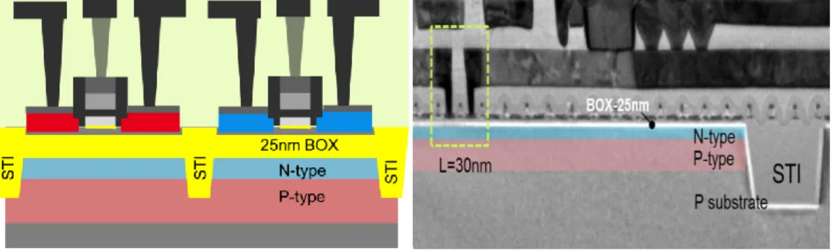
2.1.1. PIXEL STRUCTURE DESCRIPTION ... 58
2.1.1.1. Fully Depleted Silicon-On-Insulator (FDSOI) transistor ... 58
2.1.1.2. FDSOI/photodiode integration ... 59
2.1.1.2.a. STI for pixel isolation ... 60
2.1.1.2.b. Floating node and well connection for back bias ... 60
2.1.2. OPERATION PRINCIPLE... 60
2.1.2.1. FDPix and the Light Induced VT Shift (LIVS) ... 60
2.1.1.1. Modeling of the DC response ... 62
2.1.1.1.a. FDSOI capacitive coupling ... 62
2.1.1.1.b. Photodiode ... 67
2.1.1.2. FDPix response to light: LIVS vs optical power ... 75
2.1.1.3. Impact of light on transistor characteristics ... 77
2.1.1.3.a. MOSFET IDVG and IDVD ... 77
2.1.1.3.b. Subthreshold swing (SS) ... 78
2.1.1.3.c. LIVS calculation from ID ratio and SS ... 79
2.1.3. PROCESS FLOW ... 80
2.1.3.1. SOI SmartCut process ... 80
2.1.3.2. FDPix process flow ... 81
2.2.
C
OMPLEMENTARYFDP
IX SENSORS... 85
2.2.1. NMOS AND PMOS PIXELS ... 85
2.2.2. PHOTODIODE ORIENTATION ... 85
2.3.
C
HAPTER TWO SUMMARY... 86
CHAPTER 3 : TRANSIENT ANALYSIS: DYNAMIC RESPONSE AND RESET ...93
3.1.
FDP
IX TRANSIENT COMPONENTS... 94
3.1.1. FDSOI TRANSISTOR CAPACITANCE NETWORK... 95
3.1.2. PHOTODIODE EQUIVALENT RC CIRCUIT ... 96
3.1.3. FDPIX CAPACITANCE NETWORK ... 100
3.2.
FDP
IX TRANSIENT CHARACTERISTICS... 101
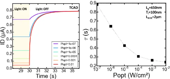
3.2.1. RISE TIME (LIGHT ON) TRANSIENT ... 101
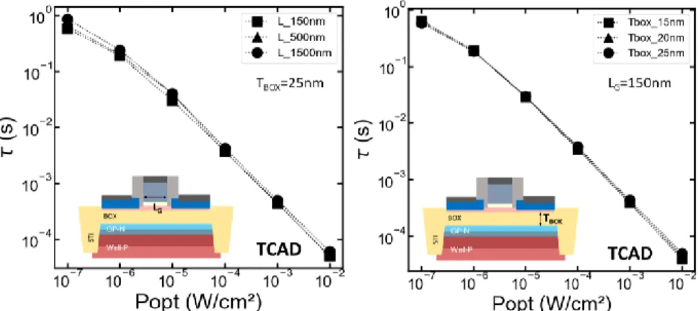
3.2.1.2. Dependence on transistor parameters (LG, TBOX) ... 103
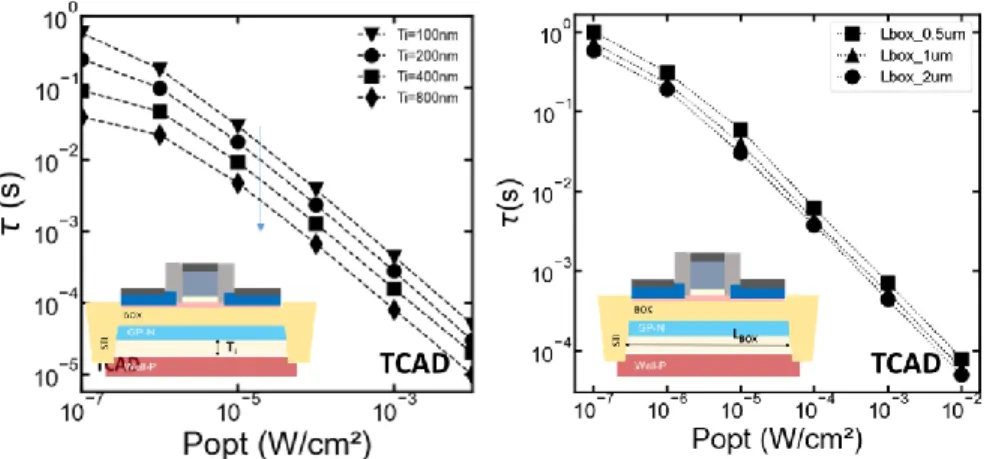
3.2.1.3. Dependence on diode parameters (Ti, LBOX) ... 104
3.2.2. FALL TIME (LIGHT OFF) TRANSIENT ... 105
3.2.2.1. Dependence on diode parameters (Ti) ... 106
3.3.
R
ESET OPERATION ANDFDP
IX DYNAMIC RESPONSE... 106
3.3.1. FDPIX RESET USING BACK BIAS ... 107
3.3.1.1. FDPix response to reset pulse in dark: Capacitive divider ... 108
3.3.1.2. FDPix response to reset pulse under light illumination ... 111
3.3.1.2.a. Reset after light turned off ... 111
3.3.1.2.b. Reset under constant light illumination ... 113
3.3.2. REGIONS OF OPERATION ... 115
3.3.2.1. Steady state mode (logarithmic response) ... 115
3.3.2.2. Integration mode (linear-log response) ... 115
3.3.3. HISTORY EFFECT (LAG, RESIDUAL CHARGES) ... 116
3.4.
FDP
IX RESPONSE TO VARIABLE LIGHT ILLUMINATION... 118
3.5.
C
HAPTER THREE SUMMARY... 120
CHAPTER 4 : FDPIX OPTIMIZATION AND TRADEOFFS ...125
4.1.
I
NFLUENCE OF TECHNOLOGICAL AND OPERATION CONDITIONS... 126
4.1.1. TRANSISTOR BODY FACTOR ... 126
4.1.1 JUNCTION PARAMETERS ... 128
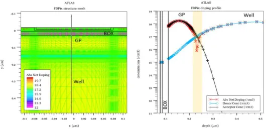
4.1.1.1 Doping profile ... 129
4.1.1.2 Junction leakage ... 132
4.1.1.1.a. Defect concentration ... 132
4.1.1.1.b. Temperature stability ... 133
4.1.2 IMPACT OF OPERATION CONDITIONS ON FDPIX PERFORMANCE ... 134
4.1.1.2. Reset pulse amplitude ... 134
4.1.1.3. Integration time ... 135
4.2.
L
IGHT DETECTION OPTIMIZATION... 136
4.2.1. FDPIX SPECTRAL RESPONSE ... 136
4.2.2. BACK SIDE ILLUMINATION (BSI) ... 139
4.2.2.1. TCAD simulation ... 140
4.2.2.2. Process flow ... 140
4.2.2.2.a. BSI integration using double BOX structure ... 140
4.2.2.2.b. BSI integration using P/P+ wafer structure ... 143
4.2.2.2.c. BSI process of FDPix without etch stop layer ... 143
4.2.3. U-SHAPE PHOTODIODE IMPLANTATION PROFILE ... 145
4.2.3.1. TCAD simulation ... 146
TABLE OF CONTENT
Page|12
4.2.4. THE FDPIX FOR MULTIPLE SPECTRUM DETECTION ... 147
4.3.
FDP
IX SCALING... 148
4.4.
C
HAPTER FOUR SUMMARY... 150
CHAPTER 5 : FDPIX-BASED PIXEL CIRCUIT DESIGN AND VALIDATION ...157
5.1.
FDP
IX COMPLEMENTARITY PROPERTY... 158
5.2.
A
NALOGFDP
IX... 159
5.1.1 CURRENT MODE PIXELS ... 159
5.1.2 SATURATED LOAD INVERTER AMPLIFIER ... 159
5.1.2.1 FDPix saturated load inverter: DC and transient characterization ... 161
5.1.2.2 Static power consumption ... 164
5.1.2.3 Minimum size implementation ... 166
5.1.3 PUSH PULL AMPLIFIER: CMOS INVERTER ... 167
5.1.3.1 FDPix light sensitive CMOS inverter: DC and transient characterization ... 170
5.1.3.2 Static power consumption ... 173
5.1.4 PIXEL ARRAY CONFIGURATION ... 174
5.1.5 CONCLUSION ON ANALOG PIXELS ... 175
5.3.
T
IME DOMAIN PIXELS... 176
5.3.1. PULSE WIDTH MODULATION (PWM) PRINCIPLE ... 176
5.3.2. THE PWM-BASED FDPIX SENSOR ... 177
5.3.3. PIXEL ARRAY CONFIGURATION ... 183
5.4.
A
NALOG ANDPWM-
BASED PIXEL SUMMARY... 184
5.5.
P
ERSPECTIVES TOWARDS LIGHT SENSITIVE LOGIC... 184
5.5.1. LIGHT SENSITIVE SRAM ... 185
5.5.2. LIGHT SENSITIVE GATES ... 186
5.6.
C
HAPTER FIVE SUMMARY... 189
CHAPTER 6 : CONCLUSION AND PERSPECTIVES ...195
6.1.
FDP
IX CHARACTERISTICS SUMMARY... 195
6.2.
F
UTURE WORK... 197
6.3.
P
ERSPECTIVES... 198
APPENDIX A : SIMULATION TOOLS AND SOFTWARE ...203
A.1.
TCAD
S
IMULATIONS... 203
A.2.
SPICE
SIMULATION... 205
B.1.
W
AFER PROBER... 208
B.2.
S
EMICONDUCTOR ANALYZER... 208
B.3.
M
ONOCHROMATOR AND LIGHT SOURCE SPECIFICATIONS... 208
B.4.
I
NSTRUMENTATION USINGP
YTHON ANDL
ABV
IEW... 209
APPENDIX C : EXTRA EXPERIMENTS AND RESULTS ...213
C.1.
FDP
IX SENSOR WITH RESET TRANSISTOR... 213
C.2.
PWM-
BASEDFDP
IX:
OTHER IMPLEMENTATION OPTIONS... 214
C.2.1. SERIES INVERTERS ... 215
C.2.2. SINGLE INVERTER AND COMPARATOR ... 215
LIST OF PUBLICATIONS ...217
GLOSSARY
List of Abbreviations
Acronym
Definition
AC
Alternative current
ADC
Analog-to-Digital Converter
ADAS
Advanced Driving Assistance System
AI
Artificial Intelligence
APS
Active Pixel Sensors
AR
Augmented Reality
ARC
Anti-Reflection Coating
BB
Back Bias
BEOL
Back End Of Line
BF
Body Factor
BOX
Buried OXide
BSI
Back Side Illumination
CCD
Charge Coupled Device
CDS
Correlated Double Sampling
CIS
CMOS Image Sensors
CMOS
Complementary Metal Oxide Semiconductor
CTRIM
Crystal-TRIM
DC
Direct Current
DCL
Duty Cycle
DPS
Digital Pixel Sensor
DR
Dynamic Range
DRAM
Dynamic Random Access Memory
DRC
Design Rule Checker
DRM
Design Rule Manual
DTI
Deep Trench Isolations
DUT
Device Under Test
GLOSSARY
Page|16
FDSOI
Fully Depleted Silicon On Insulator
FEOL
Front End Of Line
FF
Fill Factor
FoM
Figure of Merit
FPGA
Field-Programmable Gate Array
FPN
Fixed Pattern Noise
FSI
Front Side Illumination
FWC
Full Well Capacity
GND
Ground (reference zero)
GO1
Thin Gate Oxide
GO2
Thick Gate Oxide
GP
Ground Plane
HDR
High Dynamic Range
IR
Infrared
LIDAR
Light Detection and ranging
LIVS
Light Induced VT Shift
LVT
Low VT
MOSFET
Metal Oxide Semiconductor Field Effect Transistor
MtM
More than Moore
MUX
Multiplexer
NA
Numerical Aperture
NIR
Near Infra-Red
OBB
Optical Back Biasing
PD
Pull Down
PFM
Pulse Frequency Modulation
PM
Pulse Modulation
PPS
Passive Pixel Sensor
PU
Pull Up
PWM
Pulse Width Modulation
QE
Quantum Efficiency
RBB
Reverse Back Bias
RVT
Regular VT
SCE
Short Channel Effect
SNR
Signal to Noise Ratio
SOI
Silicon On Insulator
SPAD
Single Photon Avalanche Diode
SPICE
Simulation Program with Integrated Circuit Emphasis
SRAM
Static Random Access Memory
SS
Subthreshold Swing
STI
Shallow Trench Isolations
TEM
Transmission Electron Microscopy
ToF
Time of Flight
TSV
Through Silicon Via
UTBB
Ultra-Thin Body and BOX
VDD
Supply Voltage
VLC
Visible Light Communication
VR
Virtual Reality
GLOSSARY
INTRODUCTION
Today’s technology is moving towards enabling a smarter environment. Sensors are everywhere, and their number is expected to drastically increase in the future years. New applications englobed in the Moore’s law spin off, More-Than-Moore (MtM), have been demonstrated. Light sensors are major contributors to this evolution. Used primarily as image sensors, they now have evolved towards ambient intelligence application when used as motion, proximity, ambient light sensors and so on. The image sensor industry growth has not declined since the first camera was embedded in mobile phone that later became smartphones. The pixel size kept shrinking over the years and new technologies were developed to continue improving their performance. Today’s challenges regarding image sensors include high speed, high performance, small size and always less energy consumption. To achieve the aforementioned criteria, 3D stack technology of multiple layers, including the processing and memory layer on top of the sensor have been developed. To avoid complex process integration, planar embedded sensors, where the structure is by default 3D-like, will increase the ease of integration at a lower cost. Also allowing the use of more advanced technological nodes will not only reduce the pixel size, but also the power demands of the circuit. Finally, decoupling the sensing from the readout is an interesting solution to allow the optimization of both parts and expend the range of detection using the same readout circuit. It is in this context that falls the thesis topic.
A Light sensor based on the co-integration of a Fully Depleted Silicon-On-Insulator (FDSOI) transistor with a photodiode underneath the Buried Oxide (BOX) is thoroughly studied, simulated, and characterized. This sensor, called FDPix and shown in Figure I-1, features very small size, simplified process, and low power consumption. when illuminated, the photogeneration in the photodiode will modulate the transistor electrical characteristics by means of a capacitive coupling between the front and back interfaces. Therefore, no electrical connection is present nor needed between the sensing transistor and the photosensitive element for the device to operate. This maintains the size of the sensor minimum since it is composed of only one transistor.
The thesis was conducted at LETI, a French research institute located in Grenoble, France, that tremendously contributed to the development of the FDSOI technology, along with its regional partners, STMicroelectronics and SOITEC, in the 2005s. All the devices studied and characterized in this work were fabricated at STMicroelectronics using 28nm node FDSOI technology. In the view of MtM applications, and the proven performance of FDSOI in analog/RF sensors, this thesis topic follows this unstoppable trend of integrating more intelligence as close as possible to the sensor.
INTRODUCTION
Page|20
Figure I-1: FDPix sensor sideview, TEM image and schematic
Thesis organization:
Chapter 1 is dedicated to the state of the art of the field of image sensors. Starting with an economical and market view on the topic, it follows a presentation of the standard image sensor and the main figure of merits (FoM). Specific sensor architectures that optimize certain of these FoMs are also discussed, such as small pixel dimensions and logarithmic pixels. Finally, the main trending applications are briefly introduced and discussed based on the sensor architecture used.
Chapter 2 kicks off the investigation on the FDPix sensor. The main physical phenomenon characterizing the sensor operation in the DC domain are studied. The FDSOI transistor and the photodiode that forms the structure are modeled. Finally, the FDPix sensor is evaluated by considering the combination of the two. The DC characteristics are discussed using TCAD simulation and opto-electrical characterization of the fabricated devices. A fabrication flow is also presented highlighting the main step to be modified in the 28nm process flow to obtain our sensor. The chapter is concluded by introducing an important property of the FDPix based on Complementary Metal Oxide Semiconductor (CMOS) integration.
Chapter 3 continues the study of the response of the FDPix in the time domain. The equivalent capacitance network of the device is analyzed, and the response times of the sensor are characterized. A reset method is developed, and the transient response curve of the sensor discussed. We will show that a good agreement is obtained between the developed model implemented in SPICE environment and the electrical characterization. Finally, a test case with variable light stimuli is presented.
Chapter 4 presents the optimization of the FDPix technological and operational parameters in DC and transient domain. Both the transistor and photodiode are optimized, and the main tradeoffs are discussed. In this chapter, we also present different integration schemes investigated to optimize the device parameters, such as Back Side Illumination (BSI) and junction engineering. A conclusion on scaling effect on the device is drawn and summarized, as well as a perspective regarding the possible versatility of integration of the sensor.
Chapter 5 is design oriented. Different pixel architectures were designed, layouted, fabricated and tested. We divided them in two categories: analog pixels based on amplifier circuits, and digital-like pixels based on Pulse width
Modulation (PWM) and light sensitive inverters. The designed pixel circuits were proven to be functional. We conclude the chapter by presenting simulated and tested logic devices such as Static Random Access Memory (SRAM) and pass gates sensitivity to light illumination, which opens perspectives in smart sensor applications.
Chapter 6 ends the thesis manuscript with a general conclusion, and the major perspectives regarding the FDPix sensor.
Details regarding the simulation tools and models, as well as the characterization setup specifications and data processing codes are given in Appendix A and B. Appendix C presents extra pixel circuit configurations developed during this work.
CHAPTER ONE
CHAPTER 1 : IMAGE SENSORS AND LIGHT DETECTORS ...25
1.1.
S
TANDARD CAMERA SYSTEM... 27
1.1.1. CMOS VS CCD ... 28 1.1.2. CMOS IMAGE SENSORS STANDARD ARCHITECTURES ... 29
1.2.
P
IXEL DESIGN:
KEY PARAMETERS AND ARCHITECTURES... 31
1.2.1. PIXEL PARAMETERS ... 32 1.2.2. PROCESS INTEGRATION OPTIMIZATION ... 37 1.2.3. SMALL PIXEL ARCHITECTURES ... 38 1.2.4. PIXEL ARCHITECTURES FOR DR EXTENSION ... 41
1.3.
T
ECHNOLOGIES AND APPLICATIONS... 44
1.3.1. TIME OF FLIGHT (TOF) ... 44 1.3.2. COMPUTATIONAL IMAGING AND SMART SENSORS ... 46
IMAGE SENSORS AND LIGHT DETECTORS
Chapter 1 : Image Sensors and Light Detectors
The increase of user interactive applications is driving the semiconductor industry towards more heterogeneous technologies, in which both the analog sensing and digital processing are of equal importance. The scaling of the transistor dimensions following Moore’s law [MOORE 1998] and Dennard scaling [DENNARD 1974] allowed the digital
electronics applications to improve over the years. Digital circuits today demonstrate impressive performance with lower power consumption, and always smaller size. Due to the emergence of new fields of applications, and the evolution of the societal needs, the industry redefined the Moore’s law to englobe these new applications. Two subsets were defined (Figure 1-1). The “More Moore” section continues the scaling, or rather the effective scaling of the transistor using advanced material technology and processes. The size of the transistor is relatively constant, but its performance is still following the prediction using technology enabler elements (beyond CMOS). The second divergence from the Moore’s law is the More-than-Moore (MtM). The MtM deals with diversification based on an application-oriented technology development route, where the consumer is of major interest. MtM englobes applications enabling ambient intelligence that concerns health, mobility, communication, security, etc [ARDEN].
These applications are mainly in need of devices that interacts with the outside world. Therefore, it concerns analog and RF circuits, powering circuits, sensors and actuators, biochips and so on. The digital is no longer the driving force in MtM. However, for most of the applications, a heterogenous integration is necessary. In this category falls one of the major driving applications in the MtM, the CMOS Image Sensor (CIS).
Figure 1-1: The ITRS trends, towards miniaturization (More Moore) towards diversification (More-Than-Moore) [ARDEN]
The CIS is a heterogenous technology. The photon-to-electron conversion is performed by the pixel array, the readout is using analog amplifiers, and finally the image processing is performed on digital data. Since its development in the 90s, and due to the integration of the camera in the mobile phone in 2000, the CIS market has encountered a steady growth. As reported by [YOLE DEVELOPPEMENT 2018A], the CIS market is expected to grow from $16B in 2017 to
$24B in 2023, or as expressed in Figure 1-2 in terms of production volume [IBS2018]. Today, the mobile market is
IMAGE SENSORS AND LIGHT DETECTORS
Page|26
to feature Back-Side Illumination (BSI) combined with 3D stack process. Now the hybrid stack and multi-level stack have become the new trends. These technologies enabled new features such as slow motion and 3D imaging embedded in smartphones. These advances in CIS were enabled by the three key players that dominates the market, namely Sony (42%), Samsung (20%), and Omnivision (11%). They have been dominating the CIS market by developing BSI, 3D stack process and hybrid integration.
Figure 1-2: production volume of CMOS image sensors for different application segment [IBS2018]
Other domains of application have experienced an important growth during the past years. The automotive which is a major trend in the industry at the moment, experienced a 23% growth between 2016 and 2017. Security also have become a major contributor to the CIS market with a 26% growth. Finally, Artificial Intelligence (AI), Augmented Reality (AR) and Virtual Reality (VR) are applications that attract a lot of attention and are major contributors to the demands on CIS. The CIS ecosystem has indeed shifted from “vision for imaging to vision for sensing” (Yole) as depicted in Figure 1-3. All ambient intelligence application englobed in the MtM, are contributing to the constant demand of improved key metric performance of image sensors.
1.1. Standard camera system
A standard camera system is shown in Figure 1-4. The procedure of image capture can be described as follows: • The light (sun light or artificial) is reflected on the scene, and the incoming reflected waves interact with the
camera system by first being focused by the main camera lenses on the sensor. • The light is then focused on each photosite by means of microlenses present per pixel.
• Since the photosite detect only the brightness of the scene, each pixel has a color filter to discriminate the color. This is obtained by using a mosaic Bayer color filter [BAYER 1976], composed 50% of green pixels
and 25% red 25% blue. A demosaicing process1 is performed to process the raw data and obtain the final image.
• The monochromatic light penetrates the photosite where the conversion of photon-to-electron takes place due to the photoelectric effect. The photogenerated charges are then converted to a voltage analog output by analog amplifiers either located at the array level, or locally in the pixel.
• The analog voltage readout is further amplified and converted to digital data using an Analog-to-Digital Converter (ADC).
• The digital signal is further processed for error and noise correction and saved in a memory.
Figure 1-4: Standard color imaging camera system
The system shown and described is for visible light imaging. For other application targeting detection rather than color imaging, some component will differ, such as the presence or not of a color filter array. Also, the processing blocks will depend on the pixel architecture used. The pixel array is what ultimately determines the quality and efficiency of the system. We will present in the next sections a comparison between the two standard pixel technologies that dominated the market of digital imaging, namely the charge coupled devices (CCD) and the Complementary metal oxide semiconductor (CMOS) pixels.
IMAGE SENSORS AND LIGHT DETECTORS
Page|28
1.1.1. CMOS vs CCD
Up until the 90s, the image sensor industry was dominated solely by Charge-Coupled Devices (CCD) developed in the 70s. A CCD sensor consist in an array of MOS capacitors [HOWELL 2003] (Figure 1-5.a). When illuminated, the
photo-generated charges are collected in the potential well. Then the charges are readout within the array by sequentially biasing the gates of one column and are then converted to a voltage by an amplifier located outside the array. The advantages of the CCD are high quality/resolution imaging, high sensitivity, ~100% fill factor2 and low noise. However, the readout is slow due to serial readout, it has a dedicated process not compatible with standard CMOS process, which resulted in a relatively higher price.
The first CMOS image sensors (CIS) were developed in the 70s, where the pixel was composed of only a photodiode and one select transistor and was called Passive Pixel Sensor (PPS). Although offering a high FF, its noise performance much lower than CCD, prevented it to be considered for imaging. It is in the early 90s, when the CMOS Active Pixel Sensor (APS) was developed [FOSSUM 1993] that the CIS became a true competitor to CCD. In APS, the amplifier is
integrated per pixel resulting in a local charge-to-voltage conversion and a voltage readout (Figure 1-5.b). This inevitably increased the number of transistors per pixel which reduced the FF. However, its compatibility with standard CMOS process allowed the miniaturization and reduced the manufacturing cost. In CCD, since the charges photogenerated need to be transferred, it requires more power. Also, the readout is performed in series, which highly limits the sensor speed. It is also very sensitive to temperature variation and in some applications needs to be cooled. CIS allowed random access in the same way as Dynamic Random Access Memory (DRAM), where the voltage analog output is readout in parallel, which highly increases speed and decreased power consumption.
Figure 1-5:CCD vs CMOS image sensor pixel structure [HOWELL 2003][TURCHETTA]
Due to their superior performance and small size over CMOS, CCD dominated the market until early 2000s. In 2000, the first mobile phone featuring an embedded camera was developed by Sharp in Japan [DIGITALTRENDS 2013]. This
camera used a CMOS image sensor with 0.11-megapixel resolution. The main driver for developing CIS became the mobile device market. Starting from there, the potential of market growth for embedded camera was evident. In 2017 about 1.2 trillion digital pictures were taken and 85% of them using smartphones [STATISTICA 2017]. The sensor
requirement for mobile application are: small size, low cost, speed and low power. For all these properties the CIS surpassed the CCD. At the beginning of CIS era, the image quality was not comparable with CCD due to lower FF
and higher noise, but now with the advance in CMOS technology and image sensor technology improvement, CIS quality is as good as CCD if not better, for lower power consumption and high-speed imaging. Now the CMOS market surpasses the CCD as shown in Figure 1-6. However, CCD are still used in niche applications such as ultra-high-resolution applications, and ultra-low-light applications such as astrophotography. Since the market is moving towards smart sensing, there is no doubt that CIS will stay the main sensor used for future applications.
Figure 1-6: sales amount in the past years for CCD and CMOS [TERANISHI 2018]
In the following section of this chapter, the main CMOS sensor properties are discussed. We will present the most common architectures, as well as architectures that optimizes specific parameters such as size and Dynamic Range (DR).
1.1.2. CMOS image sensors standard architectures
1.1.2.1. Passive Pixel Sensor (PPS)
When the CIS was first developed in the 70s, it was as the passive pixel sensor (PPS) shown in Figure 1-7.a. This architecture is simple, it only contains a diode for detection and a transistor for row selection. Although being simple, this technology suffered from poor image quality, slow readout, and large noise resulting from the capacitive mismatch between the pixel and the column bus which resulted in high KTC noise. Therefore, the CCD dominated since it offered much better performance.
1.1.2.2. Active Pixel Sensor (APS)
The Active Pixel Sensor (APS) was first proposed by Noble in 1968 [NOBLE 1968], and more greatly studied under
this term, APS, in the 90s by Eric Fossum [FOSSUM 1993]. This architecture consisted in adding the column amplifier
per pixel to perform charge-to-voltage conversion locally. In this manner, a voltage output is readout instead of charge transfer. This resulted in reducing power consumption, random access, and high-speed readout. Although adding transistor per pixel reduced the FF, the improvement due to the advantages mentioned resulted in making this architecture the most widely used today. The first version of the APS consisted in three transistors per pixel (3T APS) and is shown in Figure 1-7.b, where a reset (RST), source follower (SF), and row select (SEL) transistors are
IMAGE SENSORS AND LIGHT DETECTORS
Page|30
a high reset noise. In early 80s, N.Teranishi developed the pinned photodiode [TERANISHI 1982] where a P+ layer is
implanted at the interface to passivate the Si/SiO2 interface states. This approach considerably reduced noise. Initially integrated for CCD devices, it was later used in CIS [FOSSUM 2014][GUIDASH 1997] which allowed considerable
reduction of dark current, increase of saturation level and improved sensitivity. It also resulted in using electronic shutter by using a transfer gate (TX) and a floating diffusion (FD) node. This architecture is shown in Figure 1-7.c. and is called the four transistor (4T) APS. The 4T APS architecture is the most used pixel sensor today. By decoupling the reset node from the sensing node, the reset noise was reduced. True Correlated Double Sampling (CDS) technique (section 1.2.1.4.d) can be implemented, and when complete charge transfer is achieved, the image lag3 is suppressed using this architecture.
Figure 1-7: Standard pixel architectures: a) PPS b)3T APS c)4T APS
1.1.2.3. Digital Pixel Sensor (DPS)
In the previously mentioned architectures, the output of the pixel is an analog voltage signal. After the readout this voltage is converted to digital data using an Analog-to-Digital Converter (ADC), which is usually located at the end of each column. The first developed Digital Pixel Sensor (DPS) was reported by [FOWLER 1994], where an ADC and
a memory node are implemented per pixel as shown in Figure 1-8. Integrating the ADC per pixel increases the Signal-to-Noise Ratio (SNR) by reducing readout noise, it increases the Dynamic Range4 (DR) since the signal swing is not limited by the supply, and allows high speed imaging (>10 kfps [KLEINFELDER 2001]). However, adding the ADC and
memory per pixel inevitably increased drastically the pixel size and lower its FF due to higher transistor count per pixel. For this reason, DPS are not used in consumer electronics market. Nevertheless, with the CMOS technology scaling, the FF of DPS improved. Also, obtaining a digital output allows increasing image processing functionality which made these pixels adequate for smart pixel applications, as discussed in section 1.3.2.1.
Figure 1-8: Standard DPS architectures
3Image lag is due to incomplete reset and thus results in presence of information from the previous frame 4Range of light intensities the sensor can detect and discriminate. It will be defined in detail in later sections.
1.1.2.4. Standard pixel operation
Figure 1-9 below shows the basic 3T APS voltage output, where the operation sequence is indicated and consists in three phases:
1. Reset phase (reset transistor ON) where the photodiode voltage is set to a reference voltage Vref.
2. Exposure phase (reset transistor OFF), where the photons are integrated in the photodiode capacitance during a fixed integration time (tint).
3. And readout (SEL and SF ON), where the voltage level is sampled and further processed at the column, chip, or off chip level.
Figure 1-9: standard CIS operation
Depending on the type of pixel and its response, more phases might be implemented. For example, a double reset scheme is used to perform noise canceling (CDS) in most sensor designs. Also, depending on the tint, more or less charges are collected which will affect the sensitivity and DR. An illustration of the ideal response vs optical power of a linear APS is illustrated in Figure 1-10 below. An ideal DR would be the whole intensity range before saturation, however, the minimum detectable level will depend on noise, as will be explained in further sections.
Figure 1-10: simplified illustration of linear image sensor response for different tint
1.2. Pixel design: key parameters and architectures
In this section, the main pixel sensor properties are presented. The discussion will include the geometrical, electrical and optical properties. The point is to be able to compare the different architectures proposed in the next section based on the presented properties.
IMAGE SENSORS AND LIGHT DETECTORS
Page|32
1.2.1. Pixel parameters
1.2.1.1. Size & Fill Factor (FF)
As previously mentioned, one of the main advantages of using CMOS compatible technology is the reduction in size following the scaling law [DENNARD 1974]. As shown in Figure 1-11, due to the shrink of transistor gate length and
development of advanced process node, the pixel size was reduced, and the power consumption lowered. Today, commercialized consumer electronics pixels are in the micron range. However, the CMOS process evolution could not be directly used in CIS. The high leakage at small dimension, and the dielectrics used in Back End Of Line (BEOL), are some of the reasons that led to the development of a process specific to CIS. As can be observed on Figure 1-11, there is a gap between the CIS process and the main stream CMOS process of about three generations [THEUWISSEN
2007] however the scaling rate is almost identical.
Figure 1-11: scaling of APS [THEUWISSEN 2007]
Also, using Front Side Illumination (FSI) configuration where the pixel is illuminated from the top through the metal layers, with the increase of pixel density the metallization design has become more difficult to deal with. The distance between metal lines is shortened and the light path focused by the micro-lenses might get reflected on the metal lines which causes crosstalk. Therefore, other solutions have been proposed such as integrating waveguides between the microlens and the photodiode to obtain better focus of the light [AGRANOV 2009][LEE 2019]. However, the best
solution came as a natural evolution, consisting in Back Side Illuminated (BSI) sensor, where the light is incident on the back surface of the sensor after thinning it down. The BSI process is discussed in more details in section 1.2.2.1 and in Chapter 4.
The reduction in pixel size results in better spatial resolution at the expense of lower sensitivity. Also, the Signal to Noise ratio (SNR) will be lower due to smaller pixel area and thus less photon absorbed. Reducing the pixel size will also affect the Full Well Capacity (FWC) and thus the DR. All these parameters will be presented in the following sections.
Another important parameter related to the pixel size and scaling is the Fill Factor (FF). FF is defined as the ratio or percentage of photosensitive area to the total pixel area (Figure 1-12.a). It represents how much of the total pixel area
is used to collect photons, or inversely the area that is shadowed by either transistors or metal lines. A high FF results in a higher sensitivity since more charges are collected by the pixel, therefore it should be maximized. Since the pixel transistors followed the scaling law, their dimensions were reduced which allowed the improvement of the FF. To overcome the reduced FF, micro-lenses are added to the pixel to focus the light on the photodiode area and reduce optical cross talk between pixels as illustrated in Figure 1-12.b.
Figure 1-12: a) Schematics showing the reduction of FF by adding transistors/pixel b) The use of micro lenses to increase the FF [HAMAMATSU]
1.2.1.2. Sensitivity & Quantum efficiency
The sensitivity of a linear response sensor such as the 3T-4T APS, is defined as the slope of the transfer function in V/lux.s or e-/lux.s. It represents the potential change for a given light intensity and integration time. Therefore, it is highly dependent on the Quantum efficiency (QE) of the sensor.
The QE is what quantifies how efficiently the incident photons are collected and converted to electrons. It is wavelength dependent since it depends on the absorption of the photosensitive material, but also accounts for all the optical loses that might occur due to reflection, refraction, and absorption of the incident light before it reaches the photosensitive area. To maximize it, anti-reflecting coating are used, and the stack between the surface of the sensor and the photodiode is optimized to avoid reflections at the interfaces. Also, the reflections on the metal lines must be minimized when using FSI. For example, using microlens greatly improves the QE and thus the sensitivity of the sensor. Using BSI improves the QE by avoiding these reflections.
1.2.1.3. Dynamic Range, Conversion Gain, and Full Well Capacity
a) Dynamic range
The dynamic range (DR) is what quantifies the range of light intensity detectable and measurable by the sensor. It is calculated as the ratio between the highest detectable signal (Smax) and the lowest detectable signal (Smin) limited by the noise floor. It can be expressed as:
𝐷𝑅 = 20 ∗ log (𝑆𝑚𝑎𝑥 𝑆𝑚𝑖𝑛
) (1-1)
A high DR is desirable to ensure image quality at the low and high end of the scene intensities. It is limited at the low end by noise, and at the high end by Full Well Capacity (FWC) and pixel saturation. Common linear pixel sensor
IMAGE SENSORS AND LIGHT DETECTORS
Page|34
exhibits a DR of about 60dB. The human eye DR is >150dB due to an intrinsic logarithmic response [SUDHAKARAN
2012]. In section 1.2.4, different sensor architecture that were proposed to enhance the DR are presented.
b) Conversion gain
The conversion gain (CG) is what characterize the charge-to-voltage conversion. It is measured in V/e-, and thus is dependent on the capacitance of the photodiode. A high CG is desirable to increase the sensitivity especially at low light. It can be expressed as:
𝐶𝐺 =𝛥𝑉𝑜𝑢𝑡
𝑁𝑒 (1-2)
Where ΔVout is the pixel output (Vout_light-Vout_ref) as a response to Ne electrons. Ne will depend on the QE and the photon flux. We can also express this equation as:
𝐶𝐺 = 𝛥𝑄
𝑁𝑒∗ 𝐶𝐽 (1-3)
From (1-3) we can see the dependence of the CG on the junction capacitance CJ which will constitute a compromise with DR as will be explained in the next section. These equations are quite simplistic. In practice, the CG is measured by considering the photon shot noise and dividing it by the mean of the pixel output signal.
c) Full well capacity
The Full Well Capacity (FWC) represents how many charges can be detected before the sensor saturates and is measured in number of charges. It will determine the DR of the sensor. When the noise is not considered, and to get a rough idea of the number of charges that the well can contain, the following equation can be used:
𝐹𝑊𝐶 =𝐶𝐽∗ 𝑉𝐽
𝑞 (1-4)
Where CJ is the diode capacitance, VJ the applied voltage across the junction and q the elementary charge. From (1-4) we can see that increasing the capacitance increases the amount of charges that can be collected. However, increasing the capacitance will also decrease the CG. The higher is the FWC the higher is the DR, however, the loss in sensitivity due to the reduction in CG will decrease the range at the low intensity end. This results in the well-known DR/sensitivity tradeoff. Also, with the reduction of pixel size, the capacitance of the photodiode is also reduced, which negatively affected the FWC.
1.2.1.4. Noise parameters
Signal-to-Noise Ratio (SNR) represents the ratio of the useful signal to the unwanted parasitic signals. It is what defines the image quality. Therefore, it should be as high as possible, by increasing sensitivity and CG, but more importantly, by decreasing the noise. To understand the importance of the SNR, the main noise sources in a pixel are introduced.
• Temporal noise: this includes photon shot noise, dark current shot noise (Qshot), amplifier flicker 1/f noise, and reset kTC noise (Qreset).
• Spatial noise: mainly Fixed Pattern Noise (FPN) (QFPN) that includes Dark FPN, the pixel source follower FPN and column FPN.
• System noise: more related to readout (Qreadout), such as line noise and crosstalk, as well as ADC quantization noise.
The total pixel noise is the sum of the mentioned components and can be expressed as:
𝑄𝑛= 𝑄𝑠ℎ𝑜𝑡+ 𝑄𝑟𝑒𝑠𝑒𝑡+ 𝑄𝑟𝑒𝑎𝑑𝑜𝑢𝑡 (1-5)
The FPN contribution (QFPN) is not included in 1-5 since it can easily be corrected using CDS techniques, as presented in section 1.2.1.4.d. As illustrated in Figure 1-13, dark current noise is dominant at low illumination, while the shot noise, particularly the photon shot noise that increases with the signal, is dominant at higher light intensities. We will define in more details the major contributor to pixel noise in our case: dark current, reset kTC noise, and FPN.
Figure 1-13: simplified illustration of CMOS APS output voltage curve with the main noise components
1.2.1.4.a. Dark current
Dark current results in the unwanted output signal when no light is applied and therefore is not due to photogeneration but to thermal generation. The major causes of dark current are the defects generated in the lattice during fabrication, that generate traps at the interfaces (Si/SiO2), the recombination due to drift in depletion region, and diffusion in the quasi-neutral regions of the diode. Dark current has always been a source of noise that is very tricky to deal with since it is not fully understood. It is highly dependent on temperature variations due to its thermal SRH (Shockley-Read-Hall recombination) component. To account for the dark current, dark pixels, or pixels that are shielded from the incident light, are implemented to measure the dark current variation and apply a correction algorithm to the image. Another way to reduce the dark noise is to subtract a dark frame from the following frames. This takes into account the dark signal dependence on integration time and gain; however, it doesn’t consider the temperature increase. The improvement in process technology and the development of different techniques to reduce it allowed the improvement
IMAGE SENSORS AND LIGHT DETECTORS
Page|36
the pinned photodiode where the pinning layer passivated the interface states [TERANISHI 1982]. Using advanced
nodes, it is now in the range of tens of pA/cm² for pixels smaller than 4µm as shown in Figure 1-14 [MCGRATH 2017].
Figure 1-14: dark current values for major CIS manufacturer vs pixel pitch [MCGRATH 2017]
1.2.1.4.b. Reset kTC noise
The thermal noise resulting from the reset operation is commonly called reset noise or kTC noise. It results from the resistive nature of the reset transistor that switched the capacitive node. Considering the 4T APS, this node is the floating diffusion node. As all thermal noise voltage, it can be defined as:
𝑉𝑛= √𝑘𝑇/𝐶 (1-6)
It is measured in Vrms, where k is the Boltzmann constant, T the temperature in Kelvin, and C the integration node capacitance. It can also be measured as an amount of charge in Coulomb as:
𝑄𝑛= √𝑘𝑇𝐶 (1-7)
Therefore, the kTC noise decreases with temperature. To reduce the charge kTC, the capacitance must be reduced (opposite for voltage kTC). Reducing the capacitance also increases the CG, however there is a tradeoff. The lower capacitance value increases the necessary supply voltage. In 4T APS, with the introduction of the pinned photodiode, and the use of true CDS, the reset noise can be almost completely canceled. Also, the use of fully depleted node reduces considerably the kTC noise by reducing the capacitance.
1.2.1.4.c. FPN
The fixed pattern noise is a spatial noise resulting from the mismatch between pixel parameters due to process variations. It either results in a variation in gain or an offset. For standard APS circuit, it can be divided as: 1) pixel FPN which includes FPN due to photodetector variation (ex: area, CJ etc), and the amplifier variation (VT, W/L ratio etc), 2) the column FPN due to column current bias variations.
The offset FPN can be extracted by measuring the variance of the output voltage under uniform illumination condition (including dark) without including the temporal noise and is not signal dependent. The gain FPN however, increases
with the signal since it is defined by the variance of the pixel gain times its photo response. The FPN is given in % of output voltage swing or % of well capacity. The gain FPN which includes DSNU (dark signal non-uniformity) and PRNU (pixel response non-uniformity) is more complex to address than the offset FPN. The offset FPN can easily be removed using CDS techniques (next section), while the gain FPN has to be minimized by using process integration techniques to reduce its major sources such as dark current.
1.2.1.4.d. Correlated Double Sampling (CDS)
Correlated double sample (CDS) is a technique widely used to remove constant noise component in analog signal by sampling it twice and calculate the difference [KIM 2015]. It was first introduced in the 70s for CCD and later
implemented in CIS to remove FPN offset noise, reset noise and in some cases, flicker noise. A basic CDS circuit is illustrated in Figure 1-15. The 4T APS architecture allowed the use of CDS to remove reset noise by sampling the FD first just after reset, and second after transferring the charges at the end of the integration time. However, it does not reduce the dark current noise.
Figure 1-15: typical CDS circuit for 4T APS [DEGERLI 2000]
1.2.2. Process integration optimization
1.2.2.1. Back Side Illumination
The BSI integration consists in flipping the sensor so that the light will be incident directly on the photodiode without going through the BEOL of the pixel (Figure 1-16). The process was first developed in the 70s but was reserved to specific application that required higher QE such as astronomy imaging. It became mainstream for high end consumer application when the pixel size decreased below 2µm, motivated by the mobile phone market, where higher resolution at the same sensor size is required [IWABUCHI 2006][PAIN 2005][WUU 2009]. When FSI is used, the optical path will
include the total thickness of the BEOL. The reflection on the metal lines induced losses and crosstalk between pixels. The optimization of the FSI BEOL techniques [COHEN 2006] were no longer enough to adjust to the scaling of the
CMOS technology and reduction in pixel pitch, making the distance between metal lines shorter and shorter. Therefore, BSI came as a natural solution to increase the QE, but also to allow the use of more advanced standard BEOL technologies. A comparison between FSI and BSI sensors is shown in Figure 1-16. The industries developed foundry compatible processes, and thanks initially to the contribution of Sony and Omnivision, this technology is now mainstream. The first to implement BSI in mobile phone cameras were OmniVision in 2007 [RHODES 2009]. Today,
IMAGE SENSORS AND LIGHT DETECTORS
Page|38
Figure 1-16: FSI vs BSI CMOS APS structures [YOLE DEVELOPPEMENT 2017]
In chapter 4, we will discuss in more details the available process flow for BSI and evaluate the implementation of this technique for our sensor.
1.2.2.2. 3D stack
Today’s industry shifted to the 3D stack process integration which allows the integration of the CMOS processing part on top of the pixel (Figure 1-16). The advantage being the possibility of using more advanced technology nodes for the processing circuit. Since 2010, the trend is the combination of BSI and 3D stack to reach ultimate pixel size/performance tradeoff. Also, combined with BSI, it allows the addition of more functionalities without deteriorating the FF. Recently, Sony announced their 3-level 3D stack image sensor [HARUTA 2017] composed of the
back illuminated pixel array, a DRAM level, and the digital processing level (Figure 1-17). The proximity of the DRAM allows fast processing and fast frame rate.
Figure 1-17: 3-level stack image sensor [HARUTA 2017]
1.2.3. Small pixel architectures
As mentioned before, the scaling of CMOS technology is what allowed CIS to be dominant on the mobile imaging market. For this reason, pixel architecture that requires a smaller number of transistor while keeping high performance were developed. Here we present the industry standard and the pixels featuring one transistor per pixel (1T APS), a category we will later benchmark our sensor to.
1.2.3.1. Shared transistors architecture
As one of the main advantages of CIS over CCD is the scalability, research was driven to reduce the pixel size to the submicron scale, by reducing the number of transistors per pixel. An architecture that was developed in early 2000s and became today an industry standard is the shared pixel architecture [MCGRATH 2005]. In this design, the FD node
of 2 to 4 pixels are connected and they share the same reset transistor (RST), source follower (SF), and row select (SEL). A two transistor (2T) per pixel architecture was developed [CHOW 2001] where the FD, reset, and SF are shared
between 2 pixels and the row selection is performed by the TX. Also, a 1.75T pixel was developed [COHEN 2006][ MORI 2004][WAKABAYASHI 2010] in which the FD, reset, SF, and SEL transistors are shared between 4 pixels as shown
in Figure 1-18. This architecture is the standard architecture used in industry. And finally a 1.5T is also available
[COHEN 2006][TAKAHASHI 2004] that is similar to the previous one only the SEL transistor is removed.
Figure 1-18: 1.75T shared architecture pixel sensor
Using a sharing architecture comes with some drawbacks. The first and most evident is the loss of symmetry which will increase the mismatch in performance between the different pixels. Another problem is the FD capacitance that increases since it is shared. Increasing the FD capacitance negatively impact the conversion gain (CG) of the sensor. However, these problems are corrected using noise canceling techniques and boosting architectures as proposed by
[WAKABAYASHI 2010].
1.2.3.2. 1T pixel sensors
The ultimate pixel size shrinking would be to use only one transistor (1T) per pixel. Several technologies were proposed along the years. In the 1T pixel architecture, only one transistor is used for all the phases of integration, readout, and reset. Depending on the bias applied on the transistor, the pixel operation can be controlled. Here we are presenting some of the most promising technologies developed, and later in the manuscript, we will benchmark the FDPix, which falls in that category.
One of the most promising 1T pixel is based on using Charge Modulation Device (CMD) proposed by [HYNECEK
1991][ MATSUMOTO 1991] initially to replace the CCD for high density imagers. It was later studied also by
STMicroelectronics [TOURNIER 2007A][ TOURNIER 2006][ TOURNIER 2008]. The concept is based on charge
IMAGE SENSORS AND LIGHT DETECTORS
Page|40
connected to the drain of the transistor (Figure 1-19.a). When the device is under illumination, photogenerated electrons are driven towards the drain area, and the holes accumulate in the potential valley created by the floating P-Well. This accumulation of charge will induce a potential change that modulates the VT of the transistor. The source voltage is thus modulated and can be readout and sampled. The reset phase is performed by applying a bias on the gate to remove the potential well and evacuate the charges toward the substrate. This allow the reduction of the reset noise and suppresses the image lag. It is a CMOS compatible process and thus reduces the cost effectively.
Recently, Fudan university conducts research on using SOI structure as 1T pixels. [LIU 2015] proposes the use of a
floating gate-floating diode concept where the photogenerated charges are accumulating in the floating gate and modulate the drain current. Although high responsivity is achieved, the structure is rather complex to realize. More recently, the FDSOI transistor back biasing was investigated as a 1T pixel sensor. In [DENG 2017][WAN 2018], a high
back bias is used to create an inversion layer on the back channel of the FDSOI as shown in Figure 1-19.b. When illuminated, the photogenerated charges in the channel will accumulate at the gate/channel interface. This accumulation of charge will induce a potential that changes the back-channel characteristics and thus modulates the transistor current. And finally in [CAO 2018], a high back bias voltage is applied to deplete the low doped substrate.
The depletion region will act as a potential well where the photogenerated charges in the bulk will accumulate and modulate the transistor VT. The same group also proposed a configuration where a pseudo-MOS is used [ARSALAN
2018]. High responsivity is achieved, however the high applied back bias needed for these architectures render the
device difficult to implement in CMOS circuit.
Figure 1-19: a) CMD based 1T pixel as proposed by [TOURNIER 2007B] b) FDSOI based channel coupling as proposed by [DENG
2017]
Another solution using a Tunnel FET (TFET) was investigated by [NIRSCHL 2005] and more recently by [DAGTEKIN
2015]. A TFET transistor junction is used to detect light illumination and modulate the transistor current in a
phototransistor fashion. However, the voltage bias used are higher compared with other 1T solutions.
Other proposed 1T structure are based on using other materials than Silicon. For example, in [OKYAY 2007], they use
photogeneration in a depleted Germanium gate to modulate the transistor drain current. Since the photo-absorption is the Germanium, they obtain a photosensitivity in the infrared range, compatible with optical telecommunication. They also suggest its implementation as an inverter to optically control latches which is a concept we explored and is presented in chapter 5. [GUO 2016] proposes a 1T device also based on SOI FET back side coupling effect, however,
BOX/substrate interface will result in back biasing the graphene channel. Since graphene mobility is much higher than Si, the corresponding measured current is much higher than the initial photocurrent.
All the previously discussed devices properties are summarized in Table 1-1. At the end of the manuscript, we will compare out 1T device performance with the previously discussed architecture.
Table 1-1: reduced of transistor /pixel architecture summary
Units
1T pixel sensor Shared architectures [TOURNIE R 2007A] [TOURNIER 2008] [ARSALAN 2018] [LIU 2015] [CAO 2018] [MORI 2004] [COHEN 2006] [WAKABAYA SHI 2010] [CHOW 2001] tech node µm 0.18 0.13 - 0.18 - 0.25 0.13 0.14 0.35 pixel pitch µm 2.2 1.4 - - - 2.25 1.75 1.65 8 T/pix # 1 1 1 1 1 1.75 1.75 1.75 2 FF % 46 50 - - - 49 VDD V 3.3 1.2/3.3 VBG=18V 1-2V VBG high 2.5 - - 3.3 CG µV/e- or /h+ 47 58 - 19.2 - - 70 75 - FWC e- or h+ 3500 2000 - - - 5000 8000 9130 -
Idark e-/s or h+/s - 39.7 - - - - 25 3 10 (pA)
sensitivity e- or h+/lux.s - 590 - - - 3800 5000 9890 -
DR dB 40 52 - - - 71 -
1.2.4. Pixel architectures for DR extension
As discussed in section 1.2.1.3, the DR is of major importance for the sensor to operate under a wide range of illuminations. In this section, we will focus on the logarithmic, and linear-logarithmic pixel sensors since the present device under study is in this category, and therefore will be benchmarked to the available technologies. We also briefly mention more general techniques used with linear sensor for Hight Dynamic Range (HDR) applications.
1.2.4.1. Logarithmic pixel sensor
The human eye covers a wide DR of more than 150dB, mainly thanks to its logarithmic response. To mimic this response and avoid the need of signal processing, sensors exhibiting an intrinsic logarithmic response were developed. One of the first demonstrations of such a pixel was presented by [CHAMBERLAIN 1984]. As most developed logarithmic
APS, it is based on the relation between the MOSFET drain current and gate voltage in subthreshold. Such a structure is shown in Figure 1-20. The log response is due to the logarithmic dependence of the MOSFET subthreshold current as shown in (1-8) below:
𝐼𝑃𝐻= 𝐼𝑑𝑎𝑟𝑘𝑒 (𝑉𝐺𝑆−𝑉𝑇
𝑛𝑉𝑡ℎ ) (1-8)
Where IPH is the photocurrent, Idark is the dark current, VGS the MOSFET gate to source voltage, n is the body effect, and Vth the thermal voltage. This type of pixels resulted in DR reaching 140dB [KAVADIAS 2000][LOOSE 2001].
However, due to the operation of the transistor in subthreshold, the response is highly dependent on VT variation resulting from process variability. This will induce a large FPN [JOSEPH 2007] which is the major drawback of this
technology. Also, since the sensor operates in a continuous readout fashion (no integration), flicker noise is high, and standard CDS techniques cannot be implemented, which eventually results in poor low-light sensitivity. And finally,
![Figure 1-12: a) Schematics showing the reduction of FF by adding transistors/pixel b) The use of micro lenses to increase the FF [H AMAMATSU ]](https://thumb-eu.123doks.com/thumbv2/123doknet/12856004.368237/34.918.171.748.251.436/figure-schematics-showing-reduction-adding-transistors-increase-amamatsu.webp)
![Figure 1-24: an example of event-driven circuit as presented in [P OSCH 2014]](https://thumb-eu.123doks.com/thumbv2/123doknet/12856004.368237/48.918.227.703.522.745/figure-example-event-driven-circuit-presented-p-osch.webp)
![Figure 2-20: SOITEC SmartCut™ process to obtain high quality SOI wafers with ultra-thin Si film [S OITEC ]](https://thumb-eu.123doks.com/thumbv2/123doknet/12856004.368237/82.918.158.783.253.515/figure-soitec-smartcut-process-obtain-quality-wafers-oitec.webp)