HAL Id: hal-01905313
https://hal.archives-ouvertes.fr/hal-01905313
Submitted on 25 Oct 2018
HAL is a multi-disciplinary open access
archive for the deposit and dissemination of
sci-entific research documents, whether they are
pub-lished or not. The documents may come from
teaching and research institutions in France or
abroad, or from public or private research centers.
L’archive ouverte pluridisciplinaire HAL, est
destinée au dépôt et à la diffusion de documents
scientifiques de niveau recherche, publiés ou non,
émanant des établissements d’enseignement et de
recherche français ou étrangers, des laboratoires
publics ou privés.
Comparing Silicon and Diamond Micro-cantilevers
Based Sensors for Detection of Added Mass and
Stiffness Changes
Maira Possas, Lionel Rousseau, Farbod Ghassemi, Gaëlle Lissorgues, P.
Gonzales, Emmanuel Scorsone, P. Bergonzo
To cite this version:
Maira Possas, Lionel Rousseau, Farbod Ghassemi, Gaëlle Lissorgues, P. Gonzales, et al.. Comparing
Silicon and Diamond Micro-cantilevers Based Sensors for Detection of Added Mass and Stiffness
Changes. Procedia Engineering, Elsevier, 2015, 120, pp.1115-1119. �10.1016/j.proeng.2015.08.807�.
�hal-01905313�
Procedia Engineering 120 ( 2015 ) 1115 – 1119
1877-7058 © 2015 The Authors. Published by Elsevier Ltd. This is an open access article under the CC BY-NC-ND license (http://creativecommons.org/licenses/by-nc-nd/4.0/).
Peer-review under responsibility of the organizing committee of EUROSENSORS 2015
doi: 10.1016/j.proeng.2015.08.807
ScienceDirect
EUROSENSORS 2015
Comparing silicon and diamond micro-cantilevers based sensors for
detection of added mass and stiffness changes
M. Possas
a*, L. Rousseau
a, F. Ghassemi
a, G. Lissorgues
a, P. Gonzales
a,
E. Scorsone
b, P. Bergonzo
baESYCOM ESIEE Paris, Noisy le Grand, France bDiamond Sensors Laboratory, CEA LIST Gif-sur-Yvette, France
Abstract
In this work, silicon and diamond cantilevers based sensors have been designed and fabricated on five different geometries. Parylene homogeneous nanolayers have been deposited over the sensors in order to evaluate the performance of each design. Silicon and diamond have been compared as building materials for resonant sensors and the corresponding shifts on resonance frequency and quality factor have been recorded. A model is further introduced to disentangle the effect of added mass and rigidity changes. We demonstrate the sensitivity of our sensor to mass effect for low mass deposition and the diamond cantilevers exhibit a three times higher sensitivity as compared to silicon cantilevers for the same geometry.
© 2015 The Authors. Published by Elsevier Ltd.
Peer-review under responsibility of the organizing committee of EUROSENSORS 2015.
Keywords: Polycristalline diamond, silicon, cantilevers, mass detection, diamond sensors.
1. Introduction
Cantilevers can act as chemical or biological sensors when coated with a sensing film or receptor molecules. Target molecules or particles adsorbed by the functionalized surface produces changes on the mass and stiffness of the cantilever. These changes lead to a shift on quality factor and resonance frequency which can be detected by
* Corresponding author. Tel.: +33145926500; fax: +33145926699.
E-mail address: maira.possasabreu@esiee.fr
© 2015 The Authors. Published by Elsevier Ltd. This is an open access article under the CC BY-NC-ND license (http://creativecommons.org/licenses/by-nc-nd/4.0/).
1116 M. Possas et al. / Procedia Engineering 120 ( 2015 ) 1115 – 1119
strain gauges and transduced to a signal proportional to the target concentration [1-5]. The choice of material and geometry are of great importance for the optimization of cantilever sensitivity. In this context, diamond has emerged as a promising candidate for bio-chemical sensors because of its exceptional chemical and mechanical properties. However, only a few studies have reported the use of polycrystalline diamond to fabricate MEMS sensors with an even limited data available on their characterization [6]. This study aims to introduce a fabrication process for polycrystalline diamond cantilever based sensors and investigates their performance in contrast to silicon sensors of same geometry with an empirical approach.
2. Sensor Design and Fabrication
The sensor presented in this paper consists of a cantilever attached to a support chip (2200×5200 μm2). Three
metallic contact pads allow electrical connection to the integrated pair of strain gauges that serve as transducing elements. The microfabrication of the devices makes use of a four level mask design. Both silicon and diamond sensors have been fabricated with the same mask set and their respective processing steps.
2.1. Silicon micro-cantilever
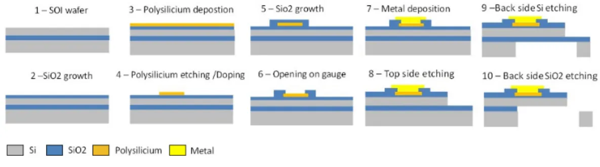
The fabrication process of silicon based sensors has been illustrated in Figure 1. 4-inch Silicon-on-insulator (SOI) wafers are taken as substrates applying a first thermal oxidation of 450 nm (1 and 2). The strain gauges are realized by depositing a layer of poly-silicon and patterned by photolithography and etching processes (3 and 4). A second thermal oxidation is carried out to ensure the dopant distribution through the polysilicon film and to isolate gages (5). Subsequently a metal layer (Ti/W-Au) is deposited and patterned that serves as contact (7) followed by a front side etching to shape the cantilever (8). Finally, a sacrificial layer is deposited in order to protect the structures and a back-side etching releases the cantilevers. Both etch steps (9 and 10) incorporate the deep reactive ion etching (DRIE) for silicon micromachining.
Fig. 1. Silicon cantilever fabrication process
2.2. Polycrystalline diamond micro-cantilever
The diamond micro-cantilever fabrication process shown in Figure 2 is based on a 4-inch single-side-polished silicon substrate. The substrate is thermally oxidized to create an insulating layer of 400 nm (1). The strain gauges are defined by depositing a layer of polysilicon (200 nm) and patterned by etching (2) in a similar fashion as for silicon sensors. A layer of tungsten has been deposited and patterned that serves as an etch stop layer for a later etching of diamond (3). The thickness of diamond cantilevers has been chosen such that they resonate at the same range of frequencies as silicon cantilevers of same length and width. Diamond is realized by dispersing a solution of diamond nano-particles (6 nm) in Poly-vinyl alcohol (PVA) and spin coated on the wafer surface (4) using the process described in [7]. This diamond surface layer is then exposed to a gas mixture of methane and hydrogen in a
Microwave Plasma Enhanced Chemical Vapor Deposition (MPECVD) based diamond growth reactor to synthesize diamond (5). An aluminum (Al) layer is sputter deposited and structured using photolithography that acts as a masking layer for cantilever shape and contact pads (6). Later on, diamond is etched away by DRIE (7) and the masking and etch-stop layers are chemically removed (8). The electrical contacts comprising 100 nm chromium (Cr) and 1000 nm gold (Au) are structured by standard photolithography and etching techniques (9). A similar Al masking layer finally releases the cantilevers by performing DRIE on the back side (10 and 11).
Fig. 2. Side view fabrication process for diamond cantilevers
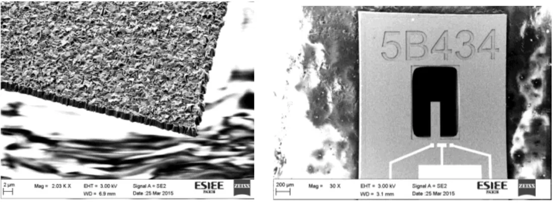
The grain size and morphology of the fabricated devices were verified using a scanning electron microscopy (SEM). The polycrystalline diamond film is uniform and continuous over the wafer and the average grain size is about 100 nm (Figure 3 (a)). Figure 3 (b) shows an optical micrograph of one micro-fabricated silicon cantilever.
Fig. 3. (a) SEM image of the board of a diamond cantilever; (b) SEM image of a silicon cantilever (top view) where we can see the identification code of the sensor
3. Methods
A set of ten cantilevers of different length (ranging from 260 μm to 650 μm) were chosen from both materials (silicon and diamond). Their exact dimensions in length and width were determined by scanning electron microscopy (SEM) and the thickness was measured by a surface profilometer. The samples were cleaned prior to the measurement and deposition of parylene layers and optimal deposition conditions were ensured in order to avoid the formation of droplets. The frequency profile (first mode) was measured using a laser vibrometer after each deposition. The measurement setup consists of a laser source emitting between 620 nm and 690 nm, an optical fiber interferometer OFV511, a demodulator OFV3001 (Polytec GmbH) and a network analyzer Agilent 89410A. It
1118 M. Possas et al. / Procedia Engineering 120 ( 2015 ) 1115 – 1119
allows to measure the mechanical oscillations of a microstructure by exploiting the Doppler Effect with high accuracy. The cantilevers are driven by a frequency sweep generated by a speaker.
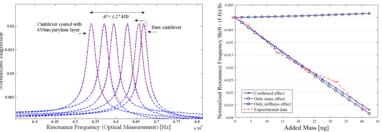
The parylene layer thickness was measured after each deposition and the equivalent added mass was computed. Each recorded frequency profile data was fitted using a three-parameter Lorentzian model in order to improve the estimation of resonance frequency and quality factor. A sample of the frequency response profiles and their fitting curves is depicted on Figure 4(a). The relative frequency shift due to the parylene deposition was compared to the theoretical calculations for 20 cantilevers and a sample of the analysis is shown in Figure 4(b).
Fig. 4. (a) Frequency response profiles obtained from optical measurements (blue) and their fitting curves (red) for repeated depositions; (b) Normalized Resonance Frequency Shift in dependence of added mass for theoretical mass effect only, theoretical stiffness effect only, theoretical
combined effect and experimental data for a 310μm length cantilever
4. Results and Discussion
In this paper we have reported the fabrication and characterization of silicon and diamond cantilever based sensors. For both materials, the resonance frequency measurement agrees with the theoretical expectations for cantilevers. Since the contribution of stiffness changes is not significant, the parylene layer can be modeled as an added mass. The experimental results have been found in accordance with the relative shift on frequency as shown in Figure 4(b).
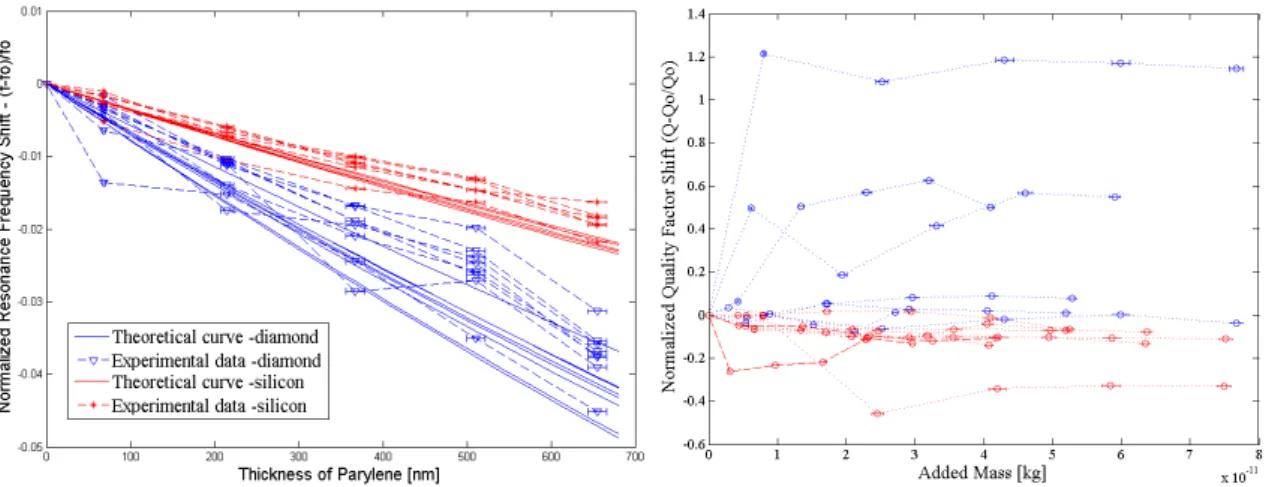
Fig. 5. (a) Frequency response profiles (blue) and their fitting curves (red) for repeated depositions of parylene on diamond and silicon cantilevers; (b) Normalized Resonance Frequency Shift in dependence of added mass for silicon and diamond cantilevers of same length.
The frequency shift has been compared for the cantilevers exhibiting similar resonance frequencies. As shown in Figure 5(a), the shift in resonance frequencies are 2.25 times higher in case of diamond cantilevers for the same amount of added mass. Figure 5(b) is the normalized frequency shift for silicon and diamond sensors computed from data presented on Figure 5(a).The amplitude of frequency response profiles depends on the relative position of the laser spot on the surface of the cantilever and hence the values have been normalized.
To generalize, diamond cantilevers are about three times more sensitive than silicon for any given geometry as depicted in Figure 6 (a). Figure 6 (b) shows the normalized quality factor shift due to an added mass. Quality factor of silicon sensors (red) are more affected by the adsorbed layer stiffness effect (negative shift) whereas diamond sensors quality factor (blue) increases with added mass effect (positive shift) since stiffness change effect is negligible for diamond sensors because of its high rigidity.
Fig. 6. (a) Normalized Resonance Frequency Shifts for diamond (blue) and silicon (red) sensors of different lengths – Theoretical curve and experimental data for each case; (b) Normalized Quality Factor Shifts for diamond (blue) and silicon (red) sensors of different lengths –
Experimental data for each case.
Acknowledgements
The authors would like to thank the European Community’s Seventh Framework Programme (FP7) under grant agreement n°285203 (SNIFFER PROJECT) for their financial support.
References
[1] Boisen, Anja, et al. "Cantilever-like micromechanical sensors." Reports on Progress in Physics 74.3 (2011): 036101.
[2] Chen, G. Y., et al. "Adsorptionϋinduced surface stress and its effects on resonance frequency of microcantilevers." Journal of Applied Physics 77.8 (1995): 3618-3622.
[3] Finot, Eric, Ali Passian, and Thomas Thundat. "Measurement of mechanical properties of cantilever shaped materials." Sensors 8.5 (2008): 3497-3541.
[4] Rasmussen, P. A., A. V. Grigorov, and Anja Boisen. "Double sided surface stress cantilever sensor." Journal of Micromechanics and Microengineering 15.5 (2005): 1088.
[5] Van Eysden, Cornelis A., and John E. Sader. "Resonant frequencies of a rectangular cantilever beam immersed in a fluid." Journal of applied physics 100.11 (2006): 114916.
[6] Possas, M., et al. “Fabrication and MicroMechanical Characterization of polycristalline diamond microcantilevers”, Design, Test, Integration & Packaging of MEMS/MOEMS, 2014.
[7] E. Scorsone, S. Saada, J.C. Arnault, P. Bergonzo, "Enhanced control of diamond nanoparticle seeding using a polymer matrix, " J. Appl. Phys., vol. 106, 014908, 2009.