HAL Id: hal-02428217
https://hal.archives-ouvertes.fr/hal-02428217
Submitted on 28 Feb 2020HAL is a multi-disciplinary open access archive for the deposit and dissemination of sci-entific research documents, whether they are pub-lished or not. The documents may come from teaching and research institutions in France or abroad, or from public or private research centers.
L’archive ouverte pluridisciplinaire HAL, est destinée au dépôt et à la diffusion de documents scientifiques de niveau recherche, publiés ou non, émanant des établissements d’enseignement et de recherche français ou étrangers, des laboratoires publics ou privés.
Resistive switching in a LaMnO 3 + δ /TiN memory cell
investigated by operando hard X-ray photoelectron
spectroscopy
Benjamin Meunier, Eugenie Martinez, Raquel Rodriguez-Lamas, Dolors Pla,
Mónica Burriel, Michel Boudard, Carmen Jimenez, Jean-Pascal Rueff, Olivier
Renault
To cite this version:
Benjamin Meunier, Eugenie Martinez, Raquel Rodriguez-Lamas, Dolors Pla, Mónica Burriel, et al.. Resistive switching in a LaMnO 3 + δ /TiN memory cell investigated by operando hard X-ray pho-toelectron spectroscopy. Journal of Applied Physics, American Institute of Physics, 2019, 126 (22), pp.225302. �10.1063/1.5125420�. �hal-02428217�
1
Resistive switching in a LaMnO
3+/TiN memory cell investigated by
operando hard X-ray photoelectron spectroscopy
Benjamin Meunier1, Eugénie Martinez2, Raquel Rodriguez-Lamas1, Dolors Pla1, Monica Burriel1,
Michel Boudard1, Carmen Jimenez1, Jean-Pascal Rueff3,4, Olivier Renault2
1Univ. Grenoble Alpes, CNRS, Grenoble INP*, LMGP, F-38000 Grenoble, France
* Institute of Engineering Univ. Grenoble Alpes
2Univ. Grenoble Alpes, CEA, LETI, 38000 Grenoble, France
3Synchrotron-SOLEIL, BP 48, Saint-Aubin, F-91192 Gif-sur-Yvette, France
4Sorbonne Université, CNRS, Laboratoire de Chimie Physique - Matière et Rayonnement
(LCPMR), F-75005 Paris, France
ABSTRACT
Transition metal oxides are promising candidates in the development of valence change memories
thanks to their ability to present valence change mechanism. The resistive switching mechanism of
TiN/LaMnO3+/Pt devices was investigated by operando hard X-ray photoelectron spectroscopy after
careful in situ electrical characterization. The results presented here highlight the oxygen exchange
process at the TiN/LMO interface. The active TiN top electrode acts as an oxygen getter, pumping
O2- anions which are attracted by the positive bias and repelling them under negative bias. This drift
of charged defects is correlated with variations of the interfacial resistance. Our results confirm the
critical role of the TiN/LMO interface as well as of oxygen drift in the resistive switching behaviour
2
Motivated by the growing interest in novel non-volatile resistive random-access memories (RRAMs),
many new oxide-based heterostructures have emerged as potential candidates to build alternative
memristive devices. Among the plethora of oxides exhibiting valence change mechanism, a number
of perovskites, such as (Pr,Ca)MnO3,[1] SmNiO3,[2] SrZrO3,[3-5] LaSrMnO3,[6] as well as the
thoroughly-studied SrTiO3[7] have shown memristive behavior. Despite their promising functional
properties (high speed, large ON/OFF ratio, large programming window, high endurance),
fundamental knowledge and a thorough understanding of the RS mechanisms involved are in most
cases still rather scarce. This is due to the difficulty to get element-specific information from the
resistive material in an operating device.
The non-stoichiometric transition metal oxide LaMnO3+ (LMO) shows a resistive switching behavior
which was shown to be governed by the oxygen vacancy content of the material.[8,9] The apparent
oxygen excess in LMO is ascribed to the formation of La and/or Mn cation vacancy sites (i.e. La
1-x□x,Mn1-y□yO3, viz. LaMnO3+), where □ represents cation vacancies andcharge neutrality remains
fulfilled thanks to the coexistence of Mn3+/Mn4+ oxidation states.[10-13] Therefore, the valence state of
the material is strongly correlated to the oxygen content and Mn4+ can be seen as a dopant.[14]
We recently investigated the microscopic mechanisms of local interfacial RS in LaMnO3+ by
conductive atomic force microscopy (c-AFM)[15] and highlighted that the change in resistance is
associated with a drift of oxygen ions to the surface and the concomitant variation in the Mn valence
state, which results in modifications in the transport mechanism. However, the configuration used
presents several specificities (e.g. low current density, bare surface, large active area …) that do not
match the requirements of a standard functional device. Thus, to go a step further in the understanding
of the memristive behavior of LMO-based cells, we have now tested more realistic operating devices,
in which the active oxide layer is sandwiched between a top- and a bottom-electrode.
Hard x-ray photoelectron spectroscopy (HAXPES) has shown excellent capabilities for
non-destructive operando characterization of functional devices.[16-18] Indeed, compared to conventional
3
synchrotron radiation (2.4 – 12 keV) gives information from a region up to 5 times deeper inside the
sample and even deeper using inelastic background analysis.[19,20] HAXPES has been successfully
implemented during resistive switching operation to study buried interfaces of different oxide-based
heterostructures such as Ti/HfOx,[21-26] TiN/Hf0.5Zr0.5O2,[27] Pt/Ti/Pr0.5Ca0.5MnO3,[22]
Au/FeSTO/NbSTO,[28] and TiN/Pt/NiO.[29] Real operando measurements, consisting in biasing the
device while performing HAXPES, are therefore enlightening in order to understand the changes in
elemental composition and charge distribution inside the device. Such a method was previously used
for studying interface polarization in piezoelectric oxide-based high-density capacitors.[30]
In the present contribution, we study the case of LMO memristive devices grown on platinized silicon
and covered by TiN, a technologically-relevant top electrode. Operando HAXPES measurements
were performed at different resistance states, carefully induced by in situ electrical characterization.
The results reveal the chemical modifications and reactions occurring at the LMO/TiN interface.
In order to match the HAXPES requirements, the TiN electrode should be thin enough to allow the
photoelectrons passing through and the remote electrical contacts should be employed to avoid any
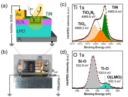
obstruction of the active area. The resulting design is presented in Figure 1 (a). The LMO thin film
(100 nm-thick, grown following strategy III of Ref.[31]) is partially covered by a 50 nm thick Si3N4
insulating layer deposited by sputtering (CT100 Alliance Concept). The structural characterization of
the LMO film (XRD and Raman spectroscopy) exhibiting the coexistence of both rhombohedral and
orthorhombic phases can be found in Figure S2 of the Supporting Information. 100x100 m² squared craters were etched through the Si3N4 layer and subsequently covered by a TiN layer of
approximately 6 nm thick also deposited by sputtering. In this way, the HAXPES measurements were
carried out on well-defined regions of interest of 100×100 m² comprising the top TiN top electrode and the LMO surface below, simultaneously achieving the electrical biasing of the sample. 100
4
electrode and allowing the wire bonding to the sample holder. As shown in Figure 1(b) the sample
holder is a printed circuit board hosting several electrodes. The grounded electrode (left of the image)
is bonded to the Pt bottom electrode, while the four top electrodes (right of the image) are
wire-bonded to the top Au/TiN electrodes and each of them can be independently connected to a
sourcemeter (Keithley 2635B). Due to the large distance between the sample in the HAXPES
chamber and the operator, the wire resistance and multiple contacts resistance cannot be neglected.
The difference between the resistance measured directly at the sample’s output and the resistance
once the sample is mounted and placed in the HAXPES chamber give a total external resistance of
2.9 .
The HAXPES experiments were performed at the Galaxies beamline, SOLEIL synchrotron facility
(St-Aubin, France). The pressure in the analysis chamber remained around 10-8-10-7 mbar during the
whole experiment. The photon energy was set to 7994.51 eV (as determined from the Fermi level of
the Au top electrode at zero bias) with a take-off angle of 50°. The incident photon energy was selected
with a Si(333) double crystal monochromator, and the photons were focused to a 30×80 µm2 beam
spot using a toroidal mirror. The photon and analyzer bandwidths were both set to 150 meV providing
an overall energy resolution of 210 meV. The Au 4f, Ti 1s and O 1s core-levels were recorded after
each change in resistance, while still biasing the sample. The La 3d core-level could not be recorded
due to the poor signal-to-noise ratio and the large energy range required, while the manganese
core-levels were not analyzed because of intrinsically low cross-sections and severe overlapping with the
Au photoemission lines. A Shirley-type background was subtracted from all the spectra. The inelastic
mean free path estimated for the different core levels through the LMO/TiN stack provides an average
sampling depth of 25 nm.[32]
The initial spectra (at 0 V and initial resistance state - IRS) of Ti 1s and O 1s are shown in Figure 2(c)
and (d). Peak fitting was performed using a pseudo-Voigt function with 70% and 20 % of Lorentzian
peak for Ti 1s and O 1s respectively. The Ti 1s photoemission spectrum consists of three contributions.
5
contributions are attributed to TiOxNy (4966.6 eV) and TiOx (4968.2 eV) resulting from the oxidation
of TiN.[33,34] The larger width of the oxide peaks (FWHM = 2.6 eV) compared to the TiN peak
(FWHM = 1.3 eV) is attributed to inhomogeneities in the oxides composition. The composition of
the top as-deposited electrode has been calculated to be of 32% TiN and 68% of oxides (26% TiOxNy
and 42% TiOx). Even if the fully oxidized TiOx is more likely to be found on the surface and TiOxNy
at the interface, these considerations are not fully accurate regarding the low thickness of the top
electrode.
The O 1s spectrum in Figure 2(d) is dominated by the SiO2 contribution coming from the Si3N4
oxidized surface due to the large footprint of the incident beam on the surface. Two other contributions
are identified at 530.6 eV and 530.3 eV assigned to Ti-O bonds (from TiOx and TiOxNy) and to LMO,
respectively. A more complete HAXPES characterization of the sample (presenting La 3d3/2, Mn 3s,
O 1s and N 1s in different regions) can be found in Figure S3 of Supporting Information.
Figure 1 (a) sample description (b) picture of a mounted sample (c)(d)HAXPES spectra of Ti 1s
6
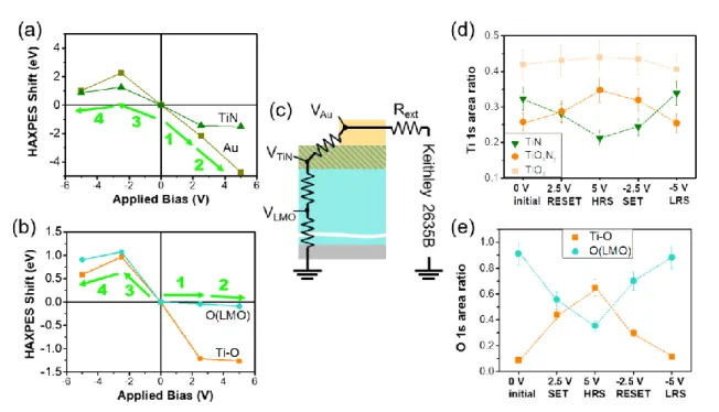
We now address the results of the operando measurements of the LMO/TiN memory cell. The Au 4f,
O 1s and Ti 1s core-levels were recorded while biasing the device with different voltages following
the sequence: 0 V → 2.5 V → 5V → -2.5V → -5V → 0V. The core level spectra for each step are
presented in the Supporting Information (Au 4f in Figure S4, Ti 1s in Figure S5 and O 1s in Figure
S6). It should be notice that the -5V and final 0V spectra are similar shape which exclude the presence
of potential volatile effects due to the presence of the electric field. During this sequence, the sample
resistance changes from the initial resistance state (R= 6.2 ) to the HRS (R= 52 ) at +5 V and back to a LRS (R=12 ) at -5 V.
Figure 2(a) and (b) show the peak shifts, relative to 0 bias, of Au 4f, Ti 1s(TiN), O 1s(LMO) and O
1s(Ti-O) for different applied voltages and resistance states. When a bias is applied, the energy levels
will drift away from the Fermi level and the measured kinetic energy of electrons will be shifted. The
energy shift of an element corresponds to the voltage “seen” at the location of this element in the
device. Thus, as depicted in Figure 3(b) the deeper the layer, the smaller the corresponding HAXPES
shift (i.e. VAu > VTiN > VLMO). The voltage applied to the device is progressively lost in the series
resistances corresponding to each material or interface of the stack. Considering the Au 4f peak from
the top electrode, the total resistance (Rtot=Rdev+Rext) of the device (Rdev = RLMO+RTiN+RAu) and the
external resistance (Vappl – VAu = I.Rext) can be calculated with the following potential divider
relationship:
𝑅𝑡𝑜𝑡 = 𝑅𝑒𝑥𝑡. (1 + 𝑉𝐴𝑢 𝑉𝑎𝑝𝑝𝑙− 𝑉𝐴𝑢)
being Rext = 2.9 the external resistance and Vappl the applied voltage. Therefore, for Vappl = +5 V,
the Au 4f energy shift yields VAu = 4.73 V and the total resistance drop can be calculated to be Rtot =
53.7 , meaning that the device is in HRS. Similarly, for Vappl = -5 V, VAu = -1.0 V and Rtot = 3.6 ,
corresponding to the LRS case. These resistance values are comparable with those experimentally
measured with the Keithley during the HAXPES measurement (RHRS = 52 and RLRS = 12 ), the
7
reliability of the experimental set-up and the relevance of the spectroscopic measurements in a
specific resistance state of the device. When switching the device to HRS, i.e. when applying a
positive bias (2.5 and 5 V), a potential drop is observed between the TiN and LMO layers and between
the TiN and Au electrode. During the RESET event (IRS to HRS) voltage difference between each
layer increase, first between TiN and LMO at 2.5 V and then between TiN and Au. During the SET
event (HRS to LRS) at -2.5 V the potential drop between TiN and LMO strongly decreases (i.e. VTiN
-VLMO ~ 0 V) to almost reach the same voltage.
Figure 2. (a) HAXPES shift of Au 4f, Ti 1s and (b) O 1s depending on the applied voltage (c)
equivalent circuit of the structure with Rext = 2.9 (d) relative areas of all Ti 1s and (e) O 1s
contributions depending on the applied bias and the resistance state
Figure 2(c) shows the evolution of all Ti components after normalization of their area by the total Ti
1s area (which is assumed to be constant). During the RESET event (from 0 V to 5 V), the Ti 1s area
from TiN decreases while the oxide contributions increase indicating the oxidation of the positively
biased TiN electrode. Similar behavior of the Ti-O is observed in the O 1s spectra in Figure S5 as
well as a decrease of the O(LMO) contribution. Comparing each of the Ti oxide, the TiOxNy (partially
8
42% to 44%. This is indicative of the partial oxidation of the TiN electrode, remaining moderate
during the RESET event. This oxygen drift from the LMO to the top electrode, in the form of O
2-anions, is driven by the electric field. Conversely, during the SET event (applying -2.5 and -5 V),
each contribution goes back to a value close to its initial value. A reversed oxygen drift, from TiOxNy
back into the LMO is observed driven by the electric field.
The consequence of this redox reaction at the interfacial TiOxNy layer is the increase/decrease of the
potential drop previously observed at this interface. The exchange of oxygen ions between LMO and
the TiN electrode is described in Figure 3.
Figure 3. Sketch of the proposed oxygen exchange process occurring during RESET ( VSET > 0) and
SET (VRESET < 0). Inserts: the nominal composition of the TiN electrode based on the quantification
of the Ti 1s area ratios shown in Figure3(c).
In this work we presented operando HAXPES measurements for investigating the resistive switching
mechanisms taking place in a TiN/LMO/Pt memory cell under application of electrical bias. The use
of HAXPES has successfully demonstrated its ability to observe buried interfaces and fingerprint
relevant modifications occurring during resistive switching. In particular, spectra recorded during the
process reveal changes in the composition of both the TiN electrode and the LMO itself. Fitting of
the Ti 1s spectra (and confirmed by the O 1s spectra) clearly indicates a partial oxidation of the TiN
9
The mechanism can be described by a redox reaction triggered by the oxygen drift at the TiN/LMO
interface due to the external bias. The TiOxNy interlayer plays the role of an oxygen getter during
RESET, expelling oxygen back in LMO during the SET process. Thanks to careful operando
spectroscopic analysis, we proposed a redox model to fully describe the physiochemical mechanism
occurring in a potential technologically-relevant memory cell consisting in a LaMnO3+ active layer
and a TiN top electrode.
SUPPORTING INFORMATION
See supporting information for more complete sample characterization and further detailed
HAXPES spectra.
ACKNOWLEDGMENTS
This work has been supported by the ANR funded project “Alps Memories”
(ANR-15-CE24-0018). We acknowledge SOLEIL for provision of synchrotron radiation facilities (Proposal No.
20170169). The authors want to thank Odette Chaix-Pluchery and Hervé Roussel for Raman and
X-ray diffraction measurements. Sample fabrication has been performed with the help of the
“Plateforme Technologique Amont” of Grenoble with the financial support of the CNRS Renatech
network. In addition, this work benefited from the facilities and expertise of the OPE)N(RA
characterization platform of FMNT (FR 2542, fmnt.fr) supported by CNRS, Grenoble INP and UGA.
REFERENCES
[1] D. S. Kim, Y. H. Kim, C. E. Lee, Y. T. Kim, Phys. Rev. B 2006, 74, 174430.
[2] J. Shi, S. D. Ha, Y. Zhou, F. Schoofs, S. Ramanathan, Nat. Commun. 2013, 4, 2676.
[3] L. Weston, A. Janotti, X. Y. Cui, B. Himmetoglu, C. Stampfl, C.G. Van de Walle, Phys. Rev.
B 2015, 92, 085201.
[4] D. S. Kim, C. E. Lee, Y. H. Kim, Y. Y. Kim, J. Appl. Phys. 2006, 100(9), 0-4.
10
[6] J. C. Gonzalez-Rosillo, R. Ortega-Hernandez, J. Jareño-Cerulla, E. Miranda, J. Suñe, X.
Granados, X. Obradors, A. Palau, T. Puig, J. Elecrtoceram. 2017, 39, 185. [7] K. Szot, W. Speier, G. Bihlmayer, R. Waser, Nat. Mater. 2006, 5, 312-320.
[8] Y.-L. Jin, Z.-T. Xu, K.-J. Jin, C. Ge, H.B. Lu, G.-Z. Yang, Mod. Phys. Lett. B 2013, 27(11),
1350074.
[9] Z.-T. Xu, K.-J. Jin, L. Gu, Y.-L. Jin, C. Ge, C. Wang, H.-Z. Guo, H.-B. Lu, R.-Q. Zhao, G.-Z. Yang,
Small 2012, 8, 1279-1284.
[10] J. Töpfer, J. B. Goodenough, J. Solid State Chem. 1997, 130, 117-128.
[11] B. C. Tofield, W. R. Scott, J. Solid State Chem. 1974, 10, 183-194.
[12] J. A. M. van Roosmalen, E. H. P. Cordfunke, J. Solid State Chem. 1994, 110, 106-108.
[13] J. A. M. van Roosmalen, P. van Vlaanderen, E. H. P. Cordfunke, J. Solid State Chem. 1995,
114, 516-523.
[14] S. Badgevicius, K. Maas, M. Boudard, M. Burriel, J. Electroceram. 2017, 39, 157.
[15] B. Meunier, D. Pla, R. Rodriguez-Lamas, M. Boudard, O. Chaix-Pluchery, E. Martinez, N.
Chevalier, C. Jiménez, M. Burriel, O. Renault, ACS Appl. Electron. Mater. 2019, 1, 5, 675-683.
[16] F. Borgatti, F. Offi, P. Torelli, G. Monaco, G. Panaccione, J. Electron. Spectrosc. 2013, 190,
228-234.
[17] D. Céolin, J. M. Ablett, D. Prieur, T. Moreno, J.-P. Rueff, T. Marchenko, L. Journel, R.
Guillemin, B. Pilette, T. Marin, M. Simon, J. Electron. Spectrosc. 2013, 190, 188-192.
[18] J. Rubio-Zuazo, G. R. Castro, J. Electron. Spectrosc. 2013, 190, 205-209.
[19] S. Tougaard, Surf. Interface Anal. 1998, 26(4), 249-269.
[20] S. Tougaard, J. Electron. Spectrosc. Relat. Phenom. 2010, 178-179, 128-153.
[21] T. Bertaud, M. Sowinska, D. Walczyk, S. Thiess, A. Gloskovskii, C. Walczyk, T. Shroeder, Appl.
Phys. Lett. 2012, 101, 143501.
[22] F. Borgatti, C. Park, A. Herpers, F. Offi, R. Egoavil, Y. Yamashita, A. Yang, M. Kobata, K. Kobayashi, J. Verbeek, G. Panaccione, R. Dittmann, Nanoscale 2013, 5, 3954.
11
[23] Y. S. Lin, F. Zeng, S. G. Tang, H. Y. Liu, C. Chen, S. Gao, Y. G. Wang, F. Pan, J. Appl.
Phys. 2013, 113, 164510.
[24] S. U. Sharath, T. Bertaud, J. Kurian, E. Hildebrandt, C. Walczyk, P. Calka, P. Zaumseil, M.
Sowinska, D. Walczyk, A. Gloskovskii, T. Schroeder, L. Alff, Appl. Phys. Lett. 2014, 104,
063502.
[25] M. Sowinska, T. Bertaud, D. Walczyk, S. Thiess, M. A. Schubert, Appl. Phys. Lett. 2012,
100, 233509.
[26] M. Sowinska, T. Bertaud, D. Walczyk, S. Thiess, P. Calka, L. Alff, C. Walczyk, T.
Schroeder, J. Appl. Phys. 2014, 115, 204509.
[27] Y. Matveyev, D. Negrov, A. Chernikova, Y. Lebedinskii, R. Kirtaev, S. Zarubin, E.
Suvorova, A. Gloskovskii, A. Zenkevich, ACS Appl. Mater. Interfaces 2017, 9, 43370-43376.
[28] C. Lenser, A. Koehl, I. Slipukhina, H. Du, M. Patt, V. Feyer, C. M. Schneider, M. Lezaic,
R. Waser, R. Dittmann, Adv. Funct. Mater. 2015, 25, 6360-6368.
[29] P. Calka, E. Martinez, D. Lafond, S. Minoret, S. Tirano, B. Detlefs, J. Roy, J. Zegenhagen,
C. Guedj, J. Appl. Phys. 2011, 109, 124507.
[30] I. Gueye, G. Le Rhum, O. Renault, D. Cooper, D. Ceolin, J.-P. Rueff, N. Barrett, Appl.
Phys. Lett. 2017, 11(3), 032906.
[31] R. Rodriguez-Lamas, D. Pla, O. Chaix-Pluchery, B. Meunier, F. Wilhelm, A. Rogalev, L.
Rapenne, X. Mescot, Q. Rafhay, H. Roussel, M. Boudard, C. Jiménez, M. Burriel, Beilstein J.
Nanotech. 2018, 10, 389-398.
[32] H. Shinotsuka, S. Tanuma, C. J. Powell, and D. R. Penn, Surf. Interface Anal. 47, 871
(2015).
[33] O. Renault, E. Martinez, C. Zborowski, J. Mann, R. Inoue, J. Newman, K. Watanabe, Surf.
Interface Anal. 2018,1-5.
[34] P. Risterucci, O. Renault, C. Zborowski, D. Bertrand, E. Torres, J.-P. Rueff, D. Ceolin, G.