Publisher’s version / Version de l'éditeur:
Vous avez des questions? Nous pouvons vous aider. Pour communiquer directement avec un auteur, consultez la première page de la revue dans laquelle son article a été publié afin de trouver ses coordonnées. Si vous n’arrivez pas à les repérer, communiquez avec nous à [email protected].
Questions? Contact the NRC Publications Archive team at
[email protected]. If you wish to email the authors directly, please see the first page of the publication for their contact information.
https://publications-cnrc.canada.ca/fra/droits
L’accès à ce site Web et l’utilisation de son contenu sont assujettis aux conditions présentées dans le site LISEZ CES CONDITIONS ATTENTIVEMENT AVANT D’UTILISER CE SITE WEB.
[OSF Preprints], 2018-10-31
READ THESE TERMS AND CONDITIONS CAREFULLY BEFORE USING THIS WEBSITE.
https://nrc-publications.canada.ca/eng/copyright
NRC Publications Archive Record / Notice des Archives des publications du CNRC :
https://nrc-publications.canada.ca/eng/view/object/?id=6a483855-200c-45f0-a5df-1f7238ddaf9b https://publications-cnrc.canada.ca/fra/voir/objet/?id=6a483855-200c-45f0-a5df-1f7238ddaf9b
NRC Publications Archive
Archives des publications du CNRC
This publication could be one of several versions: author’s original, accepted manuscript or the publisher’s version. / La version de cette publication peut être l’une des suivantes : la version prépublication de l’auteur, la version acceptée du manuscrit ou la version de l’éditeur.
Access and use of this website and the material on it are subject to the Terms and Conditions set forth at
Mapping the global design space of integrated photonic components
using machine learning pattern recognition
Melati, Daniele; Grinberg, Yuri; Janz, Siegfried; Cheben, Pavel; Schmid,
Jens H.; Sánchez-Postigo, Alejandro; Xu, Dan-Xia
1
Mapping the global design space of integrated
photonic components using machine learning
pattern recognition
Daniele Melati
1,†, Yuri Grinberg
2,†, Siegfried Janz
1, Pavel Cheben
1,
Jens H. Schmid
1, Alejandro Sánchez-Postigo
3and Dan-Xia Xu
1,* 1Advanced Electronics and Photonics Research Centre, National Research Council Canada, 1200 Montreal Rd., Ottawa, ON K1A 0R6, Canada
2
Digital Technologies Research Centre, National Research Council Canada, 1200 Montreal Rd., Ottawa, ON K1A 0R6, Canada
3
Universidad de Málaga, Departamento de Ingeniería de Comunicaciones, ETSI Telecomunicación, Campus de Teatinos s/n, 29071 Málaga, Spain
*e-mail: [email protected]
†These authors contributed equally to this work.
Abstract
Integrated photonic devices are at the basis of modern optical communications but their design remains a time-consuming and mostly iterative process. Recent design methods employing optimization algorithms
make it possible to simultaneously optimize a large number of parameters and generate non-trivial geometries and novel functionalities. However, these approaches give little insight on the influence of the
design variables on device performance, nor address the possibility of degenerate designs with similar performance. Using machine learning methods, we demonstrate through the design of a vertical grating
coupler that a large number of degenerate designs with regard to the primary objective (coupling efficiency) exist, but they have distinct properties in other performance criteria. Pattern recognition reveals the relationship between these designs and reduces the characterising variables from the original five to two. This finding enables the exhaustive yet efficient coverage of the design space, being mapped
onto a 2-dimensional hyperplane. The interplay of the design parameters and multiple performance criteria then can be clearly visualized with a vastly reduced computational effort, allowing the designer to
understand and balance competing design requirements. We believe this is the first time such a global perspective is presented for high dimensional design problems in integrated photonics, representing a
2
Integrated photonic components perform complex optical functions that underlie modern optical communication networks and also have wide ranging applications in computing, automation, sensing and life sciences1,2. Despite the growing interest and use, photonic component design has largely remained a time-consuming process that relies on theoretical knowledge and physical intuition. For a desired functionality, an initial design is proposed according to particular physical concepts. The performance is evaluated semi-analytically or numerically, and typically optimized through a repetitive process of modifying a small set of parameters in a sequential manner. At the same time, novel photonic devices that employ increasingly complex geometries and metamaterials are continuously proposed3–5. In these scenarios, not only do the number of design parameters vastly increase but they are often strongly interrelated. Sequential optimization is no longer applicable and simultaneous optimization of multiple variables is required. Optimization tools such as the genetic algorithm6–8, particle swarm9,10, and gradient-based optimization11–14 are increasingly used to search more efficiently for high-performance designs15. Inverse design methods have been proposed to tackle this challenges, demonstrating highly compact devices employing non-intuitive structures16–21. More recently, supervised machine learning methods such as the artificial neural network have begun to enter the fray in speeding up the search process22,23. While all these approaches represent significant improvement to the design flow, the resulting process still only leads to isolated designs optimized for a single primary performance criterion. This offers little physical insight on the influence and inter-dependence of the design parameters in determining the device performance. Although it is tacitly recognized that there may be other designs offering similar performance in terms of the primary criterion (i.e. degenerate designs), a practical methodology for generating all suitable device candidates does not yet exist. Consequently, careful balancing of different performance considerations – an indispensable task prior to fabrication, integration and system design – becomes difficult. A global perspective on the design space of such photonic devices is missing.
We propose here that a suite of machine learning (ML) tools now widely available, including global optimization, supervised learning and unsupervised ML pattern recognition, can be applied to this purpose. Our objective is to create a methodology for building a global map of a multi-parameter design space while using a tractable amount of time and computational resources. This goal is fundamentally different from the current search-based methods targeting a single optimal design.
As a first demonstration-of-concept, we analyze a vertical grating coupler in the silicon-on-insulator (SOI) platform. Grating couplers are a convenient way to couple light between an integrated photonic circuit and an optical fiber. To suppress the second order diffraction, gratings are typically designed to diffract light at an angle from the surface normal24. However, perfectly vertical emission is desirable as it would allow simpler packaging, and various designs have been proposed in the literature14,25–29. A recent design, optimized using particle swarm optimization, has been reported by Watanabe et al.10 and provides a good fiber-chip coupling efficiency and a fairly low level of back-reflections. This design consists of five subwavelength segments in each period that need to be simultaneously optimized and therefore provides a good target to demonstrate the potentiality of a machine-learning-based design approach. Applying a number of ML techniques, we discover that a large number of designs with state-of-the-art fiber coupling efficiency exist, and to a good approximation they all lie on a two-dimensional hyperplane, i.e. they can be described using only two relevant parameters instead of the original five. This discovery opens the possibility of an exhaustive mapping of the sub-space of good designs by scanning through this hyperplane as well as its orthogonal planes. The outcome of such scans provides a clear description of the
3
device behavior in terms of coupling efficiency, reflection and sensitivity to dimensional variations. Together, these results provide a comprehensive picture that enables informed decision-making based on the relative priorities of all relevant performance specifications and figures-of-merits for a particular application. To the best of our knowledge, this is the first time such a global perspective is obtained by leveraging unsupervised machine learning techniques for high dimensional design problems in integrated photonics
Strategy for characterizing a multi-parameter design space
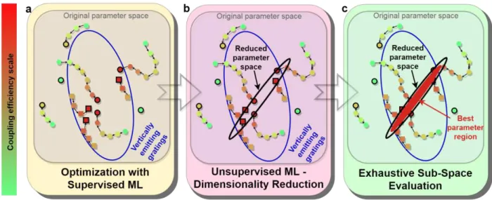
Dealing with the design of multi-parameter devices commonly requires giving up the opportunity to obtain extensive information on the large parameter space due to constrains on computational resources. We tackle this problem by introducing a three-stage process. In the first stage we generate a sparse collection of devices (i.e. isolated points in the parameter space) all meeting a selected performance criterion. In the second stage we apply an unsupervised pattern recognition technique to analyse the relationship between these degenerate designs and explore whether a lower dimensional sub-space can be found to include all good design solutions meeting the performance criterion. In the last stage we perform a global mapping of the properties of the designs in this sub-space including additional performance metrics.
Fig. 1 A three-stage approach for the characterization of the vertical grating coupler design space. a Global optimization (here, random restart followed by local search) is used to find a small collection of devices with high fiber coupling efficiency, depicted as dark red circles. A trained machine learning predictor is used in conjunction with the global optimizer to speed-up the search by quickly providing grating design candidates with nearly vertical emission as starting points for the optimizer (depicted as red squares). b Dimensionality reduction (principal component analysis) is employed to reveal the reduced parameter space of the designs with good performance, characterized by a low-dimensional hyperplane as depicted by the black contour. c Devices belonging to the reduced parameter space can be exhaustively evaluated with respect to different performance criteria (dark red area).
4
A vertical grating coupler with five segments per period is taken as the study case10. As shown in Fig. 1a, global optimization is used to search for a set of designs with state-of-the-art fiber coupling efficiency. A supervised machine learning predictor is also trained to predict the diffraction angle of this relatively complex structure, speeding up the search process. Such a predictor has the potential of being applied also to other performance criteria. For the second and key step, principal component analysis30 (PCA) is used (Fig. 1b) to analyze the relationship between the designs found in stage 1. PCA is an unsupervised machine learning patter recognition technique that has been used widely and successfully across various engineering and science disciplines31–34 and is implemented in most scientific computing platforms (e.g. Matlab, R, etc.). It finds a sequence of best linear approximations to the dataset (based on minimizing the least squared errors) and the results explicitly show how many orthogonal linear projections are needed to represent the dataset within a certain level of accuracy. If a lower dimensional sub-space is found and
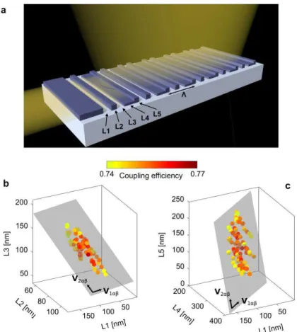
Fig. 2 a Schematic representation of the grating coupler structure. The guided light is vertically diffracted by a grating realized periodically interleaving a pillar of height 220 nm and an L-shaped section partially etched to 110 nm. The blazing effect of the L-shape ensures a high vertical directionality while the pillars are designed to suppress back-reflections by destructive interference. The five design parameters L1-L5 defines the original five-dimensional parameter space and the grating period Λ. b,
c The procedure depicted in Fig.1a allows to find many high performance designs with a fiber coupling efficiency larger than 0.74. Pictures show two three-dimensional projections of the five-dimensional parameter space. Dots represent the designs (L1-L5
values) with the associated coupling efficiency encoded by different colours. These designs are approximately contained in a well-defined area of a hyperplane (reduced parameter space) discovered through a principal component analysis. The three-dimensional projections of the reduced parameter space are shown in gray. The hyperplane is defined by the two vectors V1αβ and
5
validated to contain all good designs, the rest of the design space can be excluded from further investigation. We complete the investigation by performing an exhaustive evaluation of coupling efficiency, back-reflections and fabrication tolerance for all the designs included in the lower-dimensional sub-space, as shown in Fig. 1c.
Discovery of comparable high-performance vertical grating designs
The considered grating structure is illustrated in Fig. 2a. Each period of the grating consists of a pillar of 220 nm in height and an L-shaped section partially etched to 110 nm10. The L-shape approximates the angled facet of a conventional blazed grating14 in a way that can be fabricated with standard lithography and etch methods. This blazing ensures that light is primarily diffracted upwards. The silicon pillars are used to suppress back-reflections by destructive interference. The structure dimensions (L1 … L5) define the five-dimensional design parameter space we explore in this work.
As primary optimization objective we choose the coupling efficiency η of the diffracted TE-polarized light to a standard single mode optical fibre (SMF-28) placed vertically on top of the grating. Low back-reflection is another important consideration in minimizing the impact of the grating to other upstream components in the system. These considerations lead to the formulation of the optimization problem for the first stage represented in Fig. 1a as:
maximize�
1⋯�5 � ⋯ �5 subject to � � ⋯ �5 < − �
nm < Λ < μm; ��> nm, � = ⋯ .
These conditions maximize the coupling efficiency η and constrain the back-reflections r to be smaller than a defined threshold (-15 dB in this case). Additional constraints on the grating period Λ and the minimum feature size are included to confine the optimization to designs that are physically manufacturable using state-of-the-art silicon photonics fabrication processes. The wavelength of light is set at = 1550 nm. A highly-efficient Fourier-type 2-D eigenmode expansion simulator35 is used to compute the device performance. For additional computational details and description of the optimization algorithm, please refer to the section Methods.
The optimization stage is halted after we obtain 45 good designs, defined here as gratings with coupling efficiency η greater than 0.74 and back-reflection less than -15 dB. These solutions are represented by the points in the five-dimensional parameter space [L1 … L5] shown in Figs. 2b and 2c through two 3-D projections, with the corresponding coupling efficiency encoded by the color of the markers. The visualizations suggest that good designs follow a certain pattern in the 5-D space that we attempt to learn in the next stage.
6
Sub-space identification through dimensionality reduction
In this key stage we exploit PCA to study the relationship between the sparse set of solutions obtained solving the optimization problem (1). When PCA is applied to the pool of 45 good grating designs, two principal components are found to be sufficient to accurately represent the entire pool. That is, all good designs approximately lie on a 2-D hyperplane – the reduced parameter space – defined by the vectors
V1αβ = [-0.043, 0.378, -2.082, 4.477, -3.021] and V2αβ = [-2.580, 1.081, -3.769, -0.386, 2.193]. The vector components are expressed in nanometers. The points belonging to this hyperplane can thus be written as �� = �� + �� + � (2)
where the components of the vector Lk are the five dimensions Li,k for the k-th design and Cαβ = [102,73,156, 243,156] is a constant vector that defines the reference origin on the hyperplane. Two scalar coefficients αk and βk are thus sufficient to completely describe the k-th design. The 2-D reduced parameter space (hyperplane) discovered by PCA is shown in Figs. 2b and 2c in gray on the same projections used to represent the 45 good designs.
To quantify the “difference” between two different designs A and B, we use the Manhattan distance defined as ∑5�= |��, − ��, |. The error incurred by approximating the original sparse set of 45 good designs with the nearest corresponding design on the 2-D hyperplane in terms of the Manhattan distance is below 6 nm on average, with the worst case being below 12 nm. About the same average error is obtained if we randomly choose 5 designs as a basis for generating another hyperplane using the PCA analysis and then calculate the approximation error of the other 40 designs. Furthermore, a PCA-based approximation of 45 designs to 1-D incurs an average error of more than 50 nm, while a 3-D approximation incurs an average error of 3 nm. This warrants our choice of 2-D approximation as the error reduction by adding the second dimension is significant, while further addition of a third dimension leads to a very small improvement.
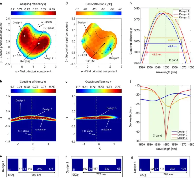
We validate the PCA outcome by verifying that the projection on the reduced parameter space (the α-β hyperplane) is a sufficient representation of the entire sub-space of good gratings. First, we generate a uniform grid covering the α-β hyperplane. For each point [αk, βk] we obtain the corresponding point [L1,k … L5,k] in the original parameter space through equation (2) and compute the coupling efficiency η. The
results are shown in Fig. 3a only for the designs with η > 0.7. Note that not all points on the α-β plane provide high coupling efficiency. A unit change in α or β corresponds to a Manhattan distance of 100 nm. A large region of good designs with η > 0.74 is enclosed by the black solid line. Remarkably, although all the good designs have similar coupling efficiencies ranging from = 0.74 to η = 0.76, the actual structure of the gratings can vary quite significantly, as discussed in detail in the next section. Without dimensionality reduction, there is no obvious way to identify a pattern that all good designs follow. As a further verification we generate two additional 2-D hyperplanes Γ-Π and X-Π that are orthogonal to each other and to the β plane. They provide two different “cuts” through the reduced parameter space α-β and their projections are shown in Fig. 3a with dashed black lines. We generate a uniform grid on Γ-Π and X-Π and simulate the coupling efficiency of the corresponding grating design. Coupling efficiencies
η > 0.7 are plotted in Figs. 3b and 3c correspondingly. The intersection with the α-β hyperplane is marked
with a white dashed line. The axes use the same scale as in Fig. 3a: a unit variation on X, Γ or Π corresponds to a Manhattan distance of 100 nm. When projected on Γ-Π and X-Π hyperplanes, the 5-D
7
Fig. 3 Exhaustive exploration of the (reduced) parameter space. a Reducing the design parameters from the original five Li to the
two principal component coefficients α and β makes a full exploration of the sub-space of good designs achievable with modest computation resources. The map shows the coupling efficiency across the α-β hyperplane for η > 0.70. The large sub-space of good designs with η > 0.74 is enclosed by the black line. Two designs with comparable coupling efficiency are marked along with the designs reported in ref. 10. b, c The coupling efficiency simulated across two 2-D hyperplanes (Γ-Π and X-Π) orthogonal to the α-β hyperplane (whose intersections are shown with dashed white lines). Their intersections on the α-β plane are shown in a as well with dashed black lines. On these orthogonal planes, the sub-space of good designs reduces to a thin stripe confirming that it is approximately a 2-D geometrical structure. Design 3 represents the global optimum in both Γ-Π and X-Π projections: It has a coupling efficiency of 0.765, less than 0.5% better than the top designs represented exactly in the α-β hyperplane. d The back-reflection r simulated across the α-β hyperplane. e-g Scale schematics of the designs 1-3 marked in a-d. The segment dimensions are remarkably different between the three designs but these gratings have essentially the same fiber coupling efficiency η (0.760, 0.756, and 0.765, respectively). h, i 2D-FDTD simulations of (h) coupling efficiency and (i) back-reflection as a function of wavelength for designs 1-3. All three have a 1-dB bandwidth that is larger than the telecommunication C band (1530 nm – 1565 nm, green shaded area). Design 2 affords very low back-reflections around 1550 nm but it can only be maintained within a narrow wavelength band. In contrast, the back-reflection of design 1 and 3 has a weaker dependence on wavelength, oscillating only between -26 dB and -17 dB within C band, but a lower back-reflection cannot be achieved.
8
sub-space of good designs essentially reduces to a thin stripe whose thickness depends on the range of accepted coupling efficiencies η. This confirms that this sub-space is approximately a 2-D geometrical structure. Although we observe that it appears slightly curved (see the Γ-Π projection, Fig. 3b), it is still well approximated by the α-β hyperplane which has the advantage of being a simple linear structure. A similar optimization and PCA analysis is performed for grating coupler designs for the optical communication O band (1260 nm to 1360 nm). We found that 5 designs are sufficient to define the reduced parameter space through PCA as anticipated from our experience described above. All high performance designs can be accurately represented on a 2-D hyperplane as well, incurring an average approximation error smaller than 2 nm. These results indicate the existence of such hyperplanes is a general property of these gratings. Details are provided in Supplementary.
Global mapping of the design sub-space
Through PCA we obtain a compact representation of the sub-space of all good designs (i.e. those designs meeting the coupling efficiency criterion) by reducing the number of design parameters from the original five segment length Li to the two principal component coefficients α and β. Now it becomes feasible to adopt a more classical design approach and perform an exhaustive mapping of designs in the sub-space not only for the primary criterion originally chosen as the optimization objective (the coupling efficiency), but also other performance metrics. This provides the designer a complete picture of the device behaviour allowing informed trade-offs, which leads to the identification of the best designing area – and ultimately of the best design – that fits specific application needs.
Along with the coupling efficiency mapping shown in Fig. 3a, we evaluate here two additional criteria throughout the sub-space, i.e. back-reflections and tolerance to fabrication uncertainty. Back-reflections are included in the optimization problem (1) only as a constraint but are not optimized. Figure 3d reports the back-reflection r using the same axes’ scale and range as in Fig. 3a.The black solid line marks the area with η > 0.74 for reference. The possibility to use the reduced parameter space to efficiently mapping back-reflections allows the designer to obtain additional insight on the device behaviour and discover a design area with particularly low back-reflections around the point with α = 2 and β = 0.
Two designs with comparable η are then selected for further examination and are marked on Figs. 3a and 3d as design 1 and 2. The design proposed in ref. 10, which was found through particle swarm optimization, also belongs to the sub-space of good solutions and its location on the α-β hyperplane is marked for reference. Structures of designs 1 and 2 are shown in Figs. 3e and 3f. Despite the very different design (especially for the L-shaped structure) and slightly different period both gratings 1 and 2 have a highly directional vertical emission. Design 1 has a maximum coupling efficiency of 0.760 and a back-reflection of -21 dB. Design 2 has a slightly lower coupling efficiency (0.756) but it is located in the design space area with the lowest back-reflections (Fig. 3b, about -40 dB) making it the preferred choice when both coupling efficiency and back-reflection are considered. As reference, the design 3 marked in Figs. 3b and 3c is the global optimum in both Γ-Π and X-Π projections (not exactly represented in α-β). Its structure is plotted in Fig. 3g. This design has a coupling efficiency of 0.765, less than 0.5% better than the top designs represented exactly in the α-β hyperplane.
9
As an additional comparison of the performance for designs 1-3, Figs. 3h and 3i plot the two performance criteria η and r as a function of wavelength, now computed using 2D-FDTD (finite-difference-time-domain) method as a cross-check. Results agree well with that predicted by the Fourier-type 2-D simulator. All three designs have a 1-dB bandwidth larger than the telecommunication C band (1530 nm – 1565 nm, green shaded area) with design 2 slightly out-performing the other two. Regarding reflections, the behaviour of the three designs is remarkably different (Fig. 3i). As expected back-reflections of design 2 near 1550 nm are very low, which is particularly important for coupling to a laser. However a reflection of less than -30 dB can only be achieved within a 7-nm wavelength band. In contrast, the reflection of design 1 and 3 oscillates between -26 dB and -17 dB within the entire C band, but lower reflections cannot be achieved.
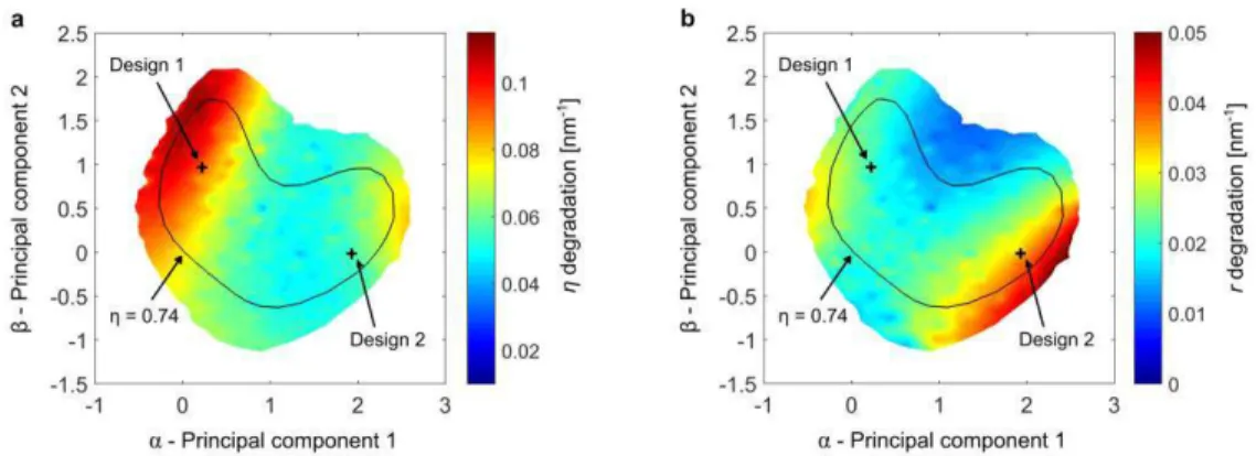
It is of particular interest also to investigate how the behaviour of the good gratings changes due to the unavoidable uncertainty generated by the fabrication. In particular, we assume a width deviation δ for both shallow and deeply etched sections caused by variabilities in the etch process. A good measure of the sensitivity of coupling efficiency and back-reflections to this variability is provided by a quantity denoted here as degradation derivative. This quantity is obtained by averaging the two directional derivatives with respect to positive and negative values of δ (see Methods). Given the results of the PCA, calculating this quantity for coupling efficiency and back-reflections can be done efficiently by scanning the limited region of good designs on the α-β hyperplane.
The computed values of the two degradation derivatives are shown in Figs. 4a and 4b. The black solid line contour marks the area with η > 0.74. The location of design 1 and design 2 described in Fig. 3 are shown as well. A high value of the degradation suggests a high sensitivity to width deviations. For the coupling efficiency, a particularly sensitive region is found close to design 1. On the contrary, the back-reflection is more sensitive to width deviations in the region close to designs 2. This region has a large overlap with the region of minimum back-reflection shown in Fig. 3d, making design 2 and surrounding designs high-performing when back-reflection is considered, but with stringent fabrication requirements. Design 3 is not marked in this figure since it is slightly above the α-β plane. In Supplementary we provide a direct verification of these results through a polynomial-chaos-based stochastic analysis15.
Fig. 4 Tolerance to fabrication uncertainty. The α-β hyperplane is exploited to investigate the sensitivity of possible good designs to fabrication uncertainty, assumed to be a width deviation for bothshallow and deeply etched sections in the grating. The maps show the value of the degradation derivative for (a) coupling efficiency and (b) back-reflections across the sub-space of good designs (η > 0.74, black solid line contour). Coupling efficiency of design 1 is very sensitive to width deviations compared to design 2. The opposite occurs for back-reflections, where design 2 has a much higher sensitivity than design 1.
10
Conclusion
The exploration and optimization of a high-dimensional design space in integrated photonics brings new challenges. The existence of large and possibly continuous set of degenerate designs with regard to a single performance parameter is the norm rather than the exception, but the comprehension of such a large design space is extremely difficult. In a change of perspective, in this Article machine learning pattern recognition methods are leveraged to describe and efficiently visualize the entire sub-space of degenerate good designs. Through designing a vertical grating coupler with state-of-the-art fiber coupling efficiency and obtain an initial small set of good design, we have demonstrated how the use of dimensionality reduction allows to identify two characterizing design parameters instead of the original five, significantly scaling down the complexity of the problem. Compared to global optimization techniques, this approach enabled an exhaustive mapping of the sub-space of good designs and the discovery of many designs with comparable fiber coupling efficiency but with significant differences in other performance criteria, such as back-reflections and tolerance to fabrication uncertainty.
We believe that the presented approach to design space exploration and comprehension, primarily based on the dimensionality reduction methods, is applicable to a wide range of problems. The use of principal component analysis is by no means limiting as the literature on machine learning dimensionality reduction extends well beyond linear methods, e.g. Kernel PCA36, Principal manifolds37 and Autoencoders38 just to mention a few. Furthermore, the results of dimensionality reduction techniques, that are statistical in nature, can lead to physical insights and reveal novel behavioral patterns of a particular device type that may be inconspicuous from the first principles.
Methods
Grating coupler simulation. The simulation of coupling efficiency and back-reflections for each design of the grating coupler is performed exploiting either a 2-D vectorial Fourier eigenmode expansion simulator35 or a commercial 2D-FDTD solver. We consider a structure including silicon substrate, 2- m buried oxide, 220-nm-thick silicon core and a silica overcladding of 1.5 m. Silicon and silica indices are assumed to be 3.45 and 1.45 at =1550 nm. The mode of a standard single-mode optical fiber SMF-28 vertically coupled on top of the grating is modeled with a Gaussian function with a mode-field-diameter of 10.4 m ( = 1550 nm). The fiber facet is assumed to be in direct contact with the top of the overcladding and its longitudinal position along the grating is optimized for each design to maximize the coupling efficiency. Coupling efficiency is calculated as the overlap integral between the simulated field diffracted upwards by the grating and the Gaussian function.
Machine learning enhanced optimization. We implemented a random-restart local search as the global
search technique for the optimization problem (1), although other global search algorithms could also be used. For each initial random design small perturbations are made until a better solution in terms of coupling efficiency is found and a line search is exploited to seek further improvement until convergence. The process then repeats until no improvement is found in the perturbation stage.
Following an initial optimization round with random-restart where a small collection of good designs was obtained, we trained a supervised machine learning model, specifically gradient boosted trees, to predict
11
if the radiation angle of a structure is within 5° of vertical. Once trained, we used the predictor to sample random designs that are nearly vertical while rejecting other random designs. Only near vertical emitting designs proceed to the local search stage as described above. The use of the predictor in the optimization led to approximately 250% increase in optimizer speed to find new designs meeting the coupling efficiency criteria η > 0.74
The performance of the general purpose machine learning predictor is comparable to that of a predictor based on the scalar grating equation relating the section lengths, effective indices and the radiation angle:
∑ ���� = + � sin 5 �= ⋅ ∑ �� 5 �= ,
where �, are constants related to the wavelength and the overcladding effective index, �� is the effective index of the i-th section, �� is the length of the i-th section, and is the radiation angle. Given the simulated data ( , �� , one can use linear regression to estimate all the constants and then use those to predict the radiation angle of the structure for any combination of the section lengths. Despite the fact that the general machine learning predictor is not aware of this approximation, its predictions are comparable to those using the above model. Furthermore, this approach can be applied to predict other quantities that cannot be described by simple closed-form expressions.
Hyperplanes definitions. As can be seen in equation (2), all the described hyperplanes are defined by three 5-D vectors V1, V2 and C, the latter being the reference origin within the hyperplane. For the two orthogonal hyperplanes Γ-Π and X-Π the vectors are found following linear algebra calculations by enforcing that the hyperplanes pass through certain points in space while being orthogonal to each other and orthogonal to the α-β hyperplane. The vectors are V1ΓΠ = [9.45, -0.35, -6.13, 45.95, -38.35] nm, V2ΓΠ = [-22.48, 33.08, 9.87, -17.87, -28.78] nm, C ΓΠ = [85, 84, 110, 289, 138] nm, V1XΠ = [25.92, 11.96, -44.16, 10.05, 12.61] nm, V2XΠ = V2ΓΠ, and C XΠ = [85, 84, 110, 284, 142].
Uncertainty model. For the investigation of design tolerance to fabrication uncertainty we assume a width deviation δ for both shallow and deeply etched sections, thus
L1’ = L1 – δ; L2’ = L2 + δ; L3’ = L3 – δ; L4’ = L4; L5’ = L5 + δ. We define a degradation derivative that is computed by averaging two directional derivatives, assuming that over and under-etch are equally likely (positive and negative values of δ can in general affect the device performance differently). Calculating the common derivative would not be informative as for locally optimized devices it would be close to zero. For coupling efficiency, we are interested in calculating
� (�+) �+ +
� �− −�− .
12
Acknowledgements
The authors gratefully thank to Dr. Mohsen Kamandar Dezfouli (National Research Council Canada) for providing detailed comments and suggestions on the manuscript.
Author contributions
D.M., Y.G., and D.X.X. conceived the strategy and developed the theoretical framework. Y.G. developed the machine learning algorithms. D.M. analysed the data and performed the stochastic analyses. P.C., A.S.P. and J.H.S. assisted in selecting the grating coupler study case. A.S.P. contributed to the development of the interface between the photonic simulator and machine learning algorithms. S.J., P.C., and J.H.S. provided theoretical and design guidance. D.X.X. and Y.G. supervised the project. All authors contributed to the discussion and manuscript writing.
References
1. Thomson, D. et al. Roadmap on silicon photonics. J. Opt. 18, 073003 (2016).
2. Smit, M. et al. An introduction to InP-based generic integration technology. Semicond. Sci. Technol. 29, 083001 (2014).
3. Cheben, P., Halir, R., Schmid, J. H., Atwater, H. A. & Smith, D. R. Subwavelength integrated photonics. Nature 560, 565–572 (2018).
4. Cheben, P. et al. Refractive index engineering with subwavelength gratings for efficient microphotonic couplers and planar waveguide multiplexers. Opt. Lett. 35, 2526–2528 (2010).
5. Frellsen, L. F., Ding, Y., Sigmund, O. & Frandsen, L. H. Topology optimized mode multiplexing in silicon-on-insulator photonic wire waveguides. Opt. Express 24, 16866 (2016).
6. Covey, J. & Chen, R. T. Efficient perfectly vertical fiber-to-chip grating coupler for silicon horizontal multiple slot waveguides. Opt. Express 21, 10886 (2013).
7. Håkansson, A. & Sánchez-Dehesa, J. Inverse designed photonic crystal de-multiplex waveguide coupler. Opt.
Express 13, 5440–5449 (2005).
8. Melati, D., Waqas, A., Xu, D.-X. & Melloni, A. Genetic algorithm and polynomial chaos modelling for
performance optimization of photonic circuits under manufacturing variability. in Optical Fiber Communication
13
9. Ma, Y. et al. Ultralow loss single layer submicron silicon waveguide crossing for SOI optical interconnect. Opt.
Express 21, 29374–29382 (2013).
10. Watanabe, T., Ayata, M., Koch, U., Fedoryshyn, Y. & Leuthold, J. Perpendicular Grating Coupler Based on a Blazed Antiback-Reflection Structure. J. Light. Technol. 35, 4663–4669 (2017).
11. Jensen, J. S. & Sigmund, O. Systematic design of photonic crystal structures using topology optimization: Low-loss waveguide bends. Appl. Phys. Lett. 84, 2022–2024 (2004).
12. Lalau-Keraly, C. M., Bhargava, S., Miller, O. D. & Yablonovitch, E. Adjoint shape optimization applied to electromagnetic design. Opt. Express 21, 21693 (2013).
13. Niederberger, A. C. R., Fattal, D. A., Gauger, N. R., Fan, S. & Beausoleil, R. G. Sensitivity analysis and optimization of sub-wavelength optical gratings using adjoints. Opt. Express 22, 12971–12981 (2014). 14. Su, L. et al. Fully-automated optimization of grating couplers. Opt. Express 26, 4023–4034 (2018). 15. Weng, T.-W., Melati, D., Melloni, A. & Daniel, L. Stochastic simulation and robust design optimization of
integrated photonic filters. Nanophotonics 6, 299–308 (2017).
16. Jensen, J. S. & Sigmund, O. Topology optimization for nano-photonics. Laser Photonics Rev. 5, 308–321 (2011). 17. Lu, J. & Vučković, J. Nanophotonic computational design. Opt. Express 21, 13351 (2013).
18. Piggott, A. Y. et al. Inverse design and demonstration of a compact and broadband on-chip wavelength demultiplexer. Nat. Photonics 9, 374–377 (2015).
19. Shen, B., Wang, P., Polson, R. & Menon, R. Integrated metamaterials for efficient and compact free-space-to-waveguide coupling. Opt. Express 22, 27175–27182 (2014).
20. Shen, B., Wang, P., Polson, R. & Menon, R. An integrated-nanophotonics polarization beamsplitter with 2.4 × 2.4 m2 footprint. Nat. Photonics 9, 378–382 (2015).
21. Liu, D., Gabrielli, L. H., Lipson, M. & Johnson, S. G. Transformation inverse design. Opt. Express 21, 14223 (2013).
22. Turduev, M. et al. Ultracompact Photonic Structure Design for Strong Light Confinement and Coupling Into Nanowaveguide. J. Light. Technol. 36, 2812–2819 (2018).
23. Peurifoy, J. et al. Nanophotonic particle simulation and inverse design using artificial neural networks. Sci. Adv. 4, eaar4206 (2018).
14
25. Michaels, A. & Yablonovitch, E. Inverse design of near unity efficiency perfectly vertical grating couplers. Opt.
Express 26, 4766 (2018).
26. Wang, B., Jiang, J. & Nordin, G. P. Embedded slanted grating for vertical coupling between fibers and silicon-on-insulator planar waveguides. IEEE Photonics Technol. Lett. 17, 1884–1886 (2005).
27. Roelkens, G., Thourhout, D. V. & Baets, R. High efficiency grating coupler between silicon-on-insulator waveguides and perfectly vertical optical fibers. Opt. Lett. 32, 1495–1497 (2007).
28. Dabos, G. et al. Perfectly vertical and fully etched SOI grating couplers for TM polarization. Opt. Commun. 350, 124–127 (2015).
29. Chen, X., Li, C. & Tsang, H. K. Fabrication-Tolerant Waveguide Chirped Grating Coupler for Coupling to a Perfectly Vertical Optical Fiber. IEEE Photonics Technol. Lett. 20, 1914–1916 (2008).
30. Pearson, K. On lines and planes of closest fit to systems of points in space. Lond. Edinb. Dublin Philos. Mag. J.
Sci. 2, 559–572 (1901).
31. M. Shenai, P., Xu, Z. & Zhao, Y. Applications of Principal Component Analysis (PCA) in Materials Science. in
Principal Component Analysis - Engineering Applications (ed. Sanguansat, P.) (InTech, 2012).
32. Kassahun, Y. & Kebedee, T. Application of Principal Component Analysis in Surface Water Quality Monitoring. in Principal Component Analysis - Engineering Applications (ed. Sanguansat, P.) (InTech, 2012).
33. Pasini, G. Principal Component Analysis for Stock Portfolio Management. Int. J. Pure Apllied Math. 115, (2017).
34. Dunteman, G. H. Principal Components Analysis. (SAGE, 1989).
35. Zavargo-Peche, L., Ortega-Monux, A., Wanguemert-Perez, J. G. & Molina-Fernandez, I. Fourier based combined techniques to design novel sub-wavelength optical integrated devices. Prog. Electromagn. Res. 123, 447–465 (2012).
36. Schölkopf, B., Smola, A. & Müller, K.-R. Nonlinear Component Analysis as a Kernel Eigenvalue Problem.
Neural Comput. 10, 1299–1319 (1998).
37. Gorban, A. N. Principal Manifolds for Data Visualization and Dimension Reduction. 58, (Springer Berlin Heidelberg, 2008).