Publisher’s version / Version de l'éditeur:
Journal of the Magnetics Society of Japan, 21, S2, pp. 491-494, 1997
READ THESE TERMS AND CONDITIONS CAREFULLY BEFORE USING THIS WEBSITE. https://nrc-publications.canada.ca/eng/copyright
Vous avez des questions? Nous pouvons vous aider. Pour communiquer directement avec un auteur, consultez la
première page de la revue dans laquelle son article a été publié afin de trouver ses coordonnées. Si vous n’arrivez pas à les repérer, communiquez avec nous à [email protected].
Questions? Contact the NRC Publications Archive team at
[email protected]. If you wish to email the authors directly, please see the first page of the publication for their contact information.
NRC Publications Archive
Archives des publications du CNRC
This publication could be one of several versions: author’s original, accepted manuscript or the publisher’s version. / La version de cette publication peut être l’une des suivantes : la version prépublication de l’auteur, la version acceptée du manuscrit ou la version de l’éditeur.
For the publisher’s version, please access the DOI link below./ Pour consulter la version de l’éditeur, utilisez le lien DOI ci-dessous.
https://doi.org/10.3379/jmsjmag.21.S2_491
Access and use of this website and the material on it are subject to the Terms and Conditions set forth at
High sensitivity and broad bandwidth magneto-impedance effect in
magnetic microstrip lines
Jiang, Nianhua; Yamakawa, Kiyoshi; Honda, Naoki; Ouchi, Kazuhiro
https://publications-cnrc.canada.ca/fra/droits
L’accès à ce site Web et l’utilisation de son contenu sont assujettis aux conditions présentées dans le site LISEZ CES CONDITIONS ATTENTIVEMENT AVANT D’UTILISER CE SITE WEB.
NRC Publications Record / Notice d'Archives des publications de CNRC:
https://nrc-publications.canada.ca/eng/view/object/?id=78ed32db-bd16-471d-b9fb-34badd594d79 https://publications-cnrc.canada.ca/fra/voir/objet/?id=78ed32db-bd16-471d-b9fb-34badd594d79© 1997 by The Magnetics Society of Japan
High Sensitivity and Broad Bandwidth Magneto-Impedance
Effect in Magnetic Microstrip Lines
Nianhua Jiang, Kiyoshi Yamakawa, Naoki Honda and Kazuhiro Ouchi Akita Research Institute of Advanced Technology
4-21 Sanuki, Araya, Akita 010-16, Japan
Abstract - A unique magneto-impedance effect by directly flowing microwave power in a Magnetic Microstrip Line was investigated. The microwave can be modulated by external fields that caused the impedance change due to the permeability variation in the magnetic strip. The amplitude variation of the microwave carrier was rectified to obtain output signals. A simple structure sensor has been developed that exhibited a high sensitivity of 10 mY/Oe, a high changing ratio of 48% in the transmission-line impedance and a broad signal bandwidth of 300 MHz. This sensor has great advantages of high sensitivity and broad bandwidth over MI sensors previously proposed. Key words: Magnetic sensor, Magneto-Impedance, Magnetic microstrip line, Transmission-line impedance, Broad bandwidth, High sensitivity.
I. INTRODUCTION
Steady and substantial advancements in magnetic recording technology have been continually undertaken. Typically, by using MR and GMR heads considerable progresses have been achieved in areal densities. Since the data transfer rate becomes very important for the high areal density over 20 Gbit/in2, a head needs to maintain a high performance at very high frequencies (over 200 MHz). Therefore, a high sensitivity together with a broad signal bandwidth must be required for the head to meet high areal density as well as high data rate recording. Utilizing conventional heads such as inductive heads and etc. that were composed of lumped constant circuits, it seems difficult to achieve such a broad bandwidth. Some new principles should be explored for heads to operate efficiently at very high frequencies.
A magneto-impedance sensor was discussed with amorphous magnetic wires having 30 11 m in diameter and 5 mm in length [1]. Moreover, an LC resonance circuit with a soft magnetic film strip was proposed to detect magnetic fields in [2]. An RF power was supplied to
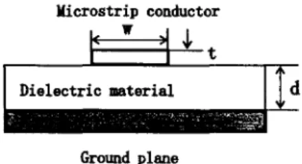
Kicrostrip conductor 11'
d Ground plane
Fig. 1 Cross sectional view of a microstrip
excite the resonance circuit. Thus, an external field can modulate the RF voltage in the circuit by inducing variations of the resonance frequency and the Q of the LC circuit due to the permeability change in the magnetic strip. Because its performance was based on resonance, the sensitivity was inversely proportional to its bandwidth. It
implied that both high sensitivity and broad bandwidth could not be satisfied simultaneously.
A one-turn thin film head [3] was also presented on the same principle as that of the reference [2]. By using an impedance matching circuit, efforts were made to increase the sensitivity and achieved experimentally the -3 dB bandwidth of 70 MHz [4]. A sensor utilizing resonance circuits [2] seems difficult to show much broader bandwidth. When RF carrier frequencies become higher and higher, the transmission loss induced in those circuits may turn so large that the sensor can not work effectively.
In [5] YIG films was inserted into dielectric slabs under a microstrip conductor to construct a filter working on magnetostatic wave mode, so that RF current did not directly flow through the YIG films.
In this study, a unique magneto-impedance effect is described by introducing a magnetic microstrip line, which leads to develop a new sensor of high sensitivity and broad bandwidth. This sensor is much simpler in the structure than those proposed previously.
11. PRINCIPLE
A cross sectional view of the microstrip line used for a microwave transmission line is shown in Fig. 1. It
consists of a microstrip conductor, a ground plane and a dielectric substrate. According to the theory of guided waves [6], the characteristic impedance of microstrip lines is just related to the dielectric constant and dimensional parameters such as width and thickness of the microstrip conductor, and thickness of the dielectric. This structure
Hex Output ( ZI) IZ セ@
セ@
$'
'"
InputNセ@
AェN[B[セMMMKセセᄃ]セセセ@
o ' Magnetic strip Substrate Ground planeFig. 2 Schematic of the new magnetic sensor utilizing a Magnetic Microstrip Line.
A
z.
BセdMMMMMMMM[」ZZjイMMMMMMMMセo@
z.
z.
o o
Fig. 3 Equivalent circuit of the sensor
can transmit microwaves or even milli-waves. It means that the structure has a very broad bandwidth up to tens of gigahertz. We replaced the microstrip conductor with a magnetic thin film strip to construct a magnetic microstrip line as shown in Fig. 2. Needless to say, the ground plane is very essential for this structure. A microwave power enters into the port A and propagates through the magnetic microstrip line, then comes out at the port B. A principal equivalent circuit of the new sensor is illustrated in Fig. 3 where
z.,
is a characteristic impedance at the port A and B, Zm is a transmission-line impedance of the magnetic strip. When external magnetic fields are applied along the longitudinal or transverse direction of the magnetic strip, the permeability under the carrier frequency will change with the external field. Thus, the transmission-line impedance Zm also varies as a function of the external field.Practically, the microwave magnetic (RF) field is in the cross section of the magnetic strip. There is an interaction between magnetic moments and the RF field as shown in Fig. 4. When the magnetic thin film strip is prepared with its anisotropy field Hk along the transverse direction and the external magnetic field Hex is applied at the hard axis of the magnetic strip, the moment in the strip tends to rotate parallel to Hex' and precesses concurrently around it. Hex can adjust the moment angle, which results in variations of the transmission-line impedance. Therefore, the external magnetic field can modulate the propagation of the microwave in the magnetic microstrip line. We can pick up the signal by measuring the amplitude variation of the microwave at the port B. On the other hand, when the easy axis is arranged in the longitudinal direction of the magnetic strip as shown in Fig. 5, the magnetic moment will precesse around Hex under the RF field. The external magnetic field can also modify the permeability by changing the deflection of moments. The principle of this new MI sensor described here seems similar to those proposed in the past [1] [2], but the transmission effect is very different from the resonance.
Hex
)
Easy axis
Fig. 4 Illustration of precession of magnetic moments in the magnetic strip under RF fields and He. 11 im..LHk.
Hex Microwave セ@
ゥセBLNy@
---ff
(1
I
RF fields ( ) Easy axis Fig. 5 Illustration of precession of magnetic moments in the magnetic strip under RF fields and He. 11 Hk 11 im .By selecting dimensional parameters, dielectric constant
and etc., the characteristic impedance of the magnetic
microstrip line should be designed to match the system impedance to be connected with it. If we can do so, this sensor could work at gigahertz band and be expected to achieve hundreds of megahertz bandwidth without any impedance matching circuits. The new sensor structure is very simple and seems to avoids the problems of circuit resonance. Hence, it is expected to result in reduction of the transmission loss of the carrier and robustness against the noise from outside in contrast with a lumped constant circuit.
Ill. SENSOR FABRICATION
A magnetic thin film of amorphous C085.6Zr5.2Nb9.2
(wt%) (Bs
=
1.25 T) was first deposited by RF magnetronsputtering on a glass substrate of 1 mm thick. Its magneto-striction constant is less than 10-6• During the sputtering a static magnetic field of 30 Oe was applied parallel to the substrate to induce an uniaxial anisotropy in the film plane. Then under the pressure of 5 X 10.6 Torr, the film was
annealed at 300'C for 1 hour in an ac magnetic field to increase its permeability, followed by annealing in a dc magnetic field of 1 kOe to adjust the anisotropy field Hk =
8 Oe for getting a sharp distribution of magnetization in easy axis.
The magnetic strip was formed by photo-lithographic processes and ion beam etching. A Cu film of 2 11 m thick was deposited by dc sputtering for a pair of microstrip conductors at the in and out ports. A 3 11 m thick ground plane of Cu was finally deposited by de
150 loo-o -150
I
n-
rl
--75 o 75 150 Hex (Oe)Fig. 6 External field dependence of the output at the carrier of 1 GHz and 50 mW power under He. 11 im..LHk•
10 セMMセMMMMセMMMMセMMセ@ 8 セVエMMMGイゥjMMMKMMMMMエNiヲMMMMMi@ セ@ 4 1----fJ'II, 0 ... ---'----... - - -... ---1 -400 -200 0 200 400 Hex (Oe)
Fig.7 External field dependence of the output at the carrier of 1 GHz and 50 mW under H •• "Hk..Lim•
sputtering on the back of the substrate. To improve the adhesive strength of Cu, a very thin film of Ti was deposited as an underlayer before the deposition of Cu.
External magnetic fields were applied with Helmholtz coils. By means of a network analyzer (0 - 1.8 GHz) connected with a S-parameter test set, the output voltage was obtained from rectifying the amplitude variation of the microwave at port B with coaxial cables of 50 Q.
IV. RESULTS AND DISCUSSION
First, a sensor with the magnetic strip (1 JL m X 250 JL
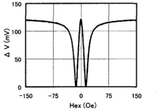
m X 2.5 mm) was evaluated at a carrier frequency of 1 GHz. We measured the case of the easy axis in transverse direction of the magnetic strip and Hex applied longitudinally. The external field dependence of the output, named as a W -type curve, was shown in Fig. 6.
The output voltage rapidly changed with the external field. When Hex increased to the value of the anisotropy field Hk ,
magnetic moments almost turned to the direction of Hex. In this case the RF permeability was at the maximum, so the impedance got to the largest, and then the carrier output became the minimum. Further increasing Hex caused the deflective angle of moments to reduce and the permeability to decrease. When Hex was over 100 Oe, moments could not respond to the RF field. The output of 120 m V was obtained at the input power of 50 mW. The high sensitivity of 9.2 mV/Oe has been achieved under the field of 13 Oe. When Hex was applied in the transverse
100 セ@ 75 > 50 <I 25 i::=-o -150
'\
r
-75 0 75 150 Hex (Oe)Fig. 8 External field dependence of output at the carrier of 1 GHz and 50 mW under H •• "Hk "im .
100 75
セ@
> 50 <I 25 o--
セ@,
-320 -160 , /(
\
J
o 160 320 Hex (Oe)Fig. 9 External field dependence of the output at the carrier of 1 GHz and 50 mW under H •• ..LHk "im•
direction, the different profile was obtained as shown in Fig. 7. In this case Barkhausen noise was severe due to domain wall motion and Barkhausen jump.
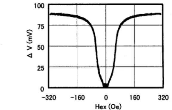
Furthermore, a sensor with the magnetic strip (1 JL m X
250 JL m X 2.5 mm) was evaluated whose easy axis was in
longitudinal direction. Figure 8 exhibits the dependence of the output on the external magnetic field applied longitudinally. At Hex
=
0, magnetic moments were in free state and the permeability and impedance were at the largest, so that the output came to the minimum. As Hex was increased, like previous description, the permeability and impedance reduced, then the output increased. The maximum sensitivity of 9 mV/Oe was obtained near Hex=
O. While Hex was applied in transverse direction, the profile was obtained as shown in Fig. 9. Since there was the demagnetized field in the transverse of the strip, the high sensitivity area was shifted to about the field of 60 Oe.
Finally, a micro-sized sensor (1 X 5 X 50 JL m) was investigated whose easy axis was made in transverse direction. The external magnetic field dependence of the output was shown in Fig. 10 under Hex applied longitudinally. Since there was a strong shape anisotropy in the length direction in this case, the magnetic moment ranged in the length direction. Therefore, figure 8 and 10 exhibited the same V-type curve. The output of 19 mV was obtained at the input power of 1 m W. A high changing ratio of 48% of the transmission-line impedance
25
-
セ@
r:-
-\
\I
20セ@
15 > <I 10 -150 -75 0 75 150 Hex (Oe)Fig. 10 External field dependence of the output at the carrier of 1 GHz and 1 mW.
1000 :; 100 -5 )(
..
E > <3 10 セ@L
0.01 0.1 10 100 Carrier power (mW)Fig. 11 Carrier power dependence of the output at the carrier frequency of 1 GHz.
has been achieved with Zm changing from 7.7 to 11.5 Q. Moreover, the carrier power dependence of the maxim-um output voltage (l:l V m.x) of the same sensor in Fig. 10 is shown in Fig. 11 at the carrier frequency of 1 GHz. The output voltage was defined as the amplitude difference between the external fields of 50 and 0 Oe. Obviously, the output voltage was almost proportional to the square-root of the carrier power in the range from 0.01 to 100 mW. The
z.,
was not yet designed to match the system impedance. Although thez.,
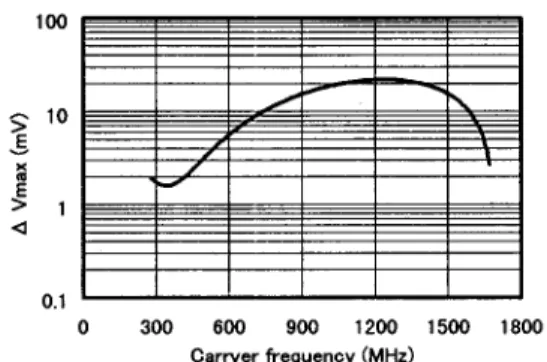
is 32 Q at 1 GHz, the large output of 122 mV was achieved at the input power of 100 mW. The high sensitivity of 10 mV/Oe was accomplished under the field of 2 Oe. No saturation was observed in the output up to 100 mW that was the maximum analyzer power in the measurement. These results indicate that a higher reproducing output would be obtained by increasing the carrier power.Its carrier frequency response of the maximum output voltage is shown in Fig. 12 where the input power was 1 mW. The ferromagnetic resonance frequency is predicted about 2.4 GHz. The -3 dB bandwidth of 600 MHz was realized around the carrier frequency of 1 GHz in this case. The useful signal bandwidth of 300 MHz was attained without any impedance matching circuits. These performances of the sensor were essentially distinct from those of conventional sensors. The design of Zo was not yet performed in this paper. It is also expected to further improve the performance by matching the impedance.
V. CONCLUSION
The magnetic microstrip line was introduced to construct a new magnetic flux sensitive sensor operating by use of a microwave carrier. The unique magneto-impedance effect was investigated and found to have different profiles by orientations of the anisotropy and external magnetic field. One of the novel sensors has demonstrated the high sensitivity of 10 mV/Oe, the high changing ratio of 48% in the transmission-line impedance and the broad signal bandwidth of 300 MHz without special matching circuits. This sensor is of micro-sized, very simple and easy to be prepared by thin film processes.
100 :; 10 -5 )(
..
E > 1 <3 0.1 o . /....
t-. p 300 600 900 1200 1500 1800 Carryer frequency (MHz)Fig.12 Carrier frequency dependence of the output at the input power of 1 mW.
It will not only be used as a field sensor but also be suitable for a reproducing head for future magnetic recording of high areal density as well as high data rate. Moreover, it is also very interesting to explore its applications in other areas.
VI. ACKNOWLEGMENT
The authors wish to express gratitude to President S. Iwasaki, of Tohoku Institute of Technology, for his advice and encouragement. We also thank Mr. S. Takahashi, Mr. K. lse, and Ms. K. Taguchi for their help in the experiments.
REFERENCES
[1] K. Mohri, et al. "Magneto-Impedance Element", IEEE Trans. Magn., Vo!. 31, No. 4, P2455-2460, July 1995.
[2] J. Akiyama, et af. "Magnetic Read-Out Head Using Induced RF Permeability Variation", IEEE Trans. Magn., Vo!. 22, No. 5, P692-694, September 1986.
[3] M. Senda, et al. "Extremely High Output of UHF Carrier Type Head with Impedance Matching Network", IEEE Trans. Magn., Vo!. 32, No. 5, P3485-3487, September 1996. [4] M. Senda, et al. "High Frequency Signal Response of
Impedance Matched UHF Carrier Type Head", Digests of INTERMAG'97, New Orleans, Louisiana, GP-18, April 1-4, 1997.
[5] M. Tsutsumi, et al. "Band Rejection Filter of Microstrip Lines Using Yttrium-Iron-Garnet Film", Technical Report of IEICE, MW90-57.
[6] R. E. Collin, Field Theory of Guided Waves. McGraw-HiII Book Company Inc., New York, 1960.
[7] Y. Sugiyama, et al. "The FMR Magnetic Reproducing Head Using A Microwave Guide", IEEE Trans. Magn., Vo!. 29, No. 6, P3867-3869, November 1993.
[8] M. Takezawa, et al. "Micro Magnetic Thin-Film Sensor Using LC Resonance", Digests of INTERMAG'97, New Orleans, Louisiana, HC07, April 1-4, 1997.