HAL Id: hal-02326959
https://hal.archives-ouvertes.fr/hal-02326959
Submitted on 31 Oct 2019HAL is a multi-disciplinary open access archive for the deposit and dissemination of sci-entific research documents, whether they are pub-lished or not. The documents may come from teaching and research institutions in France or abroad, or from public or private research centers.
L’archive ouverte pluridisciplinaire HAL, est destinée au dépôt et à la diffusion de documents scientifiques de niveau recherche, publiés ou non, émanant des établissements d’enseignement et de recherche français ou étrangers, des laboratoires publics ou privés.
Structural and textural changes of CVD-SiC to
indentation, high temperature creep and irradiation
Georges Chollon, Jean-Marie Vallerot, Doriane Helary, Stéphane Jouannigot
To cite this version:
Georges Chollon, Jean-Marie Vallerot, Doriane Helary, Stéphane Jouannigot. Structural and textural changes of CVD-SiC to indentation, high temperature creep and irradiation. Journal of the European Ceramic Society, Elsevier, 2007, 27 (2-3), pp.1503-1511. �10.1016/j.jeurceramsoc.2006.05.038�. �hal-02326959�
Available at: https://doi.org/10.1016/j.jeurceramsoc.2006.05.038
STRUCTURAL AND TEXTURAL CHANGES OF CVD-SiC TO INDENTATION, HIGH TEMPERATURE CREEP AND IRRADIATION
G. CHOLLON1*, J.M. VALLEROT1, D. HELARY1,2 and S. JOUANNIGOT1
1 Laboratoire des Composites Thermostructuraux (LCTS), UMR 5801 (CNRS-SNECMA-CEA-UB1), Université Bordeaux 1, 3, allée de La Boétie, 33600, Pessac, France
2 Commissariat à l’Energie Atomique, CEA/DEN/VRH/DTEC/STCF, BP 111, 26702, Pierrelatte, France
ABSTRACT
The structure and microtexture of different SiC based CVD coatings have been studied by RMS, in their as-processed state and after high temperature annealing, creep, indentation and irradiation. Both annealing and creep resulted in the same degree of SiC crystal growth and decrease of stacking faults. A slight influence of stress was however observed on the structure and texture of the co-deposited free-carbon, likely as a consequence of the intergranular creep mechanism. Room temperature indentation induces substantial structural disorders (dislocations, stacking faults, small grains) near the contact and more extended damages due to dislocation slip parallel to the compact Si-C planes. These structural changes were found to depend on the single crystal orientation and therefore, on the texture of
* Corresponding author: Tel.: +33 5 56 84 47 27, Fax: +33 5 56 84 12 25, E-mail address:
polycrystalline SiC. Room temperature proton irradiation produced only small amounts of disorders. The specific alterations of the Raman features were explained using a phonon confinement model. This approach supports the existence of very low scale defects, likely as punctual defects.
Key Words: Defects (B.); Creep (C.), Plasticity (C.); SiC (D.); Raman Spectroscopy
1 INTRODUCTION
Chemical vapour deposited silicon carbide (CVD-SiC) is an excellent candidate for high temperature structural applications, because of its exceptional range of mechanical and thermal properties. CVD-SiC is deposited for instance on tungsten or carbon monofilament cores, for the reinforcement of metal matrix composites.1-3 The filaments obtained display outstanding mechanical properties such as high strength, stiffness and creep resistance. CVD-SiC coatings are also constituents of the nuclear fuel particles which are considered for the fourth generation fission reactors.4 The CVD-SiC layer is inserted between two dense pyrocarbon layers to retain the fission products and maintain the mechanical and thermal properties of the particles under neutron irradiation at high temperature.4 Depending on the CVD conditions, the stoichiometry (i.e., the occurrence of free silicon or carbon phases), the crystal structure and the texture (the main orientation of the SiC crystals) in the coatings may vary, with a significant effect on the thermal and mechanical properties at room, high temperature,2 and under irradiation.
Raman Microspectroscopy (RMS) is a non-destructive technique which provides information, at the micrometer scale, on the phase composition and the crystalline state (structure and texture) of materials. It is therefore particularly suited to the local analysis of
few micrometers-thick CVD coatings.3 The aim of the present paper is to investigate the structural and textural evolution of various CVD-SiC coatings, induced by room and high temperature plastic deformations and by irradiation. For this purpose, the specimens, a commercial SiC-CVD filament and a model C/SiC/C/ZrO2 nuclear fuel particle, were submitted to (i) tensile creep at high temperature, (ii) indentation at room temperature and (iii) proton irradiation at room temperature.
2 MATERIALS AND EXPERIMENTAL PROCEDURE
6H-SiC crystals were used as a reference material for the structure and texture analyses through RMS analyses, as well as for the indentation and irradiation tests. The CVD-SiC monofilament (SCS-6) is a carbon core 140m filament produced by Textron Specialty Materials. The CVD-SiC sheath is carbon rich near the carbon core and near stoichiometric (with a slight excess of free silicon) near the surface.1-3 It is subsequently covered by a 3m multilayer pyrocarbon (PyC) coating. The HTR (High Temperature Reactor) model nuclear fuel particle consists of a 500m ZrO2 core successively coated with a buffer porous pyrocarbon layer (95m), a dense PyC inner layer (40m), the 35m-thick CVD-SiC layer and a dense PyC outer coating (40m).
The longitudinal tensile creep testing of the monofilaments was achieved in high vacuum with a resistive heating device (isothermal gauge L0=50mm). The load and temperature were applied during 2.2 104s at 300MPa and 1400°C, respectively. To dissociate the effects of the annealing and/or the applied stress, a second non-loaded filament was simultaneously tested.
The indentation tests (MTS XP) were carried out with a diamond Berkovich tip at a maximum load of 300mN.
The proton irradiation experiments were carried out at the Phase Laboratory (Strasbourg, France). The energy, the current and the fluence were 4MeV, 0.6Acm-2 and 3.1016cm-2, respectively.
The Raman analyses were performed with a Labram HR (Jobin Yvon) microspectrometer (=632.8nm, spectral resolution 2cm-1, lateral resolution 1m). A motorized micro-displacement stage (0.1m) was used for the linescan and mapping measurements. The incident laser light propagating along the X axis of the laboratory, was plane polarised along the vertical Y axis (Tables 1-2). The back-scattered light (configuration X<Y.>-X) was analysed either without (X<Y(Y+Z)>-X) or using a rotating polariser. Two scattering arrangements were used in the later case, (i) X<YY>-X or <YY>, (polarisation of scattered light along Y) and (ii) X<YZ>-X or <YZ> (polarisation along the horizontal Z axis). The configuration <ZZ> was also examined by simply rotating the specimen of an angle /2 and analysing the <YY> polarization.
3 RESULTS AND DISCUSSION
3-1 Raman features of SiC-based materials
SiC exists in a variety of metastable polytypes. Only one is cubic (-SiC, zinc blende structure), the others are either hexagonal (2H (wurtzite), 4H, 6H) or rhombohedral (15R, 21R). The 3C-SiC unit cell has a Td symmetry yielding one triply degenerate Raman active phonon (T2x, T2y, T2z). This mode is polar and leads to an energy difference between the vibration polarised parallel to the wavevector of the phonon q (longitudinal optic: LO) and that polarised perpendicular to q (transverse optic: TO). In 3C-SiC, two Raman peaks are therefore observed corresponding to the TO and LO modes at 796cm-1 and 972cm-1, respectively. The point group for the hexagonal polytypes is C6v. It gives rise to the Raman
active A1, E1 and E2 modes. Both E1 and E2 are doubly degenerate (E1x,E1y and E21,E22) and only A1 and E1 are polar and split into TO and LO phonons.5 As the unit cell increases, additional phonons with different energies may appear. These new Raman bands are called folded modes, as they correspond to phonon modes located within or at the edge of the Brillouin zone.6 Their frequencies are obtained by folding the dispersion curves of the 3C polytype phonon modes (two optic: TO and LO and two acoustic LA and TA branches) to the centre of the Brillouin zone (q=0). Hence, acoustic phonons resulting from the folding of the acoustic branches are observed for the hexagonal polytypes, whereas they are forbidden for the 3C polytype.
Amorphous and/or cubic silicon, or sp2 carbon are sometimes co-deposited in particular CVD conditions. The space group for cubic silicon is Oh and gives rise to a triply degenerate Raman active phonon (T2g1, T2g2, T2g3) at 521cm-1. The Si amorphous state is characterized by broad band around 480cm-1. The space group corresponding to hexagonal graphite cell is D6h and only phonons with the E2g symmetry are Raman active. In addition to the main E2g mode (referred to as the G band at 1580cm-1), the spectra of sp2 carbons generally exhibit features assigned to structural disorder (e.g., the D and D’ bands around 1335 and 1615cm-1, respectively). Their intensity and width both increase with the amount of disorder.7
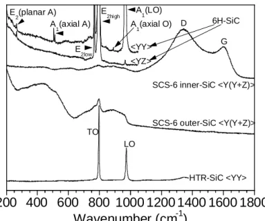
Except E1(LO) (which is not observable in the back-scattering geometry), all the optical phonons characteristic of the 6H-SiC phase (E2(low)=767cm-1, E2(high)=789cm-1, E1(TO)=798 cm-1 and A1(LO)=966cm-1) are clearly identified on the Raman spectra recorded for various polarisations and orientations of the SiC single crystal (Fig. 1). Besides these strong optical modes, a weak additional A1(LO) peak is observed at 889cm-1, together with several acoustic features (E1(TA)=240cm-1, E2=266cm-1, A1(LA) doublet at 505 and 514cm-1).
The cross section of the SCS-6 filament has been examined by RMS. The Raman analyses confirm the dual structure of the CVD-SiC sheath, consisting of a carbon rich SiC
layer near the carbon core (as shown by the presence of the D and G bands) and a near stoichiometric SiC outer layer (Fig. 1).1-3 The broad carbon features correspond to a very disordered form (turbostratic, with heavily distorted graphene layers). The various optical modes evidenced for the 6H-SiC crystal are also present for the outer CVD-SiC. The Raman peaks appear at similar frequencies but with larger widths and overlapping, due to a lower crystalline state. Very large bands below 600cm-1 (due to acoustic phonons) and at 600-1000cm-1 (characteristic of a density of state) are also observed. These broad bands are likely due to the scattering of sub-micron size crystals and/or grain boundaries. The occurrence of multiple overlapping modes in the TO region (750-810 cm-1) does not support the existence of pure cubic or hexagonal polytypes. These features are rather characteristic of a coherent structure involving a high density of stacking faults along the [111]-cubic or [001]-hexagonal direction (i.e., along the compact Si-C planes direction).
The Raman spectra from the cross section of the SiC-CVD sheath of the HTR particle show mainly two sharp peaks at 796 and 772cm-1, typical of the 3C polytype and a very weak component at 767cm-1, probably due to a low proportion of stacking faults (Fig. 1). No evidence of any secondary phase could be shown.
3-2 Influence of the crystal orientation on the phonon intensities
The intensities of the various phonons vary with the orientation of the crystal (xyz) about the laboratory axes (XYZ). The scattering efficiency (I) is related to the polarization of the incident (ei) and scattered (es) light and is given by I=C
j |ei.R(j).j.es|2, where C is a constant, Rj is the Raman tensor and j is the polarization of the phonon j.8 The expressions of the Raman tensors were given by Loudon for the various crystal symmetry classes.8 For both Td and Oh, the crystal coordinate system (x, y, z) is chosen along the [100], [010] and [001] crystal axes, whereas for C6v, the z axis is taken as the c [001] direction and the x and y axesare perpendicular to z and to one another. For the D6h symmetry, the tensors for the non polar Raman active E2g1 and E2g2 modes are respectively equivalent to the E2(1) and E2(2) above expressions. The T2, A1 and E1 modes are polar. The intensities of the LO and TO vibrations therefore vary with the propagation directions in the crystal (Table 1-2). In the back-scattering configuration, q is parallel to the light propagation, i.e., to the X axis of the laboratory. The consequence is straightforward for both the A1 and E1 modes, as A1(LO) is active when q is along the c axis of the crystal, whereas the A1(TO) and E1(TO) modes are active when q is perpendicular to c. For the cubic zinc-blend crystal, the assessment of the TO and LO peak intensities is more complex. It can be shown, for instance, that the TO mode is strictly forbidden for the [100] crystal orientation, whereas the LO mode is forbidden for the [110] orientation. The calculated phonon intensities as a function of the scattering geometry and the main crystal orientation is given in Table 1-2. The intensity factors of the TO-LO components have been marked out (e.g., e and e’) due to the different electro-optic coefficients.9
The selection rules of the various TO and LO-region phonons, for the cubic and the hexagonal SiC polytypes, show only few common features when considering the orientation of the compact Si-C plane axes with respect to the X axis. For instance, the influence of the polarization configuration and the rotation angle of the crystal about the X axis is similar when examining (i) respectively the T2(TO) and the T2(LO) modes, for the cubic-[111] crystal orientation and (ii) the E2 and the A1(LO) modes, for the hexagonal-[001] direction (Table 1-2). Conversely, if the dense Si-C plane axis is perpendicular to the X axis (i.e., when analysing the [112]-cubic and [100]-hexagonal crystal face respectively), the A1(LO) mode is forbidden for all polarizations, whereas the T2(LO) mode appears in certain polarization conditions.
Raman spectra were recorded from the 6H-SiC crystal with different orientations. All the optical modes and most of the acoustic features are well identified and obey strictly the above
selection rules (Table 1). The high intensity peak at 789cm-1 was shown to be a superposition of two phonons with A1(TO) and E2 symmetries.5 The measured intensities were used to determine the characteristics of the analyzer (efficiency, transmittance) and the parameters a, b, c and d of the Raman matrices. RMS measurements were also performed as a function of the rotation angle of the 6H-SiC crystal about the X axis (laser axis), with X either parallel or perpendicular to the c [001] axis.10 Intensity predictions were also made for both cubic and hexagonal systems. When the [111]-c or the [100]-h axes are parallel to the X axis, the intensities of the T2(TO) and T2(LO) modes, and the A1(LO) and E2 modes respectively, remain constant whatever . Conversely, when the [111]-cubic or [100]-hexagonal axes are perpendicular to X, the intensities of the T2(TO), T2(LO), A1(TO), E1(TO) and E2 modes vary significantly with and follow sinusoidal laws of periods or /2. The experimental data obtained from the 6H-SiC crystal were found to match the calculated intensities very accurately. This approach was used to analyze the texture of the various CVD-SiC coatings.
3-3 Structure and texture analysis of the as-processed materials
The cross sections of both the as-processed SCS-6 filament and the HTR fuel particle were submitted to RMS mappings. RMS mappings with the two scattering configurations (X<YY>-X and X<YZ>-X) were recorded to examine the effect of the coating orientation on the phonon intensities, to evidence any preferential orientation of the crystallites. The intensity of the various modes was computed for all spectra along the cross-section and plotted as phonon intensity, bandwidth (FWHM) or frequency linescans or mappings (figure 2-3).
The HTR particle is fully stoichiometric throughout the whole section whereas the dual inner carbon rich/outer stoichiometric structure of the CVD-SiC filament appears clearly on the Raman intensity mappings for the SiC and carbon features (Fig. 2-3). The cross sections
of the filament and the HTR particle are both circular. The punctual analysis of the SiC coating as a function of the rotation angle about the X axis is therefore equivalent to the tangential scanning analysis of the coating. The anisotropy of the SiC-CVD coatings of the SCS-6 filament is clearly noticeable from the symmetrical SiC features intensity patterns. The mappings show either two or four center-symmetrical minima/maxima spots, the geometry of which is characteristic of the phonon symmetry (Fig. 3). These features are explicitly related to the periodic intensity functions (of periods or /2) established above for the SiC crystal as a function of the rotation angle about X, when the [111]-c or [100]-h direction is perpendicular to X. The preferential orientation of the dense Si-C planes normal to the CVD growth direction is clearly established. The cubic or hexagonal selection rules are obviously not strictly obeyed, due to the faulted SiC structure and the angular dispersion of the crystals in the coating. However, such a coherent SiC structure containing random or periodic stacking faults along a single anisotropy direction, gives rise to phonon symmetries closer to those of the 6H-structure than 3C. This is confirmed for instance by the absence of the LO feature on the spectra from the transverse filament cross section whereas it is observed from a longitudinal cross section.
The TO and LO mappings of the HTR particle show contrasted domains of a few micrometers (i.e., larger that the spatial resolution) related to -SiC crystals with different orientations. The peripheral scan along the coating did not reveal any variation of the average intensity values, suggesting that the polycrystalline -SiC coating is isotropic. The absence of texturing was indeed confirmed by TEM analyses, although a slight preferential orientation was observed by electron back scattering diffraction.
Both the annealed (T=1400°C, t=2.2 104s, =0MPa) and crept (T=1400°C, t=2.2 104s,
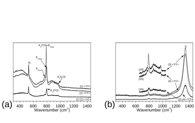
=300MPa) SCS-6 filaments were submitted to RMS analyses and compared to the as-processed specimens. The RMS analyses did not evidence any change in the radial distribution of the SiC and free carbon phases. However, the near stoichiometric outer region of both the annealed and crept specimens showed the presence of a sharp peak at 524cm-1, indicative of the presence of crystallized free silicon (Fig. 4). The cubic silicon phase segregates and crystallizes from the initial amorphous intergranular phase which is co-deposited by CVD (at about 1100°C). The relatively high frequency of the silicon peak (521cm-1 expected in cubic Si) denotes a significant compressive stress state, likely due the SiC/Si thermal expansion mismatch.
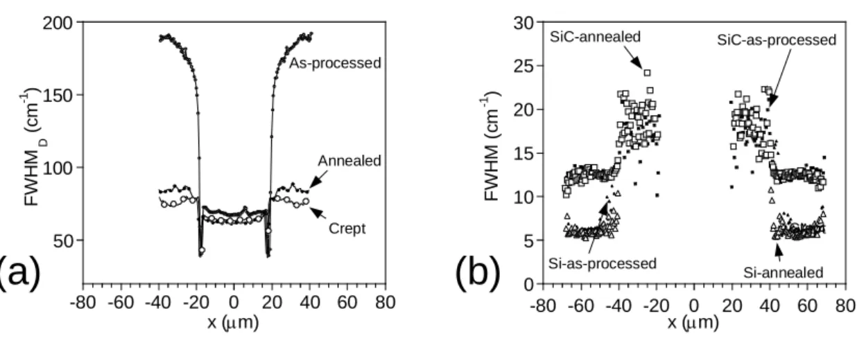
In order to assess the structural changes induced by the annealing/creep tests, the bandwidths of the various characteristic peaks were examined through the diameter of the filaments (Fig. 2). The bandwidth (FWHM) is indeed directly related to the crystal size for both silicon and SiC. The FWHM values of both the G and D bands also vary significantly with the structure of pyrocarbons. They are rather related, in this case, to the in-plane local defects or wrinkled graphene layers.
The presence of co-deposited free carbon in the inner region of the as-processed filament is associated to a smaller SiC grain size (or a larger bandwidth) than in the near stoichiometric outer region (Fig. 2). The same holds true for the annealed and crept specimens. However, a significant increase of the grain size is observed after both annealing and creep (20% decrease of FWHM), indicating a predominant influence of the temperature with respect to stress. A much more considerable decrease of the FWHM value of the D band is observed after annealing and creep (of about 50%) , which is associated to a significant ordering of the graphene layers (Fig. 2). A slight effect of the stress is also discernible. It is generally admitted that within the present temperature range, the creep deformation of CVD-SiC occurs
through a SiC grain boundary (GB) sliding/locking mechanism, accommodated by GB diffusion.11-12 The intergranular free carbon phase, present in the inner part of the filament, hinders the grain sliding and therefore improves significantly the creep resistance of CVD-SiC.12 However, the free carbon phase is likely submitted to shear strains due to the GB sliding, which promote the basal plane alignment and ordering, as suggested by RMS. Although the presence of free silicon at GB accelerates drastically creep (Tf=1410°C),11, the segregation and the crystallization of silicon evidenced by RMS are essentially controlled by diffusion. They are therefore merely activated by temperature (no effect of stress was observed by RMS).
The specimens were also submitted to RMS mappings, to investigate the texture changes of the various phases (Fig. 3). In association with the limited SiC grain growth, no significant change of the preferential orientation of the SiC crystals was observed after both annealing and creep (the Si-C planes retaining their marked radial orientation). Whereas the silicon grains showed a random orientation, a texturing of the graphene layers was induced slightly by annealing and more significantly by creep (Fig. 3). The two-polarization intensity patterns account for a radial texturing, i.e., a preferential orientation of the basal planes parallel to the growth direction. This very unusual texture (in pyrocarbons, basal planes are mostly oriented perpendicular to the growth direction or parallel to the substrate) is very likely related to the radial and columnar structure of the SiC phase. The slight SiC grain restructuring, and the more effective grain sliding accommodated creep, indeed both induce a flattening of the intergranular graphene layers, resulting in such a particular radial carbon texturing.
3-5 RMS analysis of the indented 6H-SiC crystal and HTR particle
Both the [001] and [100] 6H-SiC crystal faces as well as the cross section of the CVD-SiC layer of the HTR particle (HTR-CVD-SiC) were indented and examined by RMS. All the
specimens showed elastoplastic behaviours and relatively similar properties. Identical pyramidal indentor prints due to plastic deformations were found for all the as-indented specimens. Radial cracks were also usually found at the angles of the print.
The local RMS analyses of the indented zone revealed a strong decrease of the intensity and a broadening of all the initial sharp acoustic (for the 6H-SiC only) and optic phonons (for both 6H-SiC and HTR-SiC), obviously related to some structural damages (Fig. 5-7,9). These damages are highly concentrated in the plastic region. However, particularly in the case of the 6H-SiC, they also extend beyond this zone in particular directions, not necessarily related to the indentor edges (Fig. 6-7). Broad acoustic features (below 500cm-1, around 600cm-1 and within the optical phonon 700-1000cm-1 region) appear simultaneously, which are strictly limited to the plastic strained region. This is for instance illustrated on Figure 7 showing the A1(LO)-intensity and bandwidth mappings as well as the broad 600cm-1 acoustic mode intensity pattern recorded from the [001] face (configuration <YY> or z<xx>-z). Particular intensity and FWHM patterns are also observed for the E1(TO) mode, from the [001] face, in the configuration <YZ> (or x<zy>-x). These patterns clearly show a narrow damaged line along the Y axis, probably due to a radial crack, as well as a horizontal broad damaged zone extending along the Z axis (along the [001] planes) (Fig. 6). The broad acoustic modes are common to the plastic regions of both 6H-SiC and HTR-SiC and are non-polarized modes (Fig. 7,9).
In order to reveal the structural disorders responsible for the various Raman feature changes, a slight chemical etching (in boiling Murakami reagent) of the indented specimens was carried out before SEM observations. The initial smooth plastic print region was first removed during etching, revealing the defects extending underneath (Fig. 8,10). The etched [100] 6H-SiC specimen clearly showed a layered structure parallel to the [001] planes, with extensive layer distortion and cleavage under the indentor (Fig. 8a). This morphology is likely
related to dislocation nucleation and slip, as a consequence of the plasticity response of 6H-SiC to indentation.13 It can be obviously associated to the diffuse damaged zone on the E1(TO)/<YZ> intensity pattern, spreading along the same [001] direction (Fig. 6). The etched [001] 6H-SiC specimen showed a complex layered structure, with three distinct directions at the edges of the print (forming a 2/3 angle respectively) and interconnecting at the centre of the print (Fig. 8b). This morphology is probably related to the dislocation loop rosettes observed by Page et al. by TEM.13 The dislocation loops were usually found to extend in three preferential crystallographic directions, possibly due to different shear stress components on distinct crystallographic orientations. As a consequence, the main axes of the damaged zone (i.e., with a high density of loop dislocation) evidenced on the Raman intensity pattern, do not coincide with those of the print edges (Fig. 7). A strong intensity decrease of the broad acoustic bands was observed after etching. These features were therefore attributed to the most severe structural disorders induced immediately under the indentor tip and eliminated by etching. These defects are likely diverse, e.g., high densities of dislocations, stacking faults and possibly also boundaries or free surfaces of twisted small grains appearing along the indentation edges.14
The etched HTR-SiC specimen reveals the polycrystalline structure of the specimen, with interlocked microcrystals having random orientations (Fig. 10). The main defects induced by indentation appear as cleavage, with parallel layers running through crystals having appropriate orientations (the layers direction being close to those of the print boundaries). As for 6H-SiC, the dislocation nucleation and motion occurring in crystals close to the indentation, are likely responsible for such a morphology and the structural changes evidenced by RMS (i.e., intensity decrease and broadening of the TO and LO peaks) (Fig. 9). The irregular shape of the Raman intensity and FWHM pattern is due to the isotropic microcrystalline nature of the HTR-SiC, the various orientations of the crystals giving rise to
locally different structural alterations. Conversely, the most severe structural disorders, as evidenced by the broad acoustic bands, were only observed very locally under the indentor tip (Fig. 9d).
3-6 RMS analysis of the irradiated 6H-SiC crystal and HTR particle
Only the parts of the specimens exposed to the source of ions were examined. These zones were easily identified from their darkening, a phenomenon strongly suggesting the occurrence of punctual defects. All the original acoustic and optic Raman features were found unaltered (no change in intensity and FWHM) after irradiation for both materials and in all scattering configurations (Fig. 11). However, new weak, but well defined bands were observed at 570-630cm-1 (very similar to that found after indentation), 830-850cm-1 (relatively sharp and asymmetrical) and 820-970cm-1 (very broad, lying between the main TO and LO peaks). These modes are not polarized (Fig. 11).
The space localisation of phonon (e.g., due to nanocrystals or to lattice imperfections) generally results in broadened, asymmetrical and lower frequency bands.3,15-16 In order to investigate the disorder ranges induced by irradiation, a phonon confinement model was applied to 3C-SiC to simulate the Raman spectra.3,15-16 The intensities Ii() of the various
phonons i were integrated along all the acoustic (TA, LA) and optic (TO, LO) branches i(q),
within the Brillouin zone (0q1), using the weighing function f(q, L)=exp(-q2L2/4), centred on q=0, where q is the reduced wave vector, L is a dimensionless parameter (L=1 correspond to the nearest-neighbour Si (or C) planes) and 0i are the linewidths of the undistorted Raman lines (all arbitrary fixed at 0i=10cm-1, equation (1)).
2 1 3 2 2 0 0 ( , ) ( ) ( ( )) / 4 i i i f q L I d q q
(1)An exemple of calculated spectrum (0i=10cm-1, L=2) is shown in Figure 12. The model gives a relatively accurate description of the experimental spectrum. It accounts in particular for the broadening of the TO and LO phonons, their asymmetrical shape (e.g., the low frequency tail of the LO phonon), the broad 600cm-1 acoustic band (as a consequence of the LA density of state), as well as the wide 820-970cm-1 band and the new asymmetrical 840cm -1 feature due respectively to the density of state and the q=1 edge of the LO branch (Fig. 12). The influence of the parameter 0i is essentially to modify the bandwith of all the optical and acoustic features. It is worthy of note that an increase of L (L>3), while gradually delocalizing the LO phonon, results in the vanishing of the 840cm-1 component. The presence of such a low-scale disorder-induced experimental feature supports the occurrence of punctual defects. A similar irradiation-induced low frequency component of the TO phonon is not clearly evidenced on the experimental spectra, as they already display folded modes due either to polytypism (seen as intense discrete modes), for 6H-SiC, or few stacking faults (visible as weak and broad shouldering), for HTR-SiC.
4 CONCLUSION
SiC based CVD coatings of two different natures have been examined by RMS, to characterize precisely their phase composition, structure and microtexture, in their as-processed state and after different tests, i.e., high temperature annealing and creep, indentation and irradiation at room temperature.
Depending on the processing conditions, the CVD coatings were found either stoichiometric, or free silicon (or carbon) rich. The SiC crystallites were predominantly cubic with variable amounts of stacking faults along the [111] axis. The large interlocked -SiC
crystallites of HTR-SiC form an isotropic texture whereas the submicrometric and faulted crystallites of the SCS-6 filament give rise to a preferential orientation of their single stacking faults axis parallel to CVD-growth.
Both annealing and creep (in the same temperature and time conditions) resulted in the same degree of crystal growth and decrease of stacking faults. A slight stress influence was however observed on the structure and texture of the co-deposited free-carbon, likely as a consequence of the intergranular creep mechanism.
Room temperature indentation induces severe structural disorders (dislocations, stacking faults, fragmentation of grains) immediately under the indentor and more extended damages due to dislocation slip parallel to the compact Si-C planes. The structural changes induced by indentation and revealed by RMS depend on the crystal orientation and therefore on the texture of polycrystalline SiC.
The irradiation of the specimens by protons at room temperature produced only small amounts of disorders. The specific alterations of the Raman features were explained using a phonon confinement model. The value of the best-fit localization parameter accounts for very low scale defects, likely as punctual defects.
ACKNOWLEDGMENTS
The authors are indebted to J.J. Grob from the PHASE Laboratory, for performing the proton irradiation. They greatly acknowledge C. Sauder and O. Dugne for valuable discussions as well as Framatome ANP (an AREVA and Siemens Company), for the financial support of the R&D on the HTR fuel.
1. Ning, X.J. and Pirouz, P., The microstructure of SCS-6 SiC fiber, J. Mater. Res., 1991,
6(10), 2234-2248.
2. Chollon, G. and Naslain, R., Chemical and Thermo-mechanical properties of SiC-based reinforcements, Ceram. Eng. Sci. Proc., 2000, 21(4), 339-345.
3. Ward, Y., Young, R.J. and Shatwell, R.A., A Microstructural study of silicon carbide fibres through the use of Raman microscopy, J. Mater. Sci., 2001, 36, 55-66.
4. Charollais, F., Fonquernie, S., Perrais, C., Perez, M., Cellier, F. and Vitali, M.P., CEA and AREVA R&D on V/HTR Fuel Fabrication with the CAPRI Experimental Manufacturing Line. In the Proceedings of the 2005 European Nuclear Conference (Versailles, France, December 11-14th, 2005), CD-ROM, 2005.
5. Feldman, D.W., Parker Jr, J.H., Choyke, W.J. and Patrick, L., Phonon Dispersion Curves by Raman Scattering in SiC Polytypes 3C, 4H, 6H, 15R and 21R, Phys. Rev., 1968,
173(3), 787-793.
6. Nakashima, S., Katahama, H., Nakakura, Y. and Mitsuishi, A., Relative Raman intensities of the folded modes in SiC polytypes, Phys. Rev. B, 1986, 33(8), 5721-5729. 7. Cuesta, A., Dahmelincourt, P., Laureyns, J., Martinez-Alonzo, A. and Tarascon, J.M.D.,
Raman microprobe study on carbon materials, Carbon, 32(8), 1994, 1523-1532. 8. Loudon, R. , The Raman effect of crystals, Adv. Phys., 1964, 13, 423-482.
9. Arguello, C.A., Rousseau, D.L. and Porto, S.P.S , First-order Raman effect in Wurtzite-type crystals, Phys. Rev., 1969, 181(3), 1351-1363.
10. Chollon, G., Vallerot, J.M., Grente, K., Shatwell, R.A. and Couzi, M., Local texture analyses of ceramic and carbon composites through Raman microspectroscopy mappings. In High Temperature Ceramic Matrix Composites 5, ed. M. Singh, R.J. Kerans, E.
Lara-Cursio and R. Naslain. The American Ceramic Society, Westerville-Ohio, 2005, pp. 557-562.
11. Di Carlo, J.A., Creep of chemically vapour deposited SiC fibres, J. of Mater. ScI., 1986,
21, 217-224.
12. Lewinson, C.A., Giannuzzi, L.A., Bakis, C.E. and Tressler, R.E., High temperature creep and thermostructural evolution of chemically vapor-deposited silicon carbide, J. Am.
Ceram. Soc., 1999, 82(2), 407-413.
13. Page, T.F., Riester, L. and Hainsworth, S.V., The plasticity response of 6H-SiC and related isostructural materials to nanoindentation: slip vs densification, Mat. Res. Soc.
Symp. Proc., 1998, 522, 113-118.
14. Yang, J.W. and Pirouz, P., The polytypic transformation in high temperature indented SiC, J. Mater. Res., 1993, 8(11), 2902-2907.
15. Richter, H., Wang, Z.P. and Ley, L., The one phonon Raman spectrum in microcrystalline silicon, Solid. State Commun., 1981, 39, 625-629.
16. Rohmfeld, S., Hundhausen, M. and Ley, L., Raman scattering in polycrystalline 3C-SiC: influence of stacking faults, Phys. Rev. B, 1998, 58(15), 9858-9862.
FIGURE CAPTIONS
Figure 1: Raman spectra of the various SiC-based materials
Figure 2: FWHM profiles across the SCS-6 filaments (a) D band, (b) SiC-TO peak
Figure 3: Intensity mappings of the SCS-6 filaments (a) optical micrograph, (b)-(c) SiC-TO peak, as-processed filament , (d)-(e) D band, crept filament
Figure 4: Raman spectra from the crept SCS-6 filament (a) near stoichiometric outer CVD-SiC, (b) carbon-rich inner CVD-SiC (spectra (1)-(4) from positions shown in Fig 3a)
Figure 5: Raman spectra from the pristine and indented specimens (a) 6H-SiC, (b) HTR-SiC
Figure 6: Intensity and FWHM mappings of indented 6H-SiC ([001] face) (a) optical micrograph, (b) I-E1(TO), (c) FWHM-E1(TO)
Figure 7: Intensity and FWHM mappings of indented 6H-SiC ([100] face) (a) optical micrograph, (b) I-A1(LO), (c) FWHM-A1(LO), (d) I-Ac(600cm-1) mode
Figure 8: SEM micrograph of indented and etched 6H-SiC (a) [100] face, (b) [001] face Figure 9: Intensity and FWHM mappings of indented HTR-SiC (a) optical micrograph, (b)
I-LO, (c) FWHM-LO, (d) I-Ac(600cm-1) mode Figure 10: SEM micrograph of indented and etched HTR-SiC
Figure 11: Raman spectra from the irradiated specimens (a) 6H-SiC, (b) HTR-SiC Figure 12: Spectrum of disordered SiC, as simulated by a spatial correlation model
200 400 600 800 1000 1200 1400 1600 1800 Wavenumber (cm-1) G D HTR-SiC <YY> 6H-SiC LO TO SCS-6 outer-SiC <Y(Y+Z)> SCS-6 inner-SiC <Y(Y+Z)> <YZ> A1(LO) E 2low E 2high A1(axial A) E2(planar A) A1(axial O) <YY>
50 100 150 200 -80 -60 -40 -20 0 20 40 60 80 F W H M D ( c m -1 ) x (m) As-processed Annealed Crept
(a)
0 5 10 15 20 25 30 -80 -60 -40 -20 0 20 40 60 80 F W H M (c m -1 ) x (m) SiC-as-processed SiC-annealed Crept Si-as-processed Si-annealed(b)
Y Z (1) (3) (4) (2) C core
(a)
800 600 400 200 0 1000 240 220 200 180 160 140(b)
(c)
(d)
(e)
10m I (a .u .) I (a .u .) <YZ> I-D I-A1(TO)+E2high650 600 550 500 450 400 350 I (a .u .) I-D <YY> <YY> 250 200 150 100 50 0 300 I (a .u .)
I-A1(TO)+E2high <YZ>
10m 10m
10m 10m
Figure 3: Intensity mappings of the SCS-6 filaments (a) optical micrograph, (b)-(c) SiC-TO peak, as-processed filament , (d)-(e) D band, crept filament
400 600 800 1000 1200 1400 F lP a S iC 0 h (1) (2) <YZ> (1) <YY> (2) <YY> Si A1(LO) E 2low E2high A 1(TO)+E2high E1(TO) Wavenumber (cm-1)
(a)
400 600 800 1000 1200 1400 F lP aC 0h Wavenumber (cm-1) (3) (4) <YZ> (X5) (3) <YY> (X5) (X5) (4) <YY> D(b)
Figure 4: Raman spectra from the crept SCS-6 filament (a) near stoichiometric outer CVD-SiC,
200 400 600 800 1000 Wavenumber (cm-1) A 1(axial A) E2(planar A) A 1(axial O) A 1(LO) E2low E2high Indented z<xx>-z (<YY>)
Indented z<xy>-z (<YZ>)
Pristine z<xy>-z (<YZ>)
Pristine z<xx>-z (<YY>)
(a)
(b)
200 400 600 800 1000 Wavenumber (cm-1) LO TO Indented <YY> Indented <YZ> Pristine <YY> Pristine <YZ>5 µm 2m
(a)
500 400 300 200 100 0 2m <YZ> (x<zy>-x) I-E1(TO)(b)
I (a .u .) 7 6 5 4 3 2m FWHM-E1(TO) <YZ> (x<zy>-x)(c)
IF WHM (cm -1 )Figure 6: Intensity and FWHM mappings of indented 6H-SiC ([001] face) (a) optical micrograph,
2m
(a)
700 600 500 400 300 200 100 0 I-A1(LO) 2m(b)
I ( a .u .) 7 6 5 4 3 FWHM-A1(LO) 2m(c)
IFW HM ( cm -1 ) 70 60 50 40 30 20 10 0 I-Ac(600cm-1) 2m(d)
I ( a .u .)<YY> (z<xx>-z) <YY> (z<xx>-z) <YY> (z<xx>-z)
Figure 7: Intensity and FWHM mappings of indented 6H-SiC ([100] face) (a) optical micrograph,
1m
(a)
(b)
[001]
[001]
2m
(a)
1500 1000 500 0 2m I (a .u .)(b)
11 10 9 8 7 6 5 2m F WH M (c m -1 )(c)
50 40 30 20 10 0 2m I (a .u .)(d)
I-LO FWHM-LO I-Ac(600cm-1)
<YY> <YY> <YY>
Figure 9: Intensity and FWHM mappings of indented HTR-SiC (a) optical micrograph, (b) I-LO, (c) FWHM-LO, (d) I-Ac(600cm-1) mode
1m
200 400 600 800 1000 z<xx>-z x<yy>-x x<zz>-x z<xy>-z x<zy>-x x<yz>-x E2(planar A) A1(axial A) E1(planar A) A 1(axial O) Wavenumber (cm-1)
(a)
200 400 600 800 1000 Wavenumber (cm-1) LO TO <YY> <YZ>(b)
Wavenumber (cm-1) 0i=10cm-1 L=2 TA LA TO LO
TABLE CAPTIONS
Table1: Phonon intensities as a function of the scattering geometry (Td symmetry)
Td T2(TO) T2(LO)
X Y
Z <YY> <YZ> <ZZ> <YY> <YZ> <ZZ>
y x z [001] 0 0 0 e'2 0 e'2 y x z [112]
1/3e2 1/3e2 4/3e2 2/3e'2 0 0
y
x z
[111]
2/3e2 2/3e2 2/3e2 1/3e'2 0 1/3e'2
y x z [110] e2 e2 0 0 0 0
C6v A1(TO) A1(LO) E1(TO) E2 X Y Z YY YZ ZZ YY YZ ZZ YY YZ ZZ YY YZ ZZ z x y [001] 0 0 0 a' 2 0 a'2 0 0 0 d2 d2 d2 z y x [100] a2 0 b2 0 0 0 0 c2 0 d2 0 0


![Figure 6: Intensity and FWHM mappings of indented 6H-SiC ([001] face) (a) optical micrograph,](https://thumb-eu.123doks.com/thumbv2/123doknet/12999414.379872/26.892.132.785.319.522/figure-intensity-fwhm-mappings-indented-sic-optical-micrograph.webp)
![Figure 7: Intensity and FWHM mappings of indented 6H-SiC ([100] face) (a) optical micrograph,](https://thumb-eu.123doks.com/thumbv2/123doknet/12999414.379872/27.892.124.816.320.466/figure-intensity-fwhm-mappings-indented-sic-optical-micrograph.webp)
![Figure 8: SEM micrograph of indented and etched 6H-SiC (a) [100] face, (b) [001] face](https://thumb-eu.123doks.com/thumbv2/123doknet/12999414.379872/28.892.159.742.321.583/figure-sem-micrograph-indented-etched-sic-face-face.webp)


