HAL Id: hal-00193727
https://hal.archives-ouvertes.fr/hal-00193727
Submitted on 4 Dec 2007
HAL is a multi-disciplinary open access
archive for the deposit and dissemination of
sci-entific research documents, whether they are
pub-lished or not. The documents may come from
teaching and research institutions in France or
abroad, or from public or private research centers.
L’archive ouverte pluridisciplinaire HAL, est
destinée au dépôt et à la diffusion de documents
scientifiques de niveau recherche, publiés ou non,
émanant des établissements d’enseignement et de
recherche français ou étrangers, des laboratoires
publics ou privés.
On the design of 60 GHz integrated antennas on 0.13
µm SOI technology
Moussa Barakat, Fabien Ndagijimana, Christophe Delaveaud
To cite this version:
Moussa Barakat, Fabien Ndagijimana, Christophe Delaveaud. On the design of 60 GHz integrated
antennas on 0.13 µm SOI technology. 2007 IEEE International SOI Conference, Oct 2007, San Diego,
United States. �hal-00193727�
On the design of 60 GHz integrated antennas on 0.13 µm SOI technology
M.H. Barakat, F. Ndagijimana, C. Delaveaud
IMEP-INPG-MINATEC, CEA-LETI-MINATEC, Grenoble France
Barakat@enserg.fr, +33456529492
Abstract
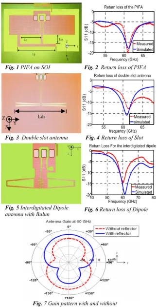
This work presents the performance of 0.13 µm Silicon on insulator technology in the design of 60 GHz fully integrated antennas. Three different types of antennas are considered and designed in order to study their ability to radiate efficiently at this frequency using specific IC technology in order to obtain good matching and higher radiation efficiency. A conductor backed coplanar waveguide is used to feed these antennas. The planar inverted F antenna, the slot antenna and the interdigitated dipole antenna show a good return loss and simulated radiation efficiency of 45%, 55% and 88% respectively. Backside substrate metallization has been used to improve radiation properties.
Introduction
With increasing use of coplanar waveguide (CPW) for MMIC’s, particularly at millimeter frequencies, there is a need for a complete family of compatible planar printed antennas. CPW fed antenna have received considerable attention recently, [1] due to the low radiation loss and less dispersion of the CPW transmission line (TL) with respect to microstrip TL. Recently, Silicon on Insulator (SOI) technology was found to offer alternative solutions to many problems faced in the race to higher performance and low power of integrated devices [2] . CMOS-bulk technologies use low resistivity silicon substrates that, at high frequency, drastically increase the losses in/around antenna and active devices. Furthermore, the use of low resistivity substrates increases the cross-talk between the noisy digital circuits and the sensitive analog radiofrequency (RF) part. SOI offer the opportunity to design integrated circuits on high resistivity substrates leading to reduced losses as well as improved substrate insulation [3]. A 60 GHz band is an attractive candidate for short range radar and indoor communications based on Pico cell zone because it presents high atmospheric loss. The design of integrated antennas operating at 60 GHz is a critical issue when high efficiency is required. In this paper, we propose different design of antennas integrated on SOI, notably a planar inverted-F antenna, a slot antenna and a dipole antenna incorporating an interdigitated structure used to assure good matching impedance with 50 ohm input. The three antennas are fed by CPW TL to be compatible with RF pads. The antennas were simulated using the commercial MWS CST software.
Antenna and Design Configuration
The length of the antenna is inversely proportional to the frequency of operation and the effective permittivity of the substrate on which the antenna is integrated. Using high permittivity materials like silicon and operating at high frequency (60 GHz) will decrease the length of the antenna and hence the overall substrate surface. The topology of SOI substrate is as follows: a high resistive silicon layer (>1000 ohm.cm), six metals layers, buried oxide layer and finally a passivation layer. To assure a 50 ohms feeding to the antenna, CPW TL is designed and characterized for subsequent de-embedding procedure. Three types of antennas are designed, based on electromagnetic simulation, and measured using a HP8510 vector network analyzer. Antennas are etched on the sixth layers of SOI substrate.
1. PIFA antenna
The planar inverted F antenna (PIFA) (Fig. 1) is fed by a CPW TL whose ground planes (M6 layer) are connected by underpaths (M1 layer) through vias to suppress unwanted modes propagation. The return loss (S11 dB) is optimized by adjusting the parameters of antenna. Here, the parameters are Lcp, Lp, and Lc and the width of the radiating arms. The final values of antenna dimension with respect to guided wavelength are showed by the following expressionsLp=0.25λg =622µm,Lcp=0.06λg,Lc=0.136λg.
2. Double slot antenna.
The length of this antenna (Fig. 3) Lds controls the frequency of resonance. The role of the number of slot is to decrease the input impedance of antenna. In fact, using Babinet’s principle, an N-element slot antenna has input impedance given by
2
, Z N
ZinN = slot where
slot
Z is the input impedance of a single slot antenna
(≈500 Ω in free space). The widths of insider slots are cautionary chosen in order to have a good matching with 50 Ohms feed. The arms are short circuited to increase the operational bandwidth.
3. Interdigitated Dipole antenna
The third type of antenna is the most conventional antenna: the dipole antenna. To compensate the substrate effect on the input impedance, a combination of techniques is directly implemented inside the dipole structure (Fig. 5). In the first step, the arm width is
hal-00193727, version 1 - 4 Dec 2007
increased to reduce the quality factor of resonance and obtain a wider operating bandwidth. In the second step, we take advantage of wide arms of the dipole to introduce an interdigitated capacitor [2] in order to mainly decrease the imaginary part of the input impedance. In addition to decrease the input reactance of the antenna, this interdigitated structure affects also its input resistance. A CPW to CPS transition circuit was designed to transform the unbalanced CPW feed line to a balanced CPS (balun) feed line in order to optimize the input of the balanced antenna [2].The final 60 GHz fully integrated dipole antenna incorporating the interdigitated capacitor is realized on 0.13 µm SOI process, with following parameters: Dipole’s length = 742 µm, width = 100 µm, width of the inter digit =6.25 µm. The arms of the dipole were hollowed out for technological reasons.
The second criterion for the design of compact integrated antenna is the radiation efficiency. Using CMOS bulk technology, the antennas shows high losses and consequently low radiation efficiency. In this article, the antennas are presented from the lowest to the highest efficient antenna. The simulated efficiency of the PIFA is the poorest (45 %) with a gain of 1 dBi, next the slot antenna occupy larger place and have a good radiation efficiency with 55% with a gain of 3 dBi, and finally the dipole antenna have the highest efficiency on SOI with 88 % of radiation efficiency with a 4.5 dBi of gain. The lowest order surface wave mode (TM0) has a zero cutoff frequency, and thus is excited to some degree even on very thin substrates. As the substrate becomes thicker, more surface wave modes can exist, and more power can be coupled into these waves and consequently more losses are obtained. The simulated radiation pattern of these antennas is mainly directed toward the SOI substrate. With a backside metallization, the radiation pattern is the directed outward the substrate (Fig. 7). The distance between radiating arms and the reflector (355µm~λg 4) is close to the optimal distance
to prevent TM mode which reduces radiation efficiency [4].
Experimental results and discussion
The three antennas were characterized experimentally using a HP 8510 XF vector network analyzer (VNA). For the PIFA, Fig. 2 shows the comparison of the measured and simulated return loss. The return loss is 18 dB with a bandwidth of 2 GHz for -9.54 dB limit. For the Slot antenna, the measured and simulated return loss of the full antenna with the CBCPW feeding is showed in Fig. 4. The double slot antenna exhibits 2 GHz of bandwidth at -10 dB. The TRL calibration technique was used to extract the intrinsic return loss of the slot antenna without the feeding. Finally, the interdigitated dipole shows better results with a 15 dB return loss at 60 GHz with an 8%
bandwidth (Fig. 6). Measurements of antenna gain and radiation pattern are on the way.
Conclusion
This paper has presented the design and preliminary measurement results for 60 GHz set of antenna integrated on SOI. The results show good correspondence between the measured and simulated return loss. Simulated radiation efficiency shows the importance of SOI technology in the antenna design. These antennas are co-designed with an integrated Low Noise Amplifier in CMOS SOI technology for an RF Front End at 60 GHz.
Reference
[1] Kim, Y. et al, E.L., Vol. 40, Issue 7, P403-405, April 2004. [2] M.H. Barakat et al,”, 2007 IEEE APS, June 2007 [3] C. Tinella, et al, (ESSCIRC), Florence, Italy, 2002. [4] D. M. Pozar,,IEEE Trans. APS, Vol. AP-31, No 5, Sep. 1983.
55 60 65 -20 -15 -10 -5 0
Return loss of the PIFA
Frequency (GHz) S 1 1 ( d B ) Measured Simulated 55 60 65 -20 -15 -10 -5 0
Return loss of double slot antenna
frequency (GHz) S 1 1 ( d B ) Measured simulated 40 50 60 70 80 -20 -15 -10 -5 0
Return Loss For the interdigitated dipole
Frequency (GHz) S 1 1 ( d B ) Measured Simulated Lds Y X Z
Fig. 7 Gain pattern with and without reflector for interdigitated dipole Fig. 5 Interdigitated Dipole
antenna with Balun Fig. 6 Return loss of Dipole Fig. 4Return loss of Slot Fig. 3 Double slot antenna
Fig. 2 Return loss of PIFA Fig. 1 PIFA on SOI