HAL Id: hal-03183877
https://hal.archives-ouvertes.fr/hal-03183877
Submitted on 29 Mar 2021
HAL is a multi-disciplinary open access
archive for the deposit and dissemination of
sci-entific research documents, whether they are
pub-lished or not. The documents may come from
teaching and research institutions in France or
abroad, or from public or private research centers.
L’archive ouverte pluridisciplinaire HAL, est
destinée au dépôt et à la diffusion de documents
scientifiques de niveau recherche, publiés ou non,
émanant des établissements d’enseignement et de
recherche français ou étrangers, des laboratoires
publics ou privés.
substrate
Alban Gassenq, Etienne Cleyet-Merle, Hoshang Sahib, Bruno Baguenard, Ali
Belarouci, Régis Orobtchouk, Frederic Lerouge, Stephan Guy, Antonio Pereira
To cite this version:
Alban Gassenq, Etienne Cleyet-Merle, Hoshang Sahib, Bruno Baguenard, Ali Belarouci, et al..
Rare-earth doped micro-emitters made by lift-off processing in pulsed laser deposited layers on Si
sub-strate. Optics Express, Optical Society of America - OSA Publishing, 2021, 29 (5), pp.7321-7326.
�10.1364/oe.416450�. �hal-03183877�
Rare-earth doped micro-emitters made by lift-off
processing in pulsed laser deposited layers on
Si substrate
A
LBANG
ASSENQ,
1,*E
TIENNEC
LEYET-M
ERLE,
1H
OSHANGS
AHIB,
1B
RUNOB
AGUENARD,
1A
LIB
ELAROUCI,
2R
ÉGISO
ROBTCHOUK,
2F
REDERICL
EROUGE,
3S
TEPHANG
UY,
1 ANDA
NTONIOP
EREIRA11Université de Lyon, Institut Lumière Matière, UCBL, CNRS, UMR5306, F-69622, LYON, France 2Institut des Nanotechnologies de Lyon, Ecole Centrale de Lyon, CNRS, INSA, UCBL, UMR 5270, F-69134
Ecully, France
3Université de Lyon, Laboratoire de Chimie, Ecole Normale Supérieure de Lyon, CNRS, UCBL, UMR5182,
F-69364 Lyon, France
Abstract: Rare earth emitters are promising in integrated optics but require complex integration on silicon. In this work, we have fabricated an Y2O3:Eu3+ micro-emitter on SiO2 on Si substrate without etching. Since pulsed laser deposition produces a high quality layer at room temperature, material can be locally deposited on top of substrates by lift-off processing. After annealing, microstructures exhibit good crystallographic quality with controlled dimensions for light confinement and narrow emission. This works allows envisioning rare-earth doped micro-photonic structures directly integrated on silicon without etching, which opens the way to integration of new functional materials on silicon platform.
© 2021 Optical Society of America under the terms of theOSA Open Access Publishing Agreement
1. Introduction
Rare earth emitters have been studied for a while in integrated optics as laser source [1] and waveguide amplifier with glasses [2,3] or polymer [4]. Recently, they have been integrated in Complementary Metal Oxide Semiconductor (CMOS) driven or compatible Si photonics chip as active devices like laser sources [5], amplifiers [6,7] as well as modulators [8,9]. Rare earth emitters offer thus many possibilities for developing new active functions in integrated optics initially focused on group IV [10] or III-V materials [11,12]. However, complex processing is needed for their efficient incorporation on silicon platform such as bonding [13], masked deposition [5,14], additional layer [15], or etching [16,17] which can be costly and detrimental for practical applications. This is especially the case for Y2O3and Al2O3matrix which require inductively coupled plasma optimized etching [18–20].
In this work, we propose an innovative design of rare-earth doped layer micro-emitters without etching using lift-off processing combined with Pulsed Laser Deposition (PLD). While the classical structuring via etching is performed with the partial erosion of a full-surface coating of the substrate through a mask (e. g. photoresist), in the lift-off procedure, the material is cleared away with the structured resist together with the material deposited thereon. Such method is easier than etching and avoids potential damage along the etched sidewall. Lift-off processing is conventional in microelectronics for thin layer patterning (e.g metal) or thicker layer with low temperature deposition like sputtering [21], atomic layer [22], or glass deposition [23]. Although very attractive, one of the main drawbacks of the lift-off procedure is the substrate temperature during deposition. Indeed, if the substrate temperature is higher than 200°C (i.e the hard bake temperature of the photoresist), lift-off processing cannot be successful. PLD allows overcoming such limitation. PLD is a high quality growth technique commonly used for many applications in
#416450 https://doi.org/10.1364/OE.416450
photonics [24] which can provide for instance low loss waveguide grown at room temperature [25]. One of the main advantages of PLD lies on the fact that the atoms/molecules reaching the surface during deposition have a kinetic energy which exceeds the thermal energy by several orders of magnitude [26]. Such phenomenon leads to the possibility to grow films on substrates in a range of temperatures much lower than otherwise required with other technics (Molecular Beam Epitaxy, Chemical Vapor Deposition. . . ). Therefore, the possibility to merge both technologies (i.e lift-off and PLD) is of great interest for the direct integration of structures for photonics applications.
In this paper, we focus on the fabrication and the study of micro-structured Y2O3:Eu3+layers to demonstrate light confinement and emission without etching. We first have investigated planar Y2O3:Eu3+layers. X-Ray Diffraction (XRD) and Photoluminescence (PL) measurements were performed directly after room temperature deposition and compared with samples annealed at 650°C. We have then fabricated Y2O3:Eu3+microstructures on SiO2buffer layers deposited on Si substrate. As a function of the waveguide width, we have observed different confined modes compared with modeling. Finally, we have performed PL measurements showing a strong emission of the micro-emitters.
2. Pulsed laser deposited Y2O3:Eu3+planar layers
Y2O3:Eu3+is a material of choice for integrated optics. The Eu3+ion is well known for its intense red emission under UV excitation and for its quantum yield close to 100% [27] which could be very interesting for visible integrated optic [28]. Moreover, Y2O3host presents many advantages. Yttrium Oxide has a large band gap which ensures optical transparency for a wide range of wavelengths and it is chemically stable. Furthermore the atomic radius of Yttrium and Europium are in the same range which allows an efficient rare earth incorporation [29]. Y2O3:Eu3+300 nm planar layers were first deposited on SiO2(2 µm)/Si substrate. A KrF excimer laser (λ=248 nm, t=17 ns, Coherent Compex Pro) operating at 5 Hz was used for the ablation of the target under 73 mJ, focused over 2mm2. Substrate rotation was used to obtain homogeneous layer thickness at the growth speed of 3.5 nm/min, at room temperature in an oxygen-gas atmosphere (10−3mbar). The distance between the sample and the Y2O3:Eu3+target was set to 6 cm. After the growth, samples were annealed 24 hours at 650°C with a 0.5°C/min ramp under ambient air. Figure1 presents XRD and PL measurements before and after annealing. X-ray diffraction (XRD) patterns were collected using a D2-phaser Bruker instrument with Cu- Kα radiation (λ = 0.1540598 nm)
Fig. 1.Y2O3:Eu3+layer before and after annealing compared by a) X-ray diffraction and a) photoluminescence measurement with the excitation spectra presented in the inset
using a graphite monochromator in the 2θ range from 25 to 55° [Fig.1(a)]. Before annealing, no pics are detected which evidence the amorphous character of the Y2O3thin film. After annealing, the XRD pattern shows that all diffraction peaks can be indexed to the Y2O3cubic phase (JCPDS 00-041-1105) and no signal from another phase (Y2O3monoclinic) or impurities is observed, indicating that the product is single-phase [30,31]. PL measurements were performed with an Oriel Cornerstone CS260 monochromator and a Hamamatsu R1477 visible photo-multiplier. Roithner LED UVR270SC3P pump source was focused over few mm2with a centered wavelength around 270 nm. The excitation spectrum is highlighted on the inset of Fig.1(b). This excitation wavelength corresponds to the excitation of the Eu-O charge band [32,33]. Light emission is then collected from ∼mm2surface aligned with the pumped region. Without annealing, Y2O3:Eu3+ emission spectrum is broad with low intensity, due to the amorphous Y2O3matrix [34]. Note that rare earth emission is nevertheless detected with such low temperature deposition which could be interesting for CMOS compatible applications. After annealing, we clearly see that narrow and higher intensity emission bands are detected, corresponding to the well-known Eu3+energy level in a crystalline Y2O3host [32,35]. Therefore, our growth conditions allow depositing Y2O3:Eu3+ layers with enhanced emission properties after annealing, as expected [34].
Layer thickness and refractive index were measured before and after annealing using a Dektak profilometer and a J.A Woollan Ellipsometer. A good correlation was found between both measurements. Before annealing, the layer thickness was estimated to be 0.30 µm and 0.28 µm after annealing. Furthermore, the refractive index increases from 1.80 to 1.87 at 610 nm wavelength (seeSupplement 1). Such measurements indicate that the layer density increases
during the annealing step, as previously reported in the literature [36–38]. 3. Processing for micro-structuration
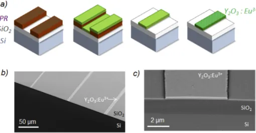
Figure2(a) reports the process flow for the Y2O3:Eu3+micro-structuration. AZ5214 negative photoresist ]PR in the Fig.2(a)] was used on top of a 2 µm thermal SiO2buffer on Si substrate. UV lithography was achieved with a standard EVG mask aligner and standard Cr lithography photomask. 1.8 µm height photoresist strip with 2, 4 and 8 µm width were defined along the <110> Si crystalline axis. Afterward, samples were directly placed under vacuum to prevent
Fig. 2.a) Process flow for the rare-earth based micro-emitters starting by UV lithography, followed by Y2O3 deposition, lift-off and 650°C annealing; b) Tilted SEM imaging of micro-structured Eu3+doped Y2O3layers showing different waveguide width and c) zoom in the cross-section
photoresist drying. PLD was then carried out under the same experimental conditions as described in the previous section for 0.3 and 0.6 µm layer thicknesses. Subsequently, samples were immersed in acetone and placed into an ultrasonic bath. During this process step, since the material is only deposited on the SiO2surface at specific locations which are not protected by a resist mask, the subsequent lift-off clears away the resist structures together with the material deposited thereon, while the material directly deposited on the substrate through the openings of the resist mask remains there, as desired. Finally, samples were annealed in air for 24 hours at 650°C with a 0.5°/min ramp. Figures2(b) and2(c) present Scanning Electron Microscopy (SEM) images of samples cleaved along the <-110> Si crystalline axis and tilted at 45°. For these observations, samples were metalized with 5 nm thick Pt/Pd layer to circumvent charging effects. In Fig.2(b), the black region corresponds to the Si substrate, the grey to SiO2, and the white strips to the Y2O3:Eu3+. In Fig.2(c), the darker grey region corresponds to the SiO2buffer and the brighter region is the Y2O3:Eu3+, as indicated in the Figures. We clearly see that the waveguide width can be controlled by the lithography step [Fig.2(b)] with a nice cross-section after annealing [Fig.2(c)]. Note that, sidewall roughness could be improved by optimizing the lithography and deposition steps.
4. Optical characterizations
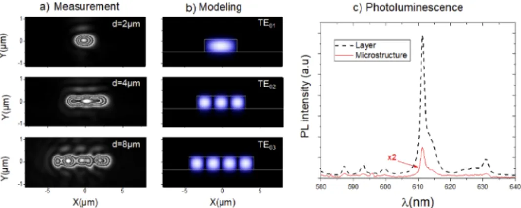
In order to measure light confinement in such waveguide, mode profile intensity was measured for different waveguide widths. For that purpose, a 635 nm wavelength fiber-coupled laser light (Roithner Laser Technik) is coupled/decoupled to the film waveguide with x20 microscope objectives (numerical aperture 0.4). Since Y2O3is cubic polycrystalline, high losses (>dB/mm) were detected in the structured waveguides as well as in planar layers (i.e unstructured layers). Therefore, 2 mm length waveguides were studied to have enough intensity to measure the mode profile at the output with a CCD camera (Stingray F201B). Note that such materials losses could be improved by optimizing Y2O3temperature growth [39] or by using Al2O3host [40,41]. Figure3(a) presents examples of 3 modes profile captured for a 0.6 µm-thick waveguide with 2, 4 or 8 µm widths. We clearly see that different propagated modes can be observed as a function of the waveguide width. In this measurement, we have chosen to evidence the multimode behavior in the largest waveguide by adjusting the input light at the waveguide entrance. For comparison, modeling by SIIO mode solver [42] was computed with a refractive index of 1.45 for SiO2[43] and 1.87 for Y2O3according to ellipsometric measurement (seeSupplement 1). According to
Fig. 3. Optical characterization of a 0.6 µm-thick micro-structured Y2O3:Eu3+ layer for mode profile at 610 nm wavelength: a) measured and b) simulated intensity. c) Photoluminescence of micro-structured Y2O3:Eu3+layer compared to planar layers
modeling, multimode propagation is confirmed [Fig.3(b)]. Therefore, we highlight here that the electromagnetic field is well confined in the microstructure alloying to control light propagation.
Finally, PL measurements were performed on micro-structured samples compared to un-structured layers with the same measurement setup presented previously. Figure3(c) presents the emission spectra. We find a PL intensity reduction factor of around 10, which is close to the Y2O3:Eu3+surface ratio between the structured and the unstructured samples. Furthermore, the PL spectra shape is similar between single layers and which confirms that the micro-structuration does not affect significantly the layer quality.
5. Conclusion
In this work, we have demonstrated the possibility to fabricate Y2O3:Eu3+micro-emitters without etching allowing light emission and confinement. We have first studied the photoluminescence of Y2O3:Eu3+planar layers showing good crystalline quality and strong emission after annealing. We have then fabricated micro-structured Y2O3:Eu3+strip on SiO2layers on Si showing multimode light confinement. Finally, we have performed photoluminescence measurements which exhibit intense emission of the micro-structured layers. This work opens a way to the fast integration of rare-earth micro-emitters directly in photonics chip without etching processing, and thus for the integration of new functional materials on silicon platforms.
Acknowledgements.The authors would like to thank the NanoLyon platform for the cleanroom facilities. Disclosures.The authors declare no conflicts of interest.
Supplemental document.SeeSupplement 1for supporting content. References
1. J. H. Park and A. J. Steckl, “Demonstration of a visible laser on silicon using Eu-doped GaN thin films,”J. Appl. Phys.98(5), 056108 (2005).
2. E. Lallier, “Rare-earth-doped glass and LiNbO_3 waveguide lasers and optical amplifiers,”Appl. Opt.31(25), 5276 (1992).
3. K. J. Malone, “Integrated optical devices in rare-earth-doped glass,”Glas. Integr. Opt. Opt. Fiber Devices A Crit. Rev.10275, 1027509 (1994).
4. E. Y. B. Pun, “Rare earth doped polymeric integrated optical devices,” Opt. InfoBase Conf. Pap., 2000–2002 (2006). 5. N. Li, M. Xin, Z. Su, E. S. Magden, N. Singh, J. Notaros, E. Timurdogan, P. Purnawirman, J. D. B. Bradley, and M.
R. Watts, “A Silicon Photonic Data Link with a Monolithic Erbium-Doped Laser,”Sci. Rep.10(1), 1–9 (2020). 6. J. Rönn, W. Zhang, A. Autere, X. Leroux, L. Pakarinen, C. Alonso-Ramos, A. Säynätjoki, H. Lipsanen, L. Vivien, E.
Cassan, and Z. Sun, “Ultra-high on-chip optical gain in erbium-based hybrid slot waveguides,”Nat. Commun.10(1), 432–439 (2019).
7. P. Xing, G. F. R. Chen, X. Zhao, D. K. T. Ng, M. C. Tan, and D. T. H. Tan, “Silicon rich nitride ring resonators for rare-earth doped telecommunications-band amplifiers pumped at the O-band,”Sci. Rep.7(1), 1–9 (2017). 8. C. Wang, M. Zhang, B. Stern, M. Lipson, and M. Lončar, “Nanophotonic lithium niobate electro-optic modulators,”
Opt. Express26(2), 1547 (2018).
9. X. Jiang, D. Pak, A. Nandi, Y. Xuan, and M. Hosseini, “Rare earth-implanted lithium niobate: Properties and on-chip integration,”Appl. Phys. Lett.115(7), 071104 (2019).
10. N. Von Den Driesch, D. Stange, S. Wirths, G. Mussler, B. Holländer, Z. Ikonic, J. M. Hartmann, T. Stoica, S. Mantl, D. Grützmacher, and D. Buca, “Direct Bandgap Group IV Epitaxy on Si for Laser Applications,”Chem. Mater.
27(13), 4693–4702 (2015).
11. S. Chen, W. Li, J. Wu, Q. Jiang, M. Tang, S. Shutts, S. N. Elliott, A. Sobiesierski, A. J. Seeds, I. Ross, P. M. Smowton, and H. Liu, “Electrically pumped continuous-wave III–V quantum dot lasers on silicon,”Nat. Photonics10(5), 307–311 (2016).
12. Z. Wang, B. Tian, M. Pantouvaki, W. Guo, P. Absil, J. Van Campenhout, C. Merckling, and D. Van Thourhout, “Room Temperature InP DFB Laser Array Directly Grown on (001) Silicon,”Nat. Photonics9(12), 837–842 (2015). 13. X. Jiang, D. Pak, A. Nandi, Y. Xuan, and M. Hosseini, “Rare earth-implanted lithium niobate: Properties and on-chip
integration,”Appl. Phys. Lett.115(7), 071104 (2019).
14. R. W. Eason, T. C. May-Smith, C. Grivas, M. S. B. Darby, D. P. Shepherd, and R. Gazia, “Current state-of-the-art of pulsed laser deposition of optical waveguide structures: Existing capabilities and future trends,”Appl. Surf. Sci.
255(10), 5199–5205 (2009).
15. N. V. Hoang, A. Pereira, H. S. Nguyen, E. Drouard, B. Moine, T. Deschamps, R. Orobtchouk, A. Pillonnet, and C. Seassal, “Giant Enhancement of Luminescence Down-Shifting by a Doubly Resonant Rare-Earth-Doped Photonic Metastructure,”ACS Photonics4(7), 1705–1712 (2017).
16. L. Agazzi, J. D. B. Bradley, M. Dijkstra, F. Ay, G. Roelkens, R. Baets, K. Wörhoff, and M. Pollnau, “Monolithic integration of erbium-doped amplifiers with silicon-on-insulator waveguides,”Opt. Express18(26), 27703 (2010). 17. S. Dutta, E. A. Goldschmidt, S. Barik, U. Saha, and E. Waks, “Integrated Photonic Platform for Rare-Earth Ions in
Thin Film Lithium Niobate,”Nano Lett.20(1), 741–747 (2020).
18. J. D. B. Bradley, F. Ay, K. Wörhoff, and M. Pollnau, “Fabrication of low-loss channel waveguides in Al2O3 and Y2O3 layers by inductively coupled plasma reactive ion etching,”Appl. Phys. B89(2-3), 311–318 (2007). 19. Y. C. Cao, L. Zhao, J. Luo, K. Wang, B. P. Zhang, H. Yokota, Y. Ito, and J. F. Li, “Plasma etching behavior of Y2O3
ceramics: Comparative study with Al2O3,”Appl. Surf. Sci.366, 304–309 (2016).
20. K. Wörhoff, J. D. B. Bradley, F. Ay, D. Geskus, T. P. Blauwendraat, and M. Pollnau, “Reliable low-cost fabrication of low-loss Al2O3:Er3+ waveguides with 5.4-dB optical gain,”IEEE J. Quantum Electron.45(5), 454–461 (2009). 21. T. Yachi and T. Serikawa, “Lift-Off Patterning of Sputtered SiO2 Films (LOPAS) and Its Application to Recessed
Field Isolation,”J. Electrochem. Soc.132(11), 2775–2778 (1985).
22. J. Biercuk, D. J. Monsma, C. M. Marcus, J. S. Becker, and R. G. Gordon, “A Low-Temperature Atomic Layer Deposition Liftoff Method for Microelectronic and Nanoelectronic Applications M,”Appl. Phys. Lett.83(12), 2405–2407 (2003).
23. J. Hu, V. Tarasov, N. Carlie, N.-N. Feng, L. Petit, A. Agarwal, K. Richardson, and L. Kimerling, “Si-CMOS-compatible lift-off fabrication of low-loss planar chalcogenide waveguides,”Opt. Express15(19), 11798 (2007).
24. R. Eason, Pulsed Laser Deposition of Thin Films: Applications-Led Growth of Functional Materials (Wiley-Interscience, New Jersey, 2006).
25. M. Jelínek, “Growth of optical waveguides by pulsed laser deposition,”Laser Phys.19(2), 265–273 (2009). 26. D. H. Lowndes, Laser Ablation and Desorption, Exp. Metho (Academic, New York, 1998).
27. K. Binnemans, “Interpretation of europium(III) spectra,”Coord. Chem. Rev.295, 1–45 (2015).
28. P. Muñoz, G. Micó, L. A. Bru, D. Pastor, D. Pérez, J. D. Doménech, J. Fernández, R. Baños, B. Gargallo, R. Alemany, A. M. Sánchez, J. M. Cirera, R. Mas, and C. Domínguez, “Silicon nitride photonic integration platforms for visible, near-infrared and mid-infrared applications,”Sensors17(9), 2088 (2017).
29. S. Agrawal and V. Dubey, “Down conversion luminescence behavior of Er and Yb doped Y 2 O 3 phosphor,”J. Radiat. Res. Appl. Sci.7(4), 601–606 (2014).
30. Y. Xie, L. Wang, B. Liu, L. Zhu, S. Shi, and X. Wang, “Flexible, controllable, and high-strength near-infrared reflective Y2O3 nanofiber membrane by electrospinning a polyacetylacetone-yttrium precursor,”Mater. Des.160, 918–925 (2018).
31. P. Zhang, A. Navrotsky, B. Guo, I. Kennedy, A. N. Clark, C. Lesher, and Q. Liu, “Energetics of cubic and monoclinic yttrium oxide polymorphs: Phase transitions, surface enthalpies, and stability at the nanoscale,”J. Phys. Chem. C
112(4), 932–938 (2008).
32. N. Abdellaoui, A. Pereira, T. Kandri, E. Drouard, M. Novotny, B. Moine, and A. Pillonnet, “Luminescence enhancement of a self-organised Y2O3:Eu3+ thin film-coated porous alumina membrane,”J. Mater. Chem. C4(39), 9212–9218 (2016).
33. N. Abdellaoui, A. Pillonnet, J. Berndt, C. Boulmer-Leborgne, E. Kovacevic, B. Moine, J. Penuelas, and A. Pereira, “Plasmonic enhancement of Eu:Y2O3 luminescence by Al percolated layer,”Nanotechnology26(9), 095701 (2015). 34. M. Scarafagio, A. Tallaire, K. Tielrooij, D. Cano, A. Grishin, M. Chavanne, F. Koppens, A. Ringuede, M. Cassir, D. Serrano, M. Scarafagio, A. Tallaire, K. Tielrooij, D. Cano, and A. Grishin, “Ultrathin Eu- and Er-Doped Y2O3 Films with Optimized Optical Properties for Quantum Technologies,”J. Phys. Chem. C123(21), 13354–13364 (2019). 35. L. Ji, N. Chen, G. Du, M. Yan, and W. Shi, “Synthesis and luminescence of Y2O3:Eu3+ inorganic-organic hybrid
nanostructures with thenoyltrifluoroacetone,”Ceram. Int.40(2), 3117–3122 (2014).
36. M. H. Tang, Y. C. Zhou, X. J. Zheng, Z. Yan, C. P. Cheng, Z. Ye, and Z. S. Hu, “Characterization of ultra-thin Y2O3 films as insulator of MFISFET structure,”Trans. Nonferrous Met. Soc. China16(Supplement 1), s63–s66 (2006). 37. A. D. J. Morales Ramírez, A. García Murillo, F. D. J. Carrillo Romo, M. García Hernández, E. De La Rosa, and
J. Moreno Palmerin, “Y2O3:Eu3+,Tb3+ thin films prepared by sol-gel method: Structural and optical studies,”J. Sol-Gel Sci. Technol.58(2), 366–373 (2011).
38. J. Serafin, T. Wiktorczyk, and P. Biegan, “Optical properties of nanocrystalline Y2O3 thin films grown on quartz substrates by electron beam deposition,”Opt. Mater.59, 150–156 (2016).
39. J. W. Szela, K. A. Sloyan, T. L. Parsonage, J. I. Mackenzie, and R. W. Eason, “Laser operation of a Tm:Y2O3 planar waveguide,”Opt. Express21(10), 12460 (2013).
40. A. Suárez-García, J. Gonzalo, and C. N. Afonso, “Low-loss Al2O3 waveguides produced by pulsed laser deposition at room temperature,”Appl. Phys. A: Mater. Sci. Process.77(6), 779–783 (2003).
41. Y. Yang, B. Wang, A. Cormack, E. Zych, H. J. Seo, and Y. Wu, “Theoretical analysis and experiment on Eu reduction in alumina optical materials,”Opt. Mater. Express6(7), 2404 (2016).
42. “SIIO mode solver,”https://www.siio.eu/eims.html.
43. I. H. Malitson, “Interspecimen Comparison of the Refractive Index of Fused Silica,”J. Opt. Soc. Am.55(10), 1205 (1965).