Diastolic Arrays: Throughput-Driven
Reconfigurable Computing
by
Myong Hyon Cho
Submitted to the Department of Electrical Engineering and Computer
Science
in partial fulfillment of the requirements for the degree of
Master of Science in Electrical Engineering and Computer Science
at the
MASSACHUSETTS INSTITUTE OF
IMay 2008o3
May 2008
TECHNOLOGY
@ Massachusetts Institute of Technology 2008. All rights reserved.
Author.
Department of Electrical Engineering and Computer Science
May 20, 2008
C ertified by ...
...
Srinivas Devadas
Professor of Electrical Engineering and Computer Science
Thesis Supervisor
Accepted by
MASSACHUSETTS INSTITUE OF TEOHNOLOGYJUL 0 1 2008
LIBRARIES
Arthur C. Smith
Chairman, Department Committee on Graduate Students
Diastolic Arrays: Throughput-Driven Reconfigurable
Computing
by
Myong Hyon Cho
Submitted to the Department of Electrical Engineering and Computer Science on May 20, 2008, in partial fulfillment of the
requirements for the degree of
Master of Science in Electrical Engineering and Computer Science
Abstract
In this thesis, we propose a new reconfigurable computer substrate: diastolic ar-rays. Diastolic arrays are arrays of processing elements that communicate exclusively through First-In First-Out (FIFO) queues, and provide hardware support to guar-antee bandwidth and buffer space for all data transfers. FIFO control implies that a module idles if its input FIFOs are empty, and stalls if its output FIFOs are full. The timing of data transfers between processing elements in diastolic arrays is there-fore significantly more relaxed than in systolic arrays or pipelines. All specified data transfers are statically routed, and the routing problem to maximize average through-put can be optimally or near-optimally solved in polynomial time by formulating it as a maximum concurrent multicommodity flow problem and using linear program-ming. We show that the architecture of diastolic arrays enables efficient synthesis from high-level specifications of communicating finite state machines, providing a high-performance, off-the-shelf computer substrate that can be easily programmed. Thesis Supervisor: Srinivas Devadas
Acknowledgments
First, I would like to express my sincere gratitude to Professor Srinivas Devadas for his extraordinary guidance and support throughout this research. His great insight has always inspired me and with his supervision I have never felt like I was lost. I also thank Professor Edward Suh who have so kindly helped me in this research as well as in every aspects of my graduate life. I thank Joel Emer, Vijay Ganesh, Mieszko Lis, Michael Pellauer, Bill Thies and David Wentzlaff for helpful comments on this research.
I also would like to thank all of Computation Structures Group people. I greatly thank Chih-chi Cheng for his help in application experiments and Michel Kinsy for the simulator development, and above all, for their being good friends. I send my heartfelt gratitude to Charles O'Donnell who helped me find everything I need, Alfred Ng and Murali Vijayaraghavan who gave me wonderful feedback, and Jaewook Lee who has been my mentor in graduate school. I warmly thank Mieszko Lis again, this time for greeting me everytime in Korean language.
I cannot thank enough to my parents and family who always helped me in every possible way. I truly thank them for their encouragement and their love. I also thank all of my friend, especially my girl friend Myunghee who has always been by my side even from the other side of the planet. Last but not least, I would like to extend my special gratitude to Samsung Scholarship who financially supported me during my master study.
Contents
1 Introduction
2 Background and Related Work
2.1 Computing Substrates . ...
2.2 Interconnection Network and Multi-commodity Flow Problem . . .
3 Motivating Applications
3.1 Computational Model ...
3.2 Example: H.264 Decoder ... 3.3 Example: Performance Modeling 3.4 Other Applications ...
4 Diastolic Architecture
4.1 Microarchitecture Overview ... 4.2 PE and PE-to-PFIFO Interface ... 4.3 Physical FIFOs (PFIFOs) . ...
4.3.1 Buffer Allocation for Virtual.FIFOs ... 4.3.2 Scheduling for Composite-path Routes ...
4.3.3 Arbitration of VFIFOs with the Same Destination . 4.3.4 Data Reception Protocol ...
4.4 Performance Optimization: Timestamp . ... 4.5 Diastolic Architecture Simulator ...
23 .. . . . . . . 23 .. . . . . 24 .. . . . . . . . 27 .. . . . . 28 29 . . . . . . 30 . . . . . . 31 . . . . . . 32 . . . . . . 32 . . . . . . 33 . . . . . . 34 . . . . . . 34 .. . . . 35 . . . . . . 37
5.2 5.3 5.4 5.5 5.6 5.7 5.8 5.9 6 Experimental Results 6.1 H.264 Decoder ...
6.2 Processor Performance Modeling ...
7 Conclusion and Future Directions 5 Synthesis Flow 5.1 Synthesis Overview 39 39 Application Specification .. ... Profiling ... 5.3.1 High-level Profiling ... 5.3.2 Bandwidth Profiling ... 5.3.3 Buffer Profiling ...
Module Grouping and Partitioning ... PE Compilation ...
PE Placement ...
Routing and Buffer Allocation of Virtual FIFOs
5.7.1 Multi-commodity Flow Linear Program .
5.7.2 Buffer Allocation Linear Program ....
5.7.3 Alternative Routing Algorithms ... Configuration ...
Minimizing Latency of Virtual FIFOs ...
-List of Figures
3-1 High-level Module Description of H.264 Decoder . ... 24
3-2 FIFO size vs. Data Throughput of H.264 Decoder Modules: Entropy
Decoder and Inter-prediction ... .... 26
4-1 A PE Architecture and a Single-path and a Composite-path Route of
a VFIFO ... ... ... ... 30
4-2 The PFIFO to PFIFO Interface ... .. 35
4-3 Optimization through Explicit Synchronization by Timestamp . . .. 37
5-1 Synthesis Flow for Diastolic Arrays . ... 40
5-2 H.264 Specification after Module Group and Partition ... 44
5-3 Configuring Marking and Acknowledgement Algorithms for
Composite-path Routes ... ... 53
6-1 Throughput Demand of each VFIFO in H.264 Decoder ... 56
6-2 Routing results of H.264 decoder for different link bandwidths . . . . 57
6-3 Routing Results of H.264 Decoder for a Different Placement and with
the Link Bandwidth of Figure 6-2(d). ... . ... 58
6-4 Buffer allocation of H.264 decoder for the route of Figure 6-2 (c). . . 59
6-5 Throughput Demand of each VFIFO in Processor Performance Modeling 60
6-6 Synthesis Result of Processor Performance Modeling . ... 61
6-7 Average PE Substrate Cycles per System Cycle and the Maximum and
List of Tables
3.1 Profiling Results of H.264 Decoder Modules for a Standard Input . 25
4.1 Basic Instructions for VFIFO Communication ... 31
5.1 Profiling for the Synthesis for Diastolic Arrays ... ... 42
Chapter 1
Introduction
Many computer substrates have been proposed which share the characteristic of hav-ing two-dimensional arrays of processhav-ing elements interconnected by a routhav-ing fabric. Although having the same characteristic, different architectures show very different area-power-performance tradeoffs because their processing elements and routing fab-rics are very different to each other. At one end of the spectrum, for example, Field Programmable Gate Arrays (FPGAs) have many tens of thousands of computing el-ements that are single-output programmable logic functions interconnected through configurable wires. And at the other end, recent multicore processors have multiple-issue 64-bit processors communicating via high-speed bus interconnect. Other ar-chitectures also use homogeneous and heterogeneous processing elements of varying complexity connected by multifarious on-chip networks.
This thesis proposes a diastolic array system 1 which is a reconfigurable substrate that is meant to serve as a coprocessing platform to speed up applications or parts of applications that are throughput-sensitive and latency-tolerant. We will argue, in this thesis, that various applications such as movie decoders and processor performance modeling can be implemented on diastolic array systems more easily and efficiently than on other computing substrates such as FPGAs and multicore processors.
FPGAs are popular for prototyping applications as well as low-volume production. 1The adjective diastolic is used to refer to the relaxation of the heart between muscle contractions.
Data transfers in diastolic arrays have more relaxed latency requirements than in systolic arrays, hence the name.
They avoid the long turnaround time of an Application-Specific Integrated Circuit (ASIC), but have 10-30X area overhead in relation to ASICs and 3-4X performance overhead [24]. Synthesis to FPGAs is a matter of mapping combinational logic and registers to Configurable Logic Blocks (CLBs), and then performing global routing and detailed routing of potentially millions of wires. Routing a wire from one location to another requires configuration of switchboxes, potentially making wires long and slow. The sheer number of wires and the limited bandwidth of the routing channels exacerbate the routing problem. Synthesis to FPGAs can often fail due to routing congestion even though there are many Configuration Logic Blocks (CLBs) that are unused.
Multicore processors such as Quadcore x86 processors and multicore digital signal processors with hundreds of cores have entered the commercial marketplace. Pro-cessors in multicores are typically connected via high-speed bus interconnect. These multicores can take advantage of thread-level parallelism in web applications or data parallelism in video applications. Processes can be compiled to run mostly inde-pendently on the different cores and to communicate with each other through the high-speed interconnect. However, significant programming effort is required to ex-ploit fine-grained parallelism in these architectures.
On the other hand, diastolic arrays are coarser-grained than FPGAs and data communication is defined through high-level design of applications resulting in a synthesis flow that is simpler than in FPGAs. On the other hand, diastolic arrays are finer-grained than multicores and can exploit parallelism more easily. Data transfers in a diastolic array are all statically routed and are allowed a varying number of clocks depending on the length of, and congestion in, the transfer path comprising a sequence of physical FIFOs. FIFO control implies that a module idles if its input FIFOs are empty, and stalls if its output FIFOs are full. FIFOs (that have room for more than one value) average out data-dependent variances in each module's execution and communication, and the performance of the design will be determined by the module with the maximum average latency, not the worst-case input that causes the longest latency in a module.
To be more specific, a diastolic array has programmable processing elements with a simple ISA, running on a fast substrate clock. Diastolic array processors communicate exclusively through First-In First-Out (FIFO) queues attached to a network 2 , and "physical" FIFOs, the routing logic embedded in each processing element, provide hardware support to guarantee bandwidth and buffer space for all data transfers. The architecture of diastolic arrays enables efficient synthesis from high-level specifications of communicating finite state machines so average throughput is maximized.
To program diastolic arrays, the designer writes high-level specifications of appli-cations that describes FSM modules that manipulate data and which communicate exclusively via FIFOs. During synthesis to diastolic arrays, some FSM modules are grouped or partitioned, and modules are assigned to processing elements (placement) while the FIFOs used for communication between modules, named "virtual" FIFOs, are realized as a sequence of physical FIFOs (routing). Then, modules are compiled into instructions for processing elements (compilation), and the physical FIFOs are statically configured to implement the correct virtual FIFO routing, while guaran-teeing bandwidth and buffer space (configuration). For a class of designs, including acyclic stream computations, given a placement, finding routes for all the virtual FIFOs that produce maximum throughput for the design is a maximum concurrent multi-commodity flow problem. An optimal flow under given hardware bandwidth constraints can be found in polynomial time using linear programming. For gen-eral designs with tight feedback, heuristic routing methods can be used to maximize throughput.
This thesis is structured as follows. First, Chapter 2 briefly summarizes related work in reconfigurable logic and interconnect networks. Case studies in Chapter 3 show that averaging data-dependent variances is critical to achieve high throughput for applications such as H.264 decoding and processor performance modeling, moti-vating a diastolic array architecture. Rather than having pipeline registers separating modules as in conventional designs, the use of FIFOs and associated FIFO control
2
The interconnect architecture can vary; we will focus on mesh networks here. However, our algorithms apply to general network topoligies.
can result in significantly better average-case performance, provided the FIFOs can store a small number of intermediate values. A candidate architecture for a diastolic array is presented in Chapter 4. The synthesis flow is presented in Chapter 5. Chap-ter 6 provides preliminary experimental results on H.264 and processor performance modeling benchmarks. Finally, Chapter 7 draws conclusions.
Chapter 2
Background and Related Work
2.1
Computing Substrates
There has been extensive research into computing substrates such as systolic arrays, network-overlaid FPGAs and other FPGA variants, coarse-grained processing plat-forms, and multicore architectures. Their characteristics and differences to diastolic arrays will be briefly summarized in this section.
Systolic arrays [22, 23] have been used to efficiently run many regular applica-tions such as matrix multiplication. These SIMD processors contain synchronously-operating elements which receive and send data in a highly regular manner through a processor array so that the application works at the slowest rate of processors. To the contrary, the timing of data transfers in MIMD diastolic arrays is much more relaxed than in systolic arrays due to FIFO control and the maximum average performance is attained provided the FIFOs have enough buffer space.
Time-multiplexed and packet-switched networks have been overlaid on FPGAs and tradeoffs in implementing these networks and the performance of these overlaid networks has been studied [20]. Modern FPGAs such as those in the Virtex family from Xilinx have optimized carry chains, XOR Lookup Tables, and other features. Commercial synthesis tools can take advantage of these features to produce better implementations. A diastolic array uses time-multiplexing in the processing elements and interconnect and FIFOs for communication and is therefore significantly different
from FPGAs, while remaining homogeneous, which results in a very different synthesis flow.
In addition, systems like the Xilinx CORE Generator System [38] provide param-eterizable Intellectual Property (IP) cores for Xilinx FPGAs that are optimized for higher density. These cores include DSP functions, memories, storage elements and math functions. The CoWare Signal Processing Worksystem (SPW) [9] tool interfaces with the Xilinx CORE Generator System and this integration enables custom DSP data path development on FPGAs using SPW. Jones [19] presents a time-multiplexed FPGA architecture for logic emulation designed to achieve maximum utilization of silicon area for configuration information and fast mapping, with emulation rate, i.e., performance, being only a minor concern. High density is achieved by providing only one physical logic element, and time-multiplexing configuration information for this logic element to provide several virtual logic blocks. Trimberger [36] also presents time-multiplexed FPGAs, where multiple FPGA configurations are stored in on-chip memory. This inactive on-chip memory is distributed around the chip, and accessible in such a way that the entire configuration of the FPGA can be changed in a single cycle of the memory.
Regarding the granularity of processing elements, many coarse-grained reconfig-urable logics have been proposed. MathStar's Field Programmable Object Arrays (FPOA's) [27] are heterogeneous, medium grain, silicon object arrays with 1GHz in-ternal clock speed and flexible I/O interconnect. FPOAs target high performance DSP and multi-gigabit line-rate data processing and bus bridging applications. There are six or more different types of silicon objects. Each silicon object has a loadable con-figuration map that contains both operation and communication instructions. Other medium or coarse grain processing platforms with a few hundred cores include the eXtreme Processing Platform (XPP) [2] and multicore DSPs from Picochip [12] which facilitates bus-based interconnect. MATRIX [28] is a reconfigurable chip with an ar-ray of 8-bit processing elements working like a dynamically programmable FPGA. The MATRIX network is a hierarchical collection of 8-bit busses as well. Diastolic arrays use a mesh-based routing network with FIFOs rather than using bus-based
interconnect.
While diastolic arrays have some similarity to multicore architectures, they are simpler than commercial multicores or architectures such as Raw [37] and Tilera [13], and also target a smaller class of throughput-sensitive, latency-insensitive applica-tions. Raw uses software to control inter-processor communication and has relatively small FIFOs between processor tiles. Unlike Raw, diastolic arrays allow sharing of physical FIFOs by virtual FIFOs in a non-blocking way for data transfers. Tilera has five different networks that interconnect tiles including a static network, whereas diastolic arrays implement a single logically static network that supports sharing of flows, split flows and buffer allocation.
There are many other multicore systems that have been studied. TRIPS [34] uses significantly larger cores that are 16-issue, and Asynchronous Array of simple Proces-sors (AsAP) [40, 39] is a multicore processor for DSP applications, which primarily targets small DSP applications with short-distance communications. AsAP consists of a 2-D array of simple processors connected through dual-clock FIFOs in a Globally Asynchronous Locally Synchronous (GALS) fashion. The FIFO sizes in AsAP are appreciably smaller than those in diastolic arrays, these FIFOs are mainly used to interface two clock domains and hide communication latencies rather than optimiz-ing average case performance as in diastolic arrays. The main purpose of FIFOs in diastolic arrays is not GALS, but a diastolic array implementation under GALS is
also possible.
Additionally, Synchroscalar [30] groups columns of processors into SIMD arrays, and makes heavy use of statically configurable interconnect that can be used as a bus or similarly to a mesh. Ambric [4] uses a circuit-switched network as opposed to a packet-switched network, to avoid the cost of switches and buffers. Channels are set up by configuring the network much like in a FPGA, and synthesis to the Ambric chip is similar to FPGA synthesis, though significantly faster due to structure provided by the designer [3]. There is a small amount of buffering in the channel, and processors stall if they cannot write into the channel or if there is no data available.
2.2
Interconnection Network and Multi-commodity
Flow Problem
Many types of on-chip interconnect networks have been studied. Dally's virtual chan-nels were introduced to avoid deadlock in multiprocessor interconnection networks [10] and the use of virtual channels for flow control allocates buffer space for virtual channels in a decoupled way from bandwidth allocation [11]. On the other hand, diastolic arrays guarantee bandwidth as well as buffer space in a coupled way, and implement multiple-hop, flow-controlled logical channels. Similarly, iWarp [16] could set up fine-grained, buffered direct paths, but only in a regular systolic topology.
The multicommodity problem is a network flow problem with multiple commodi-ties flowing through the network, with different source and sink nodes, and is solvable in polynomial time using linear programming (LP) [8]. Multicommodity flow has been used for global routing of wires with buffering, e.g., [33], [1]. Multicommodity flow has also been used for physical planning on on-chip interconnect architectures (e.g., [6]), to optimize latencies and power consumption network-on-chip architectures (e.g., [17]), and to explore FPGA routing architectures (e.g., [18]). Multicommodity flow has also been used in internet routing of packets (e.g., [29]) and wireless routing (e.g.,
[5]).
We are using multicommodity flow to determine single-path or composite-path routes for data transfers in an on-chip interconnection network for maximum through-put. Virtual FIFOs in diastolic arrays connect arbitrary pairs of processing elements through physical links shared by multiple virtual FIFOs, making the routing prob-lem with throughput constraints a typical multicommodity flow probprob-lem. The buffer space allocation for a given route is also solvable by using LP.
Numerous approximation schemes that are faster than using LP have been devel-oped, e.g., [26]. Also, multicommodity problems with auxiliary conditions such as unsplittable flow or integer throughput have been studied, e.g., [21]. Our problem usually has significantly fewer commodities and we can directly use LP rather than approximation methods. Other algorithm variants such as unsplittable
multicom-modity problem can be used in the synthesis step (cf. Section 5.7.3). We can also produce integral weights for the round-robin schedulers by appropriately multiplying any non-integral solutions to stay optimal or very close to optimal.
Chapter 3
Motivating Applications
In this chapter, two motivating applications are described in a high-level computa-tional model where all communication is via FIFOs. We examine these applications to show that diastolic arrays can enable flexible implementation of applications and achieve high performance.
3.1
Computational Model
A design is represented as multiple processing modules (finite state machines) con-nected through point-to-point virtual FIFOs. Each virtual FIFO connects a fixed source-destination pair for one input-output pair; if two modules need multiple con-nections, each connection gets its own virtual FIFO. The virtual FIFOs provide means for efficient communication and synchronization among processing modules with fo-cus on average case performance. For example, FIFO-based communication naturally supports simple synchronization through waiting on inputs and backpressure; a pro-cessing module stalls if either an input FIFO is empty or an output FIFO is full.
Many interesting applications can be specified under this computational model; H.264 decoder and processor performance modeling are described below in detail. We note that this model can be generalized to "multicast" virtual FIFOs, where a single source sends packets to multiple destinations. However, we will not describe this generalization in this thesis.
3.2 Example: H.264 Decoder
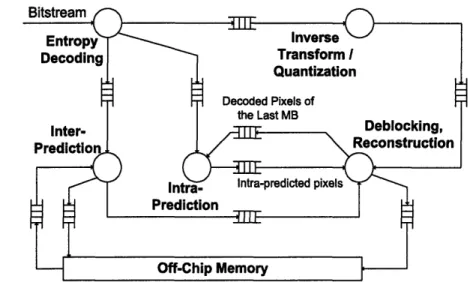
H.264 is widely being used for video compression and there is surging demand for efficient H.264 decoder hardware. Figure 3-1 shows a specification of H.264 decoder; each module has data-dependent latencies. The entropy decoder module and the inter-prediction module will be examined, which will show that an architecture which targets average case latency has a performance benefit over a conventional pipelined design that assumes the worst case.
Figure 3-1: High-level Module Description of H.264 Decoder
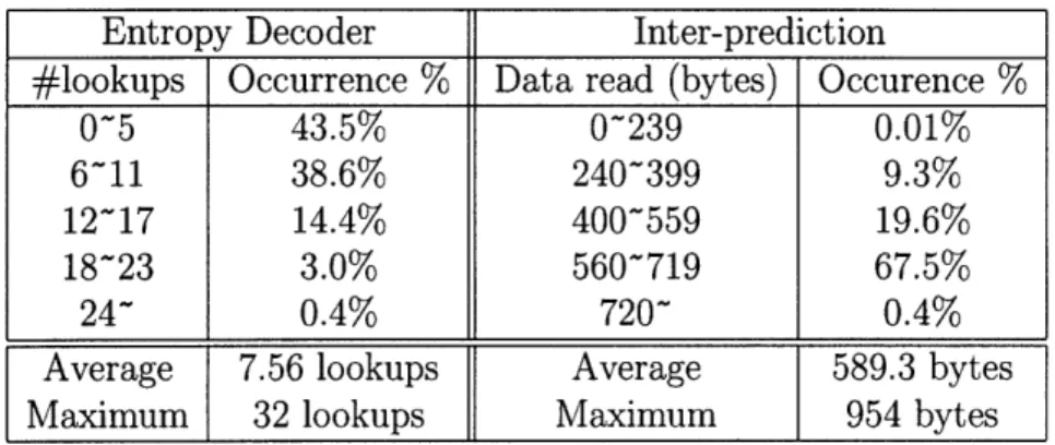
The entropy decoder module in H.264 decoder performs context-adaptive variable length decoding (CAVLD) that uses 20 different code tables. Each image block from the input stream requires access to different code tables and the number of table lookups varies significantly across inputs. Because the table lookup and following computations take up the majority of time in entropy decoding, one can assume that the latency of the entropy decoder module is proportional to the number of table lookups for each input (image block). In the inter-prediction module, the latency is dominated by the number of pixels it reads from reference frames, which depends on the input block's offset from the reference block (motion vector). Therefore, the latency of inter-prediction module is again highly dependent on the input block and can be different for each input.
Table 3.1 shows the profiling results of both modules for a standard input stream 'toys and calendar', illustrating the large difference between the worst-case latency and the average-case latency.
Table 3.1: Profiling Results of H.264 Decoder Modules for a Standard Input
If each module is completely decoupled through infinite size FIFOs, the average-case design on a diastolic array will have 40% to 80% lower latency (or higher through-put) compared to the pipelined design that always performs the maximum number of operations, i.e., performs 32 lookups in the entropy decoder and reads the entire reference frame in the inter-predicton module.
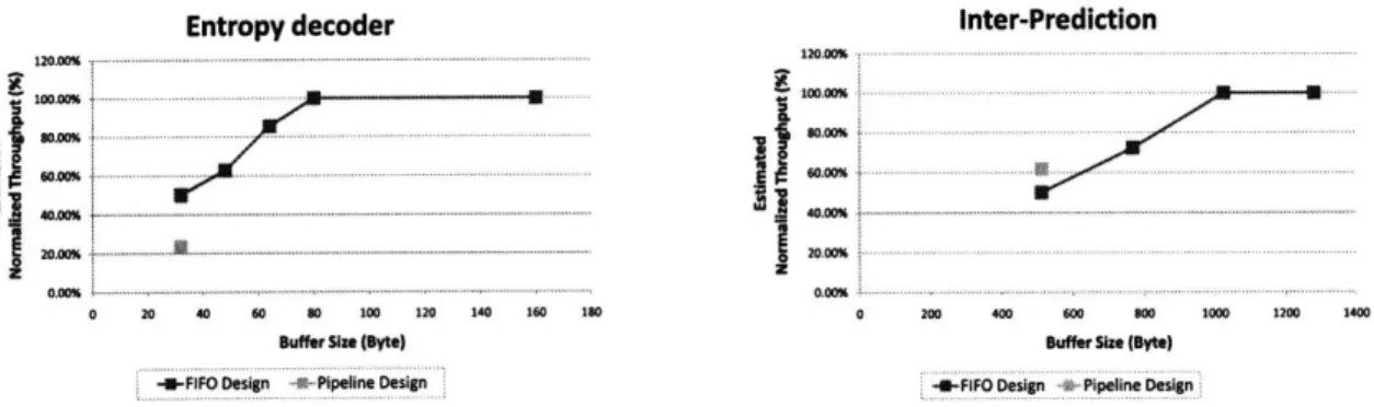
In practice, however, the throughput could be lower than the average case if the FIFO is not large enough because individual module latencies vary from input to input. The simulation results of the throughput of each H.264 module as a function of a FIFO buffer size are shown in Figure 3-2. The simulation assumed that all of other modules have a fixed throughput that is the same as the target module's average. The figure also shows the estimated throughput for a conventional pipelined design where the maximum number of operations are performed regardless of the input.
From the results, the performance of the single-entry FIFO design is seen to be worse than the pipeline design for inter-prediction, and better for entropy decoder. In the inter-prediction module, this is because a producer in the single-entry FIFO design in this simulation stalls until a consumer finishes using it, thus serializing the producer and the consumer. On the other hand, in the pipeline design of the
inter-Entropy Decoder Inter-prediction
#lookups Occurrence % Data read (bytes) Occurence %
0-5 43.5% 0~239 0.01%
6~11 38.6% 240~399 9.3%
12~17 14.4% 400-559 19.6%
18~23 3.0% 560~719 67.5%
24~ 0.4% 720~ 0.4%
Average 7.56 lookups Average 589.3 bytes Maximum 32 lookups Maximum 954 bytes
prediction module, a producer is assumed to be able to write into pipeline registers at the same cycle when a consumer is reading the register value produced in the previous cycle. As a result, the total latency of the single-entry FIFO design could be worse than the pipeline design if the sum of average latencies of the producer and the con-sumer is larger than the worst-case latency of the producer and the concon-sumer. From Table 3.1, the average amount of data read in inter-prediction is greater than half of the maximum amount. Therefore, the sum of average latencies of the producer and the consumer becomes larger than the worst-case latency, and hence the performance of the single-entry FIFO design is worse than the pipeline design. However, in the entropy decoder module, the average number of lookups in entropy decoder is only about 24% of the worst case, and therefore the performance of the single-entry FIFO design is better than the pipeline design.
Note that if FIFOs have more than one entry for data, there are no such serial-ization effects and the results clearly illustrate the benefit of the average-case design over the pipelined design. The figure also shows that the throughput increases as buffer size grows before saturating, which demonstrates that it is important to have a large enough FIFO in order to achieve the best possible throughput.
Entropy decoder Inter-Prediction
MooM ..--.---.- . .ooo.-120.0m. . ... ...
.... . . .- ... . -. . . . O %
...
0
Mi....
...
...
j2...00%.
0 20 40 60 80 100 120 140 160 180 0 200 400 00 00 1000 1200 1400
Buffer Sine (yte) Buffer Size (Byte)
-- FIFO Design -Pipeline Design - FIFODesign -Pipeline Design
Figure 3-2: FIFO size vs. Data Throughput of H.264 Decoder Modules: Entropy Decoder and Inter-prediction
From these experiments, it is clear that the average-case design can have sub-stantial performance benefit over a worst-case design. Unfortunately, implementing FIFOs on conventional reconfigurable substrates such as FPGAs is very expensive due to the routing overhead connecting FIFO buffers and logic, which results in
sig-nificant performance loss in each module. As a diastolic array has dedicated hardware to support FIFO-based communication between computing elements, designers can efficiently exploit the benefit of average-case design.
3.3
Example: Performance Modeling
Performance modeling estimates the performance of a hardware design so that archi-tects can evaluate various alternatives at an early stage of the design. Fast perfor-mance modeling is important because it enables a designer to explore more design choices for more complex designs. Traditionally, performance modeling has been done purely in software. However, to further speed up performance modeling, recent work such as HAsim [32, 31] and FAST [7] use FPGAs to implement performance modeling in hardware.
The goal of performance modeling is simply to obtain timing information of a target system, not to faithfully emulate the target system cycle by cycle. Therefore, a performance model may take multiple substrate clocks (FPGA or array processor clocks) to perform a single-cycle operation on the target machine. For example, an associative cache look-up can be implemented with a single-ported SRAM in multiple cycles by checking one cache line in each cycle as long as the model counts one model cycle for all these look-ups. The latency of such a cache module varies dramatically depending on the input: one cycle if there is a hit in the first line that is checked or many cycles to check every line in the set in the case where an access eventually incurs a cache miss. Therefore, the performance modeling application has significant differences between the average-case latency and the worst-case latency.
In the same way that a diastolic array improves H.264 performance, it can also improve the performance of the performance modeling application by only performing necessary operations with an average-case design. The architecture will be able to achieve much greater performance than FPGAs thanks to the FIFO support for the average-case design and its word-level granularity.
3.4
Other Applications
Another interesting application for diastolic arrays is processor emulation. Unlike per-formance modeling, processor emulation faithfully simulates all cycle-by-cycle hard-ware operations of target systems. Even though processor emulation needs to perform all operations in the design, each module in a processor will have a different number of operations to perform depending on the input. As a result, average-case design can still be greatly beneficial.
H.264 encoder is also a very interesting application for diastolic arrays as it has more modules and more complex data flow than H.264 decoder. Many DSP appli-cations such as IEEE 802.11a/11g wireless LAN transmitter (cf. Section 5) are also well-suited to the architecture for similar reasons. In general, if an application can be modularized to a number of modules and the latency of each module significantly varies depending on input and the average latency is much less than the worst-case la-tency then a diastolic array can provide performance benefits over traditional systolic arrays or pipelines.
Chapter 4
Diastolic Architecture
This chapter describes a candidate diastolic array architecture. The architecture provides guarantees of bandwidth and buffer space for all data transfers through:
* Non-blocking, weighted round-robin transfers of packets corresponding to dif-ferent virtual FIFOs (VFIFOs) from one physical FIFO (PFIFO) to a neighbor, * Ratioed transfer of packets corresponding to the same VFIFO from a PFIFO to its neighbors and in-order reception of said packets at PFIFOs to enable composite-path data transfers where sub-paths split and reconverge (cf. Figure 4-1(b)), and
* Allocation of PFIFO space to particular VFIFO packets to avoid deadlock and to maximize throughput.
Section 4.1 depicts the overall architecture of diastolic arrays. The processing element and the interface between processing elements and PFIFO are described in Section 4.2, and Section 4.3 shows how PFIFOs work and communicate with other PFIFOs.
Additionally, Section 4.4 describes optional hardware support for data synchro-nization through FIFO connections, using a notion of system time. It should be noted that system time is only for performance optimization and not essential for through-put guarantee and deadlock avoidance. Section 4.5 briefly introduces the diastolic architecture simulator.
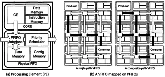
A single-path VFIFO A composite-path VFIFO (a) Processing Element (PE) (b) A VFIFO mapped on PFIFOs
Figure 4-1: A PE Architecture and a Single-path and a Composite-path Route of a VFIFO
4.1
Microarchitecture Overview
A diastolic array realizes the high-level computation model with a grid of processing elements (PEs) each with an attached PFIFO as shown in Figure 4-1 (a). In this archi-tecture, all PEs operate synchronously using a single global substrate clock. PFIFOs are connected to neighboring PFIFOs and support many VFIFOs with synchroniza-tion mechanisms; from the PE's perspective, PFIFOs appear as many VFIFOs. In our candidate architecture, PEs are simple MIPS-like processors and the PFIFO net-work consists of 4 nearest-neighbor connections. In this architecture, each PFIFO can take up to 5 inputs (4 neighbors and the PE) and produce up to 5 outputs in each clock cycle. PFIFOs in the periphery of the PE grid interface with I/O pads in one direction. I/O logic will attach VFIFO ID's to packets if they are not given by the external source so they can be routed to the appropriate destination.
Figure 4-1 (b) illustrates how a VFIFO is implemented with multiple PFIFOs - a single-path and a composite-path VFIFO marked by black arrows. In both examples, the VFIFO connects the top-left PE (producer) and the bottom-right PE (consumer). PFIFOs need to route VFIFO packets along single- as well as composite-path routes (cf. Section 4.3). The synthesis tool statically determines the routing and maps each
VFIFO to corresponding PFIFOs along possibly multiple paths where each individual path has a pre-determined rate or flow (cf. Section 5.7).
4.2
PE and PE-to-PFIFO Interface
Our initial PE design is based on a MIPS-like 32-bit 5-stage in-order processing core. The ISA for computation is almost identical to the MIPS ISA with a branch delay slot allowing the use of a standard MIPS compiler backend to generate efficient PE code. We use the gcc backend for MIPS in our synthesis framework. The main difference between the PE and a traditional MIPS core is in its support for VFIFO mechanisms; our PE supports additional instructions for VFIFO communication. Table 4.1 summarizes the additional PE instructions.
Instruction Operands Descriptions
deq Rt, Rs Dequeue data from VFIFO $Rs and write to Rt (blocking) deqi Rt, imm Dequeue data from VFIFO imm and write to Rt (blocking)
enq Rt, Rs Enqueue $Rt to VFIFO $Rs (blocking)
enqi Rt, imm Enqueue $Rt to VFIFO imm (blocking)
drdy Rt, Rs $Rt+-1 if data is ready from VFIFO $Rs, 0 otherwise drdyi Rt, imm $Rt<-1 if data is ready from VFIFO imm, 0 otherwise erdy Rt, Rs $Rt+-1 if VFIFO $Rs can accept data, 0 otherwise erdyi Rt, imm $Rt<--1 if VFIFO imm can accept data, 0 otherwise Table 4.1: Basic Instructions for VFIFO Communication
In each cycle, a PE can dequeue a 32-bit value from a VFIFO, by using a blocking instruction deq and deqi specifying a VFIFO number and a destination register. If data of the VFIFO is ready in the attached PFIFO, this instruction dequeues data from the VFIFO and updates the destination register. Otherwise, the instruction will stall the processor until data becomes ready.
Before issuing blocking dequeue instructions, the PE may first check the status of the VFIFO by drdy or drdyi instructions and use branch instructions to use dequeue instructions only if data is ready. This explicit check allows the PE to continue its computation instead of just waiting when no data is ready for a VFIFO.
enqueue instruction enq and enqi specifying a data value and a VFIFO number. This instruction enqueues the value (in a register) into the VFIFO if the attached PFIFO has an available entry for that VFIFO. Otherwise, the instruction stalls the PE until the VFIFO becomes available.
The PE can also use erdy or erdyi instructions to check the availability of target VFIFO before using blocking enqueue instructions. When the PFIFO attached to the PE says that it can accept data for the specified VFIFO, it reserves buffer space for the VFIFO because data of other VFIFOs may fill empty buffer space before the PE actually sends data to be enqueued.
4.3
Physical FIFOs (PFIFOs)
PFIFOs implement the VFIFOs and synchronization mechanisms through backpres-sure and idling. In addition to the PE-to-PFIFO interface described in Section 4.2, a PFIFO has to fulfill two main goals:
* Allocate buffer space for VFIFO packets that cannot be used by other VFIFOs to guarantee deadlock avoidance and maximum transfer rate.
* Route packets corresponding to each VFIFO with appropriate rates. The routes may be single- or composite-path routes, with the latter requiring increased PFIFO complexity. When transferring data for a VFIFO, a PFIFO must ensure that the receiving PFIFO has space available for the corresponding VFIFO. PFIFOs perform the following four steps in order to achieve these goals.
4.3.1
Buffer Allocation for Virtual FIFOs
Each PFIFO has one data memory that is shared among all VFIFOs mapped to the PFIFO. The synthesis tool statically partitions a large part of this data memory amongst VFIFOs by setting the pointers in the configuration table. Each VFIFO assigned to a PFIFO has a partition size of at least one packet and these partitions are exclusively used for each VFIFO while the remaining data memory can be shared
by all of the VFIFOs. In this way, the synthesis tool can guarantee that each virtual FIFO has the necessary number of FIFO entries to avoid deadlock no matter what the traffic pattern is. Further, when hardware resources allow, the synthesis tool allocates buffer space to achieve the maximum transfer rate for each VFIFO across the corresponding PFIFOs. The synthesis tool determines the buffer allocation for deadlock avoidance and maximum transfer rate with information given by application specification and profiling results (cf. Section 5.8).
4.3.2
Scheduling for Composite-path Routes
In each substrate cycle, all PFIFOs try to send out packets to their next hops. Ob-viously, PFIFOs need to know to which PFIFO packets for each VFIFO should be sent. The configuration table in each PFIFO stores information about each VFIFO that maps to this PFIFO as given by the synthesis tool, and each entry of the table contains the VFIFO ID, and a list of possible previous and next PFIFOs. When a VFIFO has a single-path route or a PFIFO is not a split point of the VFIFO, there is only one possible next PFIFO specified in the configuration table.
However, if a PFIFO corresponds to a split point for a composite-path VFIFO route, then the PFIFO need to choose one from a number of possible next PFIFOs in each substrate cycle. The routing step during the synthesis computes the predefined ratios of the flow rates for the different directions, and the PFIFO sends out packets for the VFIFO in each direction in a deterministic order to control the flow rates. For example, if there are two possible next PFIFOs A and B at a split point and the routing specifies that A requires two times more bandwidth than B, then the PFIFO sends the first two packets for the VFIFO to A, and sends the next packet to B, repeatedly.
As packets are routed in deterministic order, they can be received in order at the reconvergent PFIFO. At a PFIFO that is a reconvergent point for a VFIFO, an acknowledgement algorithm allows an incoming packet from multiple neighbors to come in at appropriate ratios so as to guarantee in-order communication through
this PFIFO, and to ensure that deadlock due to out-of-order packets will not occur. 1 The ratios in the acknowledgement algorithms depend on the throughput ratios of the split and reconvergent flows and are determined after the routing step as described in Section 5.8. PFIFOs are then configured with appropriate weights for the round-robin send algorithm and ratios for the acknowledgement algorithms.
4.3.3
Arbitration of VFIFOs with the Same Destination
After the process described in Section 4.3.2, next hops for all packets in each PFIFO are known. As multiple VFIFOs may share the same channel to another PFIFO, a PFIFO may have many packets corresponding to different VFIFOs which are to be sent to the same destination for a given cycle. In this case, the PFIFO selects one VFIFO for each subsequent hop in a weighted round-robin fashion and forwards its data. This is done in a non-blocking fashion; if there is no data available for a VFIFO, the next VFIFO is selected. The algorithm does not wait for data to become available. The weights are determined after the routing step (cf. Section 5.7) to meet the desired flow rates and applied in the configuration step (cf. Section 5.8).
4.3.4
Data Reception Protocol
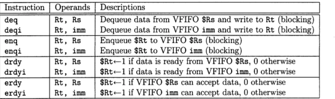
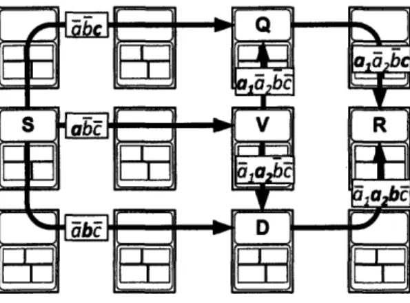
To ensure that the receiving PFIFO does have an entry available for the particular VFIFO, the PFIFO uses a two-phase protocol. In the first cycle, the PFIFO sends data with an associated VFIFO ID to the next hop. However, the PFIFO does not immediately remove the entry from its data memory. In the second cycle, the receiving PFIFO replies through a dedicated wire whether the data was accepted or not; the receiver rejects the data if there is no space remaining for this VFIFO's packet. The sending PFIFO removes data only after it receives a positive acknowledgement in the second cycle. This two-phase protocol is pipelined to allow a new data transfer every cycle, and is illustrated in Figure 4-2.
1A later packet should not use up space in a reconvergent PFIFO on a composite path and block
- l Data
> Control
PFIFO1 PFIFO2 PFIFO1 PFIFO2 PFIFO1 PFIFO2
vF END a
:DONE
EN i]]j[[Z.·oi I I IX
ZT
cycle = 0 1 cycle = 1 cycle = 2
PFIFO1 chooses VFIFO1 and sends a. PFIFO1 now chooses VFIFO2 and sends c. PFIFO1 chooses VFIFO1 again and sends b.
I PFIFO2 accepts a and sends DONE signal. I PFIFO2 Is full, so it sends FULL signal.
PFIFO1 removes a from its buffer. PFIFO1 will send c again in the next turn.
Figure 4-2: The PFIFO to PFIFO Interface
4.4
Performance Optimization: Timestamp
In addition to the basic diastolic architecture illustrated in the previous sections, the candidate architecture examined in this thesis has optional hardware support to
optimize performance for some types of applications using timestamping.
Conceptually, the system time in diastolic arrays is similar to clock cycles in synchronous circuits. In synchronous circuits, combinational logic takes updated inputs and produces new outputs in each clock cycle. In a diastolic array, in each system time slice, a processing module reads a set of input FIFOs and produces results for a set of output FIFOs. Note that one unit of system time may correspond to multiple clock cycles of a diastolic array chip (substrate cycles); a processing module can take multiple substrate cycles to produce outputs from inputs, and this number can vary depending on the input data.
In H.264 decoder application, for an instance, each module processes one mac-roblock 2 per one system "clock". As each module may take different number of substrate cycles for a system clock, modules need to be synchronized according to system time.
If the number of data produced and consumed at each system time is constant for all PEs, synchronization is automatically achieved through FIFO connections be-cause after consuming a fixed number of data packets a consumer will always proceed
2
A macroblock in H.264 is a small rectangular block of pixels which is the minimum unit of decoding process.
to the next system cycle. However, if any producer sends out different numbers of data packets depending on input, or any consumer takes different numbers of data packets, then there needs to be an explicit mechanism for system time synchroniza-tion. For example, the size of macroblock in H.264 decoder varies for each system time, depending on input video streams. Therefore, any consumer taking pixels of macroblocks does not know how many data packets it should take from its producer for a given system time unless there is auxiliary information or control telling it when to stop taking data.
One simple way to achieve synchronization without architectural support is to use "end" packets for each VFIFO, which indicate that there will be no other data for a given system time. This is done by software very simply, but one additional packet needs to be transferred to its consumer for every VFIFO, for every system time. Most other software schemes for the synchronization cost the diastolic array network bandwidth as well as PE computation time.
Timestamping provides hardware support for system time synchronization. It lets PFIFOs handle the synchronization instead of PEs so that the computation time of PEs and especially the PE-to-PFIFO communication time at the consumer side can be significantly saved. In this scheme, each PE individually tracks the current system time and attaches a time-stamp to each FIFO packet, which indicates when the receiving PE should use the packet. At the consumer side, a PE specifies its system time and the attached PFIFO determines whether arrived data can be consumed, or whether it needs to wait for incoming data, or whether there will be no data for the given system time. For this purpose, each VFIFO has its own counter for the system time (VFIFO time in the figure). If the VFIFO time is greater than its current time, it indicates to a consumer that the producer does not have more data for the current time and to a producer that the consumer does not need more data. This scheme increases communication bandwidth for timestamps. However, the information for synchronization is integrated in data packets so that PEs can be properly synchronized while only transferring necessary data through FIFOs.
pro-VFIFO time = 3
producer
consumer
deqRdy?
time = 3 time = 3
wait -data for time 3 may come later.
i) the consumer doesn't know whether data for time 3 will come.
VFIFOtime=3 c4
producer T 1FF consumer
time = 4 time =3
ii) the producer proceeds to time 4 and sends proceed signal to VFIFO.
VFIFO time =4
producer I consumer
deqRdy?
time = 4 time=3 1 4
none - confirm there is no data for time 3
iii) the termination of the producer allows the consumer to proceed.
a) Termination by producers VFIFO time = 7 producer
Fd?
e -- consumer deqRdy? time= 7 - time = 3 L J rdyi) data is ready for the consumer. VFIFO time = 7
producer +-- consumer
06
~proceed-time = 7 discard time = 4
ii) CASE 1 -the consumer proceeds with discard option.
VFIFO time = 7
producer *-- consumer
proceed-time = 7 hold time -= 4
ii) CASE 2 - the consumer proceeds with hold option.
b) Termination by consumers
Figure 4-3: Optimization through Explicit Synchronization by Timestamp
ducers and consumers without transferring data (see Figure 4-3). Both producers and consumers can explicitly notify a VFIFO to increment the VFIFO time. Additionally, a consumer can choose whether a FIFO should keep data for the past time slices. If the consumer indicates that it would not need old data then the FIFO will discard all data with an old time-stamp. The performance benefit due to explicit synchroniza-tion can be significant especially when the consumer decides not to take any data for a certain period of system time because a number of packets can be discarded in the PFIFO, without spending any substrate cycles of the PE. An example of this case is the ALU module in the processor emulator application: if the module resolves a branch and knows it should discard the following instructions, it just explicitly moves to the next valid system time and the PFIFO discards every invalid instruction.
4.5
Diastolic Architecture Simulator
The candidate diastolic architecture was simulated by a cycle-accurate software sim-ulator written in the C++ language. The simulation framework provides diastolic array components such as PFIFOs, PEs and I/Os, and a simulation file uses these
components to define an array network and fetch the configuration bits for a target application to each component. The PE components are connected to another simu-lator, which is a 5-stage pipelined MIPS simulator for this candidate architecture.
This simulator allows fast microarchitectural exploration of diastolic arrays by turning on or off some of the features described in this chapterm, such as composite-path routing or timestamping. This simulator can also perform the profiling steps in the synthesis flow by using ideal FIFO connections rather than PFIFO connections, as described in Section 5.3.
Chapter 5
Synthesis Flow
While we described a candidate diastolic architecture in Chapter 4, various PE mi-croarchitectures and PFIFO network topologies can be supported with the synthesis flow described in this chapter.
The challenge when targeting an architecture with nearest-neighbor communica-tion is efficiently mapping applicacommunica-tions that exhibit significant long-distance commu-nication. This problem is made tractable in diastolic arrays by statically allocating both bandwidth and buffer space for communication that can be shared by many logical channels, allowing us to focus on maximum average throughput, while largely ignoring communication latencies.
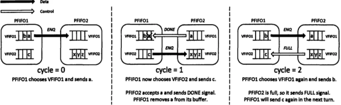
5.1
Synthesis Overview
The synthesis flow for diastolic arrays is illustrated in Figure 5-1. The input for synthesis is an application specification that is a high level description of the hardware design (cf. Section 5.2). Functional modules in the specification are grouped or partitioned by synthesis tools so each module corresponds to a PE of diastolic arrays (cf. Section 5.4). This generates PE descriptions and VFIFO specifications and PE descriptions are compiled to configuration bits for each PE (cf. Section 5.5). From VFIFO specifications, the PE placement step explores candidate placements which are used in VFIFO routing (cf. Section 5.6). After a feasible or the best route is
From Profiling II Highe"vel Profiling Result I ______________I Configuration
Figure 5-1: Synthesis Flow for Diastolic Arrays
found, PFIFO buffers are allocated to VFIFOs (cf. Section 5.7), and finally PFIFO configuration bits are generated according to the synthesis results (cf. Section 5.8).
Note that module grouping and partitioning, VFIFO routing, and buffer allocation step take additional input from different types of profiling results. The profiling is done by software simulation and provides information about the target application so the synthesis tool can optimize the performance. Section 5.3 will describe each profiling step.
Module Group & Partition
5.2
Application Specification
Synthesis begins from a specification of the hardware design as finite state machine (FSM) modules described in C that communicate via virtual FIFOs (VFIFOs). The specification will also provide minimum VFIFO sizes that ensure that the design does not deadlock. We will assume that for VFIFO i, zi packets are required, with pi bits in each packet. In most cases, zi is determined by the maximum number of packets that the VFIFO needs to hold in order to synchronize PEs. For example, if a producer sends out up to 3 packets per system time (cf. Section 4.4) and its consumer takes data from 5 system times ago, the VFIFO between them may need to hold 15 packets in order to synchronize them.
The application specification is simpler than synchronous data flow [25], and sim-ilar to an intermediate output of a parallelizing compiler such as StreamIt [35] after parallelism extraction, but could also be directly written by a designer. Minimum requirements for FIFO sizes can be determined by compilers such as StreamIt [15]. Modules in the specification may be grouped or partitioned during the synthesis flow. Therefore, modules in the specification does not have a one-to-one matching with PE hardware.
A high-level view of the specification of an H.264 decoder application was previ-ously shown in Figure 3-1. The goal of synthesis is to maximize average throughput, which requires that bandwidth and buffer space be properly allocated to all VFIFOs. The H.264 decoder example will be used to illustrate each synthesis step throughout this chapter.
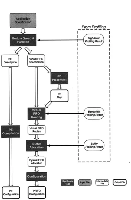
5.3
Profiling
Profiling can provide important information about the performance of target appli-cations which cannot be attained from their specifiappli-cations. There are three different profiling steps performed through the synthesis flow for diastolic arrays. Table 5.1 summarizes those profiling steps.
Profiling Step Computational Node VFIFO Connection I Purpose
High-level Profiling High-level module, isolated Ideal To group or partition modules
Bandwidth Profiling PE, correlated Ideal To determine demanded throughput
Buffer Profiling PE, correlated shared link PFIFOs To determine buffer requirement (individual buffer)
Table 5.1: Profiling for the Synthesis for Diastolic Arrays
5.3.1
High-level Profiling
High-level profiling takes the application specification described as communicating high-level modules and determines how much computation each module performs. This information is used for module grouping and partitioning so that after grouping and partitioning each PE has a similar amount of computation time. In high-level profiling, each high-level module is simulated separately on an array PE and a his-togram of module latency over different module inputs is produced, which gives a range of latency as well as an average. Module latencies are computed as processor cycles per packet produced - each module produces data packets that correspond to a VFIFO. This is converted into cycles per bit produced. The case study of en-tropy decoder and inter-prediction modules in Section 3.2 is an example of high-level profiling.
5.3.2
Bandwidth Profiling
Bandwidth profiling takes place after module grouping and partitioning. At this time all PEs and the entire network are simulated; consumers should wait until producers send out data so the throughput of each VFIFO in bandwidth profiling reflects pos-sible correlations between VFIFOs. However, the VFIFO connections are assumed to be ideal: each VFIFO has a very large buffer 1 and VFIFOs do not share physical links and have minimum latency. If there is a target system throughput, then the output of the system is pulled at this rate. 2 In this step, profiling computes a rate IThe buffer size is not infinite because a FIFO with infinite buffer size will decouple the rate before its producer and after its consumer when the producer is faster.
2For H.264 decoder, the target system throughput was set to decode HDTV video stream
distribution and average transfer rate di in bits per second for each VFIFO i, which is a key measure used in the routing step. These rates are correlated and depend on the target system throughput if specified. Because the VFIFO connections are ideal and the performance is unaffected by routing (either by latencies or by congestion), these rates become the optimal goal for the routing step.
5.3.3
Buffer Profiling
The last profiling step is buffer profiling which provides a distribution of buffer size and average buffer size mi in bits for each VFIFO i that is required for sustaining the average transfer rate di. This is derived from the variation in occupied buffer sizes during simulation.
The simulation for buffer profiling takes account of the PFIFO network; VFIFOs have various latencies and physical links between PFIFOs are shared by multiple VFIFOs. Unlike the actual diastolic architecture, however, VFIFOs do not share the memory of PFIFOs. Each VFIFO is assumed to have a large dedicated buffer. Therefore, the average buffer size measured during buffer profiling is not affected by other VFIFOs.
If a producer is always faster than its consumer in a given producer-consumer pair, then the buffer of the corresponding VFIFO always becomes full and mi has no actual bound. In this case, the minimum buffer size of the VFIFO that does not affect other rates is chosen.
5.4
Module Grouping and Partitioning
Based on the high-level profiling results, modules are grouped or partitioned. Group-ing involves assignGroup-ing two or more modules to the same PE, while partitionGroup-ing involves splitting a module across multiple PEs in order to exploit parallelism and reduce the effective average latency.
Module grouping is done if there are more modules than the number of available PEs, or if there is tight feedback between modules whose latency can affect
through-Figure 5-2: H.264 Specification after Module Group and Partition
put. 3 When two modules are run on the same PE, their latencies will increase to their sum. If the inverse of this combined latency is equal to or more than the VFIFO rates corresponding to each of these modules, the modules can be grouped together. Grouped modules are executed in interleaved fashion on a PE. If a module does not have inputs available it cedes to the next module. After a module execution, if there is no space available in the PE's FIFO for the result, the module will stall until space is available. 4
If it is impossible to obtain the target system throughput, the modules whose latencies are too high are targets for partitioning. Partitioning mostly depends on the parallelism that can be extracted from actions described in the specification. For example, if a module performs actions A, B, C and D, where B depends on A, and D depends on both C and A, we can execute actions A and B on a PE, and C and D on a different PE, possibly improving average latency, since C and A 3If a tight feedback connection cannot be removed by module grouping, the synthesis tool tries to minimize its latency (cf. Section 5.6 and Section 5.9).
4The actual latency becomes larger than the sum because of increased congestion in the VFIFOs
can be simultaneously executed. Note that partitioned modules introduce additional VFIFOs that communicate between PEs, and a partition has to be carefully selected to optimize the resulting average latency which depends on the additional FIFO latency. Modules are not partitioned if a large number of additional FIFOs are required. Automatic partitioning is a difficult problem that corresponds to parallelism extraction, and is not a focus of this thesis.
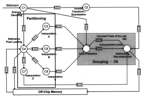
An example of a module grouping and partitioning result for the H.264 decoder is shown in Figure 5-2. The intra-prediction module and deblocking module were grouped together, and the inter-prediction module was partitioned across PEs. The high-level profiling results showed that the inter-prediction module needs a lot of com-putation time; the partitioning was done by extracting parallelism in the module, and the grouping was done to eliminate tight feedback. After grouping and partitioning, the profiling step is run again to determine the new module and VFIFO latencies.
5.5
PE Compilation
After the module grouping and partitioning step, the system has a set of PEs with corresponding modules. Modules are compiled to each PE in a decoupled way and the results of the compilation provide each PE with scheduling information and ex-ecutables. The PEs in the diastolic architecture have an ISA that is a subset of the MIPS ISA and modules are described in the C language. The gcc backend for the MIPS-II processor was used in the experiments of Chapter 6.
All communications to other PEs are through PFIFOs with FIFO control, which the compilation step is aware of only at the level of writing and reading data values to and from the VFIFO. A PE will wait on a given read (dequeue) instruction when there is no data available, or on a write (enqueue) instruction when the output FIFO is full. Therefore, the compilation step need not know about the routes and the timing of data communication of VFIFOs.