HAL Id: hal-01139768
https://hal.archives-ouvertes.fr/hal-01139768
Submitted on 7 Apr 2015
HAL is a multi-disciplinary open access
archive for the deposit and dissemination of
sci-entific research documents, whether they are
pub-lished or not. The documents may come from
teaching and research institutions in France or
abroad, or from public or private research centers.
L’archive ouverte pluridisciplinaire HAL, est
destinée au dépôt et à la diffusion de documents
scientifiques de niveau recherche, publiés ou non,
émanant des établissements d’enseignement et de
recherche français ou étrangers, des laboratoires
publics ou privés.
Distributed under a Creative Commons Attribution - NonCommercial - NoDerivatives| 4.0
International License
Influence of neodymium concentration on excitation and
emission properties of Nd doped gallium oxide
nanocrystalline films
A Podhorodecki, M Banski, J Misiewicz, Céline Lecerf, P Marie, J. Cardin, X
Portier
To cite this version:
A Podhorodecki, M Banski, J Misiewicz, Céline Lecerf, P Marie, et al.. Influence of neodymium
concen-tration on excitation and emission properties of Nd doped gallium oxide nanocrystalline films. Journal
of Applied Physics, American Institute of Physics, 2010, 108 (6), pp.063535 1-6. �10.1063/1.3484039�.
�hal-01139768�
Influence of neodymium concentration on excitation and emission properties of Nd
doped gallium oxide nanocrystalline films
A. Podhorodecki, M. Banski, J. Misiewicz, C. Lecerf, P. Marie, J. Cardin, and X. Portier
Citation: Journal of Applied Physics 108, 063535 (2010); doi: 10.1063/1.3484039
View online: http://dx.doi.org/10.1063/1.3484039
View Table of Contents: http://scitation.aip.org/content/aip/journal/jap/108/6?ver=pdfcov Published by the AIP Publishing
Articles you may be interested in
Investigation on the compensation effect of residual carbon impurities in low temperature grown Mg doped GaN films
J. Appl. Phys. 115, 163704 (2014); 10.1063/1.4873957
Elevated temperature dependent transport properties of phosphorus and arsenic doped zinc oxide thin films J. Appl. Phys. 114, 223709 (2013); 10.1063/1.4845855
Improvement of (004) texturing by slow growth of Nd doped TiO2 films J. Appl. Phys. 112, 113505 (2012); 10.1063/1.4767361
Visible light emission and energy transfer processes in Sm-doped nitride films J. Appl. Phys. 111, 123105 (2012); 10.1063/1.4729911
Arsenic doped p -type zinc oxide films grown by radio frequency magnetron sputtering J. Appl. Phys. 106, 073709 (2009); 10.1063/1.3236578
Influence of neodymium concentration on excitation and emission
properties of Nd doped gallium oxide nanocrystalline films
A. Podhorodecki,1,a兲 M. Banski,1J. Misiewicz,1C. Lecerf,2P. Marie,2J. Cardin,2and X. Portier2
1
Institute of Physics, Wroclaw University of Technology, Wybrzeze Wyspianskiego 27, 50-370 Wroclaw, Poland
2CIMAP, CEA/UMR CNRS 6252/ENSICAEN, Université de Caen Basse Normandie, 6 Boulevard Maréchal
Juin, 14050 Caen, France
共Received 2 July 2010; accepted 29 July 2010; published online 24 September 2010兲
Gallium oxide and more particularly-Ga2O3matrix is an excellent material for new generation of
devices electrically or optically driven as it is known as the widest band gap transparent conductive oxide. In this paper, the optical properties of neodymium doped gallium oxide films grown by magnetron sputtering have been analyzed. The influence of the Nd ions concentration on the excitation/emission mechanisms of Nd ions and the role of gallium oxide matrix have been investigated. The grain size reduction into gallium oxide films have been observed when concentration of Nd increases. It has been found for all samples that the charge transfer is the main excitation mechanism for Nd ions where defect states play an important role as intermediate states. As a consequence Nd emission efficiency increases with temperature giving rise to most intensive emission at 1087 nm at room temperature. © 2010 American Institute of Physics.
关doi:10.1063/1.3484039兴
I. INTRODUCTION
Light emitting diodes or laser sources working in the near infrared region are under extensive investigation due to a wide range of their potential applications. Among many different solutions like quantum wells,1quantum dashes,2or quantum dots,3 and doping or codoping of semiconductors by rare earth 共RE兲, i.e., Nd, Er ions4,5 gives many new op-portunities for infrared light sources. Their exceptional prop-erties arise from the fact that their optical transitions take place among internal 4f orbitals, which are shielded from the environment by 5d-orbital electrons. It results in an emission with a narrow band and extremely stable wavelength, regard-less in some extent of the external conditions in matrix trans-parent in the wide spectral range. In addition, this concept gives many other new possibilities since this kind of matrices can be easily codoped by other ions covering a spectral range from 400–2000 nm.6
However, the main limitation of RE ions is their small absorption cross section due to electric dipole transitions which are forbidden according to Laporte’s rule. In addition, their low solubility in the matrix is reflected as ions cluster-ing which quenches their emission above critical, often very low共less then 0.1%兲, RE content. Thus, in order to increase their emission efficiency, crucial for practical applications, their excitation should be sensitized by an additional donor center, i.e., matrix,7 defects states,8 nanocrystals,4 or other molecules, i.e., molecular oxygen.9At these limited condi-tions for using RE ions as emitters in real devices, a better understanding of the excitation and quenching mechanisms should be investigated in details to optimize their optical properties.
The other important issue, to overcome for this kind of “discrete” light emitters is the poor electrical properties of matrices used as a RE ions host. Thus, even if optical pump-ing of RE ions via the energy transfer gives promispump-ing re-sults, electrical pumping became very difficult to realize in practice.
In the following, gallium oxide films were used as a host matrix of Nd3+ions. This material is well known as a
trans-parent conductive oxide with the widest band gap共4.9 eV兲, which can exhibit n-type semiconductor properties in case of some oxygen deficiency.10Thus, this material is a promising matrix for next generation optoelectronic devices working in a longer wavelength. Due to its low maximum phonon en-ergy 共⬃793 cm−1兲 共Ref.11兲 as compared to silicate glasses
共⬃1100 cm−1兲, and its high refractive index 共n=1.96 at
1.06 m兲 共Ref. 12兲 it is expected to provide significantly
high radiative decay rates and low nonradiative relaxation rates of RE excited-state levels. RE-doped gallium oxide is also a promising material for electroluminescent based devices.13–16Additionally, this matrix can exhibit good elec-trical properties when doped within.17
In the present work, gallium oxide films doped with vari-ous Nd3+concentrations have been investigated to determine their excitation mechanism and its evolution versus Nd con-tent in the matrix. The absorption, photoluminescence 共PL兲 and photoluminescence excitation 共PLE兲 measurements in the wide temperature range of 10–300 K have been per-formed for all the samples.
II. EXPERIMENTAL DETAILS
The neodymium doped gallium oxide films have been elaborated by magnetron sputtering of a Ga2O3 target
共99.99% purity兲 partially covered by Nd2O3共99.99% purity兲 a兲Electronic mail: artur.p.podhorodecki@pwr.wroc.pl.
JOURNAL OF APPLIED PHYSICS 108, 063535共2010兲
0021-8979/2010/108共6兲/063535/6/$30.00 108, 063535-1 © 2010 American Institute of Physics
pellets of calibrated shapes. Nd3+ concentration varies with
the r parameter, corresponding to the Nd2O3
pellets-to-Ga2O3 target surface ratio. The samples
investi-gated in our study had r in the range 0%–38.8%. The layers were grown on p doped and 共100兲-oriented Si substrates. During all the growth process, the 100 ° C temperature was kept constant. Post annealing treatments were carried out at 1000 ° C during 1 h under a continuous flow of nitrogen. A more detailed description of the sample preparation was al-ready presented in a previous article.18
Rutherford backscattering spectroscopy 共RBS兲 experi-ments were performed using a 4He+ ion beam with a 2.5 MeV Van de Graaff accelerator of the “Institut des Nano-sciences de Paris.”
Transmission electron microscope 共TEM兲 observations of the films were carried out using a JEOL 2010F TEM operated at 200 kV. Dark field images and high resolution TEM images were taken along the 关110兴 direction of the Si substrate. This direction allows a cross sectional view of the samples with the beam parallel to the film/substrate interface. Regarding the optical properties of the films, for PLE spectroscopy, samples were excited by a xenon lamp 共450 W兲 coupled with a monochromator 共Jobin Yvon TRIAX 180兲 and for absorbance measurements, a tungsten–deuterium halogen lamp was used. The visible PL, absorbance, and PLE signals were collected and transmitted by an optical fiber to the spectrometer 共HR4000 Ocean Optics兲 and di-vided by the light source characteristic. The PL spectra in the infrared spectral range were obtained by cooled linear In-GaAs array detector of 512 pixels coupled to the monochro-mator共Jobin Yvon TRIAX 550兲.
III. RESULTS AND DISCUSSION
The relationship between r values and Nd contents in the films has been established thanks to RBS measurements from as-deposited films, in which the Nd distribution is sup-posed to be homogeneous. Obtained in this way values are equal to 0.08 at. %, 0.94 at. %, 1.56 at. %, and 1.79 at. % of Nd for r = 24.2, 29.1, 33.9 and 38.8, respectively. Also, sec-ondary ion mass spectroscopy experiments are in progress and complementary results will be published in a forthcom-ing publication.19
As it has been already shown in previous works,20 all as-grown films are amorphous. Upon annealing treatment at 1000 ° C, the films become mostly crystalline. TEM images of cross-section views of annealed gallium oxide films are shown in Fig. 1. Figures1共a兲and1共c兲correspond to a film grown with r = 9.7%, which is equivalent to a Nd3+ atomic
concentration lower than 0.08%. The images show a rather good crystallinity of the film with a columnar growth more particularly in the upper part of the film 关Fig. 1共c兲兴. In the bottom part of the film关Fig.1共a兲兴, relatively large grains are visible with no texture or columnar structure. The average grain size is approximately 55 nm, but the size distribution is large共from 10 up to 100 nm兲. It is worth noting that voids 共brightest regions in the image兲 are also present in the film as well as amorphous regions 共gray regions兲. Figure 1共b兲 pre-sents a bright field TEM image of a sample prepared with
1.79% of Nd ions. A dark field image of this sample is also reported in Fig. 1共d兲. In this case, the average grain size is about 10 nm and then much smaller than the previous case. It is also interesting to notice that the grain size is more uni-form.
In our previous article,20 x-ray diffraction experiments demonstrated the formation of the stable-Ga2O3phase for
all r values upon annealing. This result was confirmed by high resolution TEM共HREM兲 observations of well oriented grains whose patterns were consistent with the above men-tioned structure. However, RBS experiments have revealed that, for low r values, the expected gallium oxide stoichiom-etry 共Ga2O3兲 is not reached and this was observed for both as-deposited and annealed films. Indeed, the stoichiometry evolves from Ga2O2.7 for low r values and tends to the
ex-pected Ga2O3 alloy for higher r values.
These results mean that, despite the formation of the
-Ga2O3phase in all cases, a more pronounced oxygen
de-ficiency is observed for low r values. Furthermore, a high degree of Nd doping favors the formation of-Ga2O3 nano-particles.
Regarding Nd localization in the film, local energy dis-persive x-ray diffraction 共EDX兲 experiments have been tempted for both samples of Fig. 1. No variation in the Nd concentration has been noticed for the lowest r value共9.7%兲. A more particular attention has been paid to grain boundaries but the Nd concentration remained lower than the detection limit of the spectrometer. Concerning the highest r value, significant Nd concentrations共up to 7%兲 have been noticed around the -Ga2O3 nanoparticles confirming a nonuniform distribution of the RE in the film and a pronounced presence of Nd in the surrounding of the -Ga2O3 nanoparticles. By
contrast, local composition measurements in the grains lead to a Nd concentration varying from 1.5 up to 2%.
FIG. 1. Bright field TEM images of annealed samples elaborated with共a兲 r = 9.7% and共b兲 r=38.8%. Dark field TEM images of the corresponding r values共c兲 and 共d兲, respectively. In the first case, columnar growth and rela-tively large grains are observed whereas in the latter case, a random growth prevails with a concomitant nanostructuration of the film.
063535-2 Podhorodecki et al. J. Appl. Phys. 108, 063535共2010兲
Figure2shows the PL spectra obtained for gallium ox-ide films with different Nd contents at two different excita-tion wavelengths, resonantly through the Nd3+ levels 共4I
9/2
→4
F5/2兲 at 787 nm 共thick red line兲 and nonresonantly at 266 nm共thin blue line兲. As we can see, for all samples excited by the UV light, a strong and complex green emission 共GE兲 band centered at 500 nm is clearly observed with subbands at ⬃440, 500, 550, and 600 nm 关see Fig. 2共b兲兴. This band is also present for undoped annealed sample. Moreover, emis-sion band covering a very similar energy range appears also for undoped but also not annealed sample 关Fig.2共a兲兴. How-ever, its intensity is much lower than for the annealed one 共factor ⬃40兲. Based on our observations, where the emission intensity for this GE band strongly increases with the anneal-ing, the energy levels responsible for this emission could be related to Ga2O3 nanoclusters共Ga2O3-nc兲, whose formation
is strongly enhanced by the annealing. These levels can be related to cluster’s core but more probable to energy levels 共defects or surface states兲 related to nanoclusters boundaries formation.
The blue side of observed emission bands in Ga2O3 can
be explained as originating from Ga vacancies共VGa兲, O
va-cancies 共VO兲,21 and Ga–O vacancy pairs in Ga2O3.22 In -Ga2O3, the donors共VO兲 were found to be gathered in
clus-ters that form a donor band 40 meV below the conduction band where gallium–oxygen vacancy pair clusters form an acceptor band 420 meV above the valence band. These levels are responsible for the formation of an exciton bound as donor-acceptor pair giving rise to a blue-GE band. In addi-tion, red band centered at about 706 nm has been already observed in-Ga2O3originating from the recombination of
an electron trapped by 共VO兲 donor and a hole trapped by
acceptor due to the nitrogen doping, presumably replacing oxygen in the lattice.23,24
Additionally, it has been found that the emission inten-sity of the GE band depends on the Nd content what can be seen in more details in Fig.3. This feature could be a con-sequence of more efficient coupling between the Ga2O3-nc
and Nd ions when the Nd content increases. In consequence, the averaged intensity of the Ga2O3-nc is reduced since part
of absorbed carriers is lost for Nd excitation. Unfortunately, when the Nd content increases, the shape of the emission band also changes and well resolved interference patterns are observed 关see Fig. 2共c兲for instance兴. Despite this thickness effect, a more detailed analysis of the effect of Nd doping on the visible emission intensities has been tempted and the integrated PL intensities have been extracted and shown in Fig.3. This figure will be discussed in the next paragraphs. Moving to Nd related emission, at this nonresonant ex-citation 共266 nm兲 emission appears only for samples with r values higher than 17.4%. Three main emission bands related to Nd ions have been observed for these samples centered at 900 nm, 1087 nm, and 1362 nm and related to transitions from 4F3/2 to 4I9/2, 4I11/2, 4I15/2 energy levels of Nd3+ ions, respectively, while the most intense band is at 1087 nm, which band is the most interesting from the application point of view. Above this concentration, Nd related emission strongly increases and the shape of Nd emission lines be-comes narrower and characterized by a Stark effect leading to at least two sets of emission lines at characteristic energies S1= 1.1462 eV共1081 nm兲 and S2= 1.1419 eV 共1085 nm兲.
On the other hand, when the samples are excited reso-nantly, unwanted emission band centered at 1100 nm can be observed for all Nd concentrations which band overlaps with the emission from Nd ions. We associated this band to a recombination process from the silicon substrate.25 Second, as for nonresonant excitation, emission from Nd ions appears clearly when r is above 17.4% and also characterized by the evolution of the emission line shape.
When comparing both PL spectra related to the emission from the Nd ions obtained at resonant and nonresonant exci-tations, two phenomena are observed with the increase in Nd content. First, in both cases, the Stark splitted lines become stronger and the peaks are well separated with a spectral narrowing. This implies that with the r increase, Nd sites distribution goes from a broad one共amorphous environment兲
FIG. 2.共Color online兲 PL spectra obtained for Nd doped gallium oxide films at two different excitation wavelengths: 266 共blue line兲 and 787 nm 共red line兲. All films have been annealed, excluded the one related to the 共a兲 spectra.共Scales have been adapted for better view兲.
FIG. 3. 共Color online兲 PL intensities for Nd ions and VIS emission vs surface ratio共r兲.
063535-3 Podhorodecki et al. J. Appl. Phys. 108, 063535共2010兲
to a sharper one共crystalline environment兲. Second, we deal with different contributions of the Stark splitted lines grouped at two different spectral positions, which is clearly observed for the highest r value. These results suggest that there are two main sites of Nd ions, where the ions at site-S2 are mostly excited during a nonresonant process.
Based on these observations, we can conclude that when the gallium oxide matrix is excited resonantly共787 nm兲, Nd ions placed at two averaged sites 共S1 and S2兲 are excited equally but when the matrix is excited nonresonantly 共266 nm兲 most of the ions which are excited are Nd ions “coupled to element” responsible for their high energy sensitization, i.e., energy levels related to Ga2O3-nc. Moreover, the
im-provement in emission line shapes is in agreement with our structural data which indicates that with Nd content the sto-ichiometry of the matrix became improved thus ions are placed in more crystalline environment.
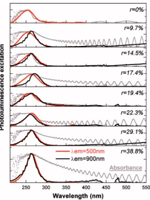
First of all, to confirm this coupling between the sensi-tizing element and the Nd ions, the integrated emission in-tensity has been calculated for both emission bands. An evi-dent correlation for these two emission bands共⬃500 and 900 nm兲 can be observed indicating that we deal with the “medium-coupling regime” since the element sensitizing the Nd ions is also responsible for the emission observed at 500 nm and only a part of excited carriers sensitizes the Nd ions. In the second step, to define the “sensitizing element” and to confirm the excitation energy transfer from it to the Nd ions, the excitation spectra have been measured for Nd emissions at 900 and 500 nm. Figure4shows the excitation and the absorbance spectra obtained from the reflectance data corrected by the Si substrate reflectance. As it can be seen for
each sample, the excitation spectra overlap each other and their maxima agree with the maxima of the absorbance bands centered at 250 nm 共4.95 eV兲. These observations indicate that the excitation mechanism responsible for the emission band at 500 nm is the same as for the emission at 900 nm.
In addition, it can be seen that the excitation band posi-tion, within the experimental errors, is approximately the same for all samples. Moreover, from the absorbance spectra, evident interference patterns are clearly resolved, confirming also our previous conclusions related to the origin of multi-peaks structure of the emission band centered at 500 nm. The obtained excitation 共absorption兲 band position is in good agreement with the values reported by other authors for the band gap of Ga2O3in phase. This indicates that the main
excitation mechanism of Nd ions is through the Ga2O3
ma-trix which plays the role of a sensitizer for the Nd ions. Since we know that the Ga2O3-matrix plays a crucial role in the
excitation of the Nd ions, the question is to know what kind of physical process is responsible for the excitation energy transfer after the carriers are absorbed by the matrix. Is this a direct excitation energy transfer from the grains to the lan-thanide ions4 or is this a defect mediated process?8 For the latter one, two main processes can be responsible for the energy transfer mediated by the defect states, namely nonra-diative dipole-dipole energy transfer 共Förster–Dexter兲 共Ref.
26兲 or charge 共electron/hole兲 transfer from donor/acceptor
states to Nd ions.9
To verify these hypotheses, the emission intensities for both emission bands at 500 and 900 nm have been recorded at different temperatures and at nonresonant excitation共266 nm兲. Results are shown in Fig.5. The PL integrated intensity of the visible emission band关Fig.5共a兲兴 obtained for undoped
FIG. 4. 共Color online兲 PLE spectra obtained both for emission at 500 nm 共red line兲 and emission related to Nd ions at 900 nm 共dark line兲 for samples containing different amount of Nd ions. Additionally, absorbance spectra have been given共dotted line兲.
FIG. 5. 共Color online兲 Normalized at 10K integrated PL intensities of the 500 nm共a兲 and 900 nm 共b兲 bands, measured at different temperatures and obtained for samples with different Nd contents at 266 nm excitation wavelength.
063535-4 Podhorodecki et al. J. Appl. Phys. 108, 063535共2010兲
and doped with r = 19.4% samples decreases with tempera-ture and can be well fitted with a simple model describing a thermal quenching with one thermal deactivation energy equals to 43 meV and 44 meV, respectively. For doped samples with r = 29.1% and 38.8%, the behavior with tem-perature is a bit different but the main quenching mechanism seems to be similar to the ones observed in a previous samples and can be characterized by deactivation energies equal to 54 meV and 65 meV for samples with r = 29.1 and 38.8, respectively.
Surprisingly, emission intensity of Nd ions has a much more different behavior when the temperature is changing 关Fig.5共b兲兴. In this case, the emission does not change at all until the temperature exceed approximately 150 K, which temperature corresponding to deactivation energy respon-sible for the quenching in emission intensities related to Ga2O3 grains. Based on this temperature behavior, it has
been concluded that the main excitation path of Nd ions must include the charge transfer共CT兲 process, either the charge is directly transferred to Nd ions or via an intermediate defect states.
Taking all these results into account, excitation mecha-nisms of the Nd ions can be discussed in details. When the free electron will appear in the conduction band and a hole in the valence band after the 266 nm excitation共or after elec-trical pumping兲 the carriers quickly relax to the lowest levels within the energy gap of Ga2O3nanocrystalline matrix
共sur-face or defect states related to Ga2O3-nc兲. For all
tempera-tures, these carriers recombine radiatively giving rise to a complex emission band centered at 500–550 nm. However, when the temperature increases共above corresponding energy of 40 meV兲, the recombination states become thermally de-populated to:共i兲 conduction band, 共ii兲 over the potential bar-rier directly to Nd+3 ions in CT process, or 共iii兲 over the potential barrier to the other defects energy levels which are in close spatial vicinity of Ga2O3-nc. However, based on the fact that observed Nd emission is characteristic of +3 oxida-tion state and direct CT from GE related donor levels to Nd requires also CT of hole to keep Nd ions optically active, we believe that the main excitation mechanism of Nd ions can be explained by two steps process via defects states. Thus, in the first step, absorbed by Ga2O3 matrix carriers are
ther-mally depopulated and form an exciton localized at the en-ergy levels related to defect states spatially close to Nd ions. In the second step, localized in this way exciton transfer its energy to Nd ion via nonradiative dipole-dipole interaction. After such a nonradiative excitation, the upper 4f state of Nd ions may then decay via a variety of radiative and nonradi-ative pathways giving rise to emission bands at 900, 1087, and 1362 nm.
Moreover, deactivation energy of 40 meV agrees very well with reported value of 40 meV below the conduction band for the oxygen vacancies related subband.10 This pro-cess decreases the number of carriers captured on nanoclus-ters related energy levels, what will be directly reflected in a decrease in GE band intensity and accompanied by an in-crease in energy transfer efficiency to Nd ions as observed in Fig.5and finally to increase in Nd related emission.
IV. CONCLUSIONS
Nd doped gallium oxide films of micron scale thick have been grown by magnetron sputtering. Nd concentration plays an important role in the film structure since the grain size is at least five times lower when the Nd concentration reaches 1.79%. For high Nd concentrations, Nd ions are mainly lo-cated in the surrounding of the nanoparticles of -Ga2O3.
The films are nonhomogeneous and contain empty cavities and small amorphous regions where the Nd content is higher than that in the grains. The optical properties have shown that a maximum intensity of Nd3+ emission upon optical ex-citation source is observed for r = 19.4% corresponding to a Nd concentration slightly lower than 0.08%.
Based on the results presented above, we can conclude that there are at least two main Nd ions sites in the Ga2O3 film: ions being coupled to Ga2O3 nanoclusters, which are responsible for their sensitization and ions not coupled to any sensitizating center, which can only be excited resonantly through the Nd energy levels. Moreover, it has been shown that the main excitation mechanism of Nd ions involves a thermally activated CT process, where electrons localized in the vicinity of Ga2O3 nanoclusters are transferred to other
states from which nonradiative dipole-dipole energy transfer to Nd ions appears. This indicates that even if Ga2O3
nano-clusters are the main sensitization center for Nd ions, the defect states play a crucial role in transferring excitation en-ergy to Nd ions.
ACKNOWLEDGMENTS
The authors want to thank Jacques Perrière from the “In-stitut des Nanosciences de Paris” for the RBS experiments results and Łukasz Gołacki from Wroclaw University of Technology for writing the software for excitation spectra analysis. This work has been supported by the Polonium project.
1A. Podhorodecki, J. Andrzejewski, R. Kudrawiec, J. Misiewicz, J. Wojcik, B. J. Robinson, T. Roschuk, D. A. Thompson, and P. Mascher,J. Appl. Phys.100, 013111共2006兲.
2
G. SJk, P. Podemski, J. Andrzejewski, J. Misiewicz, S. Hein, S. Höfling, and A. Forchel,Appl. Phys. Express2, 061102共2009兲.
3
W. Rudno-Rudziński, G. SJk, J. Misiewicz, T. E. Lamas, and A. A. Quivy,
J. Appl. Phys.101, 073518共2007兲.
4A. Podhorodecki, J. Misiewicz, F. Gourbilleau, and C. Dufour,
Electro-chem. Solid-State Lett.13, K26共2010兲.
5A. Podhorodecki, J. Misiewicz, J. Wójcik, E. Irvin, and P. Masher, J.
Lumin.121, 230共2006兲.
6A. J. Kenyon,Prog. Quantum Electron.26, 225共2002兲.
7A. Podhorodecki, M. Bański, J. Misiewicz, J. Serafińczuk, and N. V. Gaponenko,J. Electrochem. Soc.157, H628共2010兲.
8A. Podhorodecki, G. Zatryb, J. Misiewicz, D. Kaczmarek, J. Domaradzki, and A. Borkowska,J. Electrochem. Soc.156, H214共2009兲.
9A. Podhorodecki, R. Kudrawiec, M. Nyk, J. Misiewicz, and W. Strek,Opt.
Mater.31, 1252共2009兲.
10L. Binet and D. Gourier,J. Phys. Chem. Solids59, 1241共1998兲. 11B. Liu, M. Gu, and X. Liu,Appl. Phys. Lett.91, 172102共2007兲. 12R. Adair, L. L. Chase, and S. A. Payne,Phys. Rev. B39, 3337共1989兲. 13T. Miyata, T. Nakatani, and T. Minami,J. Lumin.87, 1183共2000兲. 14T. Xiao, A. H. Kitai, G. Liu, A. Nakua, and J. Barbier,Appl. Phys. Lett.
72, 3356共1998兲.
15P. Wellenius, A. Suresh, and J. F. Muth, Appl. Phys. Lett.92, 021111 共2008兲.
16E. Nogales, B. Méndez, J. Piqueras, and J. A. García,Nanotechnology20,
063535-5 Podhorodecki et al. J. Appl. Phys. 108, 063535共2010兲
115201共2009兲.
17S. Ohira, N. Suzuki, N. Arai, M. Tanaka, T. Sugawara, K. Nakajima, and T. Shishido,Thin Solid Films516, 5763共2008兲.
18C. Lecerf, P. Marie, C. Frilay, J. Cardin, and X. Portier, Mater. Res. Soc. Symp. Proc. 1111, 259共2009兲.
19C. Lecerf, P. Marie, J. Cardin, A. Podhorodecki, M. banski, J. Misiewicz, and X. Portier共unpublished兲.
20P. Marie, X. Portier, and J. Cardin,Phys. Status Solidi A205, 1943共2008兲. 21T. Harwig and F. Kellendouk,J. Solid State Chem.24, 255共1978兲.
22V. I. Vasil’tasiv, Ya. M. Zakharko, and Ya. I. Prim, Ukr. Fiz. Zh. 33, 1320 共1998兲.
23Y. P. Song, H. Z. Zhang, C. Lin, Y. W. Zhu, G. H. Li, F. H. Yang, and D. P. Yu,Phys. Rev. B69, 075304共2004兲.
24H. W. Kim and S. H. Shim,Thin Solid Films515, 5158共2007兲. 25R. Ahrenkiel, S. Johnston, W. Metzger, and P. Dippo,J. Electron. Mater.
37, 396共2008兲.
26D. L. Dexter, T. Förster, and R. S. Knox,Phys. Status Solidi34, K159 共1969兲.
063535-6 Podhorodecki et al. J. Appl. Phys. 108, 063535共2010兲