HAL Id: hal-00677576
https://hal-iogs.archives-ouvertes.fr/hal-00677576
Submitted on 30 Mar 2012HAL is a multi-disciplinary open access archive for the deposit and dissemination of sci-entific research documents, whether they are pub-lished or not. The documents may come from teaching and research institutions in France or abroad, or from public or private research centers.
L’archive ouverte pluridisciplinaire HAL, est destinée au dépôt et à la diffusion de documents scientifiques de niveau recherche, publiés ou non, émanant des établissements d’enseignement et de recherche français ou étrangers, des laboratoires publics ou privés.
Bulk Photorefractive Semiconductors
Philippe Delaye, H.J. von Bardeleben, Gérald Roosen
To cite this version:
Philippe Delaye, H.J. von Bardeleben, Gérald Roosen. Bulk Photorefractive Semiconductors. MRS Bulletin, Cambridge University Press (CUP), 1994, Mars, pp.39. �hal-00677576�
BULK PHOTOREFRACTIVE SEMICONDUCTORS
Ph. Delaye(1), H.J. Von Bardeleben(2), G. Roosen(1)
(1) Institut d’Optique Théorique et Appliquée, Unité de Recherche Associée
14, CNRS, Bât.503 - Centre Universitaire d’Orsay, B.P. 147 - 91403 ORSAY Cedex
(2) Groupe de Physique du Solide, Unité de Recherche Associée 17, CNRS
Université Paris 6 et Paris 7 - 2, Place de Jussieu - 75005 PARIS
The photorefractive effect (PRE) has been studied for more than twenty five years now 1,2 and many applications for optical signal
processing such as correlation, real time holography, dynamic interconnections and optical memories have been developed. The materials, in which the PRE has been studied, were mainly oxides (ferroelectrics and sillenites), in which the useful spectral range lies in the visible. Applications for telecommunication systems and eye-safe devices have required an extension of the spectral range into the near infrared (1.0 to 1.5µm) and thus different materials have to be explored. It has been shown that the bulk semiinsulating III-V semiconductors GaAs and InP 3 and more recently the
II-VI compound CdTe 4 were efficient materials for this spectral range.
III-V materials offer the great advantage of being available as bulk semiinsulating materials of high crystalline perfection and homogeneity as regards to their electrical properties due to their importance as substrate materials in micro and optoelectronic technology. However these materials were not optimized for PRE applications and thus quantitative analyses of PRE experiments 5 related to the specific material defect properties are
necessary for further developments. It has equally been shown, that the PRE can be used as an efficient tool for the material characterization 6,7.
THE PHOTOREFRACTIVE EFFECT IN BULK SEMICONDUCTORS
The PRE in a particular material depends on both its extrinsic, defect related and intrinsic properties : photoconductivity and carrier diffusion properties on one side and the electro-optic coefficients, dielectric constants and refractive index on the other. Photoconductivity is responsible for the creation of a space-charge field by a spatial redistribution of the trapped charges in the deep level due to a non uniform illumination by photons of below band gap energy. The free carriers, created by photoionization of deep levels in the bright region of the illumination pattern, take part in the redistribution of the charges through diffusion (no external applied field) or drift (under external applied field) towards dark region where they recombine. The electrooptic effect transforms the space-charge field in a spatially modulated index variation.
These basic mechanisms give hints of the key properties of the PRE : 1- The strength of the space-charge field depends on the quantity of charges redistributed and then is linked to the concentration of the deep level and to the defect occupancy.
2- The number of redistributed charges directly depends on the number of photons absorbed in the material, making the PRE strength governed by the optical beam energy (note that its speed is beam power dependent). Thus noticeable refractive index modulations are obtained with low power CW lasers.
3- The strength of the space-charge field can also be increased by applying an electric field leading to a charge redistribution effect controlled by the drift of free carriers, that is more efficient than their diffusion.
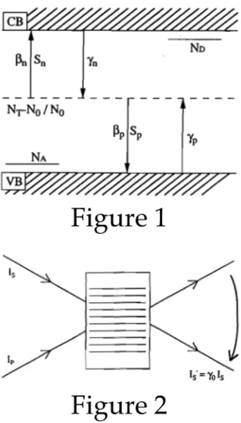
The expression of the photoinduced space-charge field is derived following the band transport model 8,9 with a single defect in a
concentration NT which ionized part is in concentration N0 and neutral part
in concentration NT-N0 (Fig.1). We consider both thermal (ß) and optical
(S) emission of electrons and holes from the defect. The illumination is given by a spatially modulated interference pattern along coordinate axis z,
I = I0 1+ Re m e ikz
(
)
(
)
with a wave number k (k = 2!" , ! = "
2 n0 sin#
grating spacing with θ the half-angle between the two interfering beams inside the crystal, n0 is the linear refractive index of the material, and λ the
wavelength), a modulation m and a total incident illumination I0. In first
approximation the space-charge field is spatially modulated with the same grating spacing than the illumination pattern and, when the stationary regime is reached, its amplitude is (for grating spacing smaller than the diffusion length of the carriers and no applied electric field) :
E1 = ! i mkBT e k 1+ k 2 k02 "0 (1) !0 = Sn
(
NT " N0)
" Sp N0 AnSn(
NT " N0)
+ ApSp N0is the electron-hole competition coefficient, with An = !n+ SnI0 SnI0 and Ap =!p+ SpI0 SpI0 , kBT e ! 0.025eV .
!n = Sn
(
NT " N0)
(resp. !p = SpN0) corresponds to the part of absorptionthat generates electrons (resp. holes). Note that for generation of electrons only (or holes only) !0 is maximal (≈ ±1).
k02 = e
2
! kBT
Neff is the inverse squared of the Debye screening length with
the effective trap density Neff = N0
(
NT ! N0)
NT (ε is the dielectric constant).
E1 is purely imaginary , which means that the space-charge field
grating is π/2-shifted from the illumination grating.
Through the linear electrooptic effect (Pockels effect), the space-charge field grating gives rise to an index grating of amplitude 10 :
!n = n0
3
reff E1
2 (2)
reff is the effective electrooptic coefficient which depends on the orientation
of the sample and on polarization of beams 11. For example in the classical
beam-coupling configuration, i.e. grating vector along [001], propagation along [1 10] and beam polarization along [110], for crystal of the 4 3m class of symmetry such as GaAs, InP or CdTe, we have reff =r41.
The diffraction of the two beams on the index grating they create, gives an energy transfer from one beam to the other one 8. This two wave
mixing (TWM) process is characterized by a photorefractive gain Γ : ! = 2" n0 3 r 4 1 # cos$ kBT e k 1+ k 2 k02 %0 (3)
Experimentally the energy transfer is measured as the ratio γ0 of the
intensity of a probe beam with and without the presence of a coherent pump beam (Fig.2). In the condition of high pump-to-probe beam ratio (i.e. small modulation of the fringes), γ0 is written :
!0 = e" l (4)
TWO BEAM COUPLING IN SEMIINSULATING GaAs : A QUANTITATIVE EXAMPLE
We now present, as an illustration, photorefractive experiments performed on a well characterized semiconductor : semiinsulating undoped GaAs. The PRE is analyzed through a TWM experiment in which we measure the energy transfer from a pump beam to a probe beam as a function of the grating wavenumber k. This is achieved at the two wavelengths 1.06µm and 1.32µm given by CW diode-pumped Nd-YAG lasers. From the measurement of the effective gain γ0 (Fig.2), we deduce
photorefractive gain Γ (Fig.3) according to expression (4). The results are analyzed using equation (3), in which the extrinsic material properties are contained in the electron-hole competition coefficient !0 and Neff the deep
level effective trap density (i.e. k02).
In LEC grown undoped GaAs the semiinsulating character of the material is due to the compensation of the residual shallow donors and acceptors, with concentrations NA>ND≈1015cm-3, by the intrinsic EL2
defect (NEL2 ≈ 1...2x1016 cm-3) 12, which gives rise to a deep 0/+ level at
0.75eV below the bottom of the conduction band 13. EL2 defect is an
arsenic-antisite related double donor defect. The electrical compensation and, related with this, the atomic structure of the EL2 defect have been the object of numerous studies and recent reviews are available 14. Whereas the
total EL2 concentration is relatively constant, around 2x1016cm-3 for high
pressure LEC grown materials, the occupation ratio EL2
[
+]
/ EL20[
]
depends on the crystal growth conditions and on parameters such as the purity of the starting materials or the humidity of the encapsulation but equally on the position in the ingot. Occupation ratio between 1 and 0.1 can be found, but modern state of the art material optimized as substrate materials for microelectronics applications is characterized by a value of about 0.1. The EL2 defect, which is at the origin of the electrical compensation, is equally responsible for the photoconductivity in the 1-1.5µm spectral range 15 due to the optical cross sections Sn and Sp of
EL20 and EL2+ respectively, which are both of importance at these
excitation energies. The determination of the absolute values of these cross sections at room temperature has only been achieved recently 16.
The quantitative analysis of the TWM experiment requires further the knowledge of the absolute concentrations of EL20 and EL2+; the values
can either be obtained by an all optical absorption measurement at two different wavelengths 17 or by the application of the electron paramagnetic
resonance (EPR) technique concerning EL2+ 18. The application of this last
technique is generally preferable due to its defect selective character, whereas the quality of an absorption measurement depends strongly on the absence of other deep levels. The EPR spectrum (Fig.4) of the EL2+ defect
is described by the Spin Hamiltonian :
H = gßBS + AIS (5)
with the Landé factor g=2.04 and the central hyperfine interaction constant A= 890x10-4cm-1, both isotropic (with ß the Bohr magneton and B the
magnetic field, S=1/2 is the electronic spin and I=3/2 is the nuclear spin) . The spin concentration is obtained by a double integration of the experimental first derivative spectrum and a comparison with a spin standard sample.
With the help of the concentrations determined in the sample from absorption measurement for EL2
[
0]
and from EPR measurements forEL2+
[
]
, as well as the other parameters taken from the literature 16,19,20 wecalculate the photorefractive gain (Fig.3). We find a good agreement between calculated values and the experimental ones, thus confirming the model for the photorefractive effect. The change of the sign of photorefractive gain from λ=1.06µm to λ=1.32µm, indicates a change of the majority carrier for PRE. These curves have been obtained for a GaAs sample in which the compensation ratio EL2+
[
]
/ EL2[
0]
is close to one. Thus the sign reversal for !0 follows the variation of the Sn/Sp ratio withwavelength (Sn/Sp >1 for λ=1.06µm ; Sn/Sp > for λ=1.32µm 16).
The importance of the electron-hole competition in PRE experiments is well illustrated by these results : in particular at the wavelength of 1.32µm the electron-hole competition is very sensitive to the compensation ratio due to the increasing importance of Sp over Sn. Thus a sample with a
ratio EL2+
the gain between 1.06µm and 1.32µm contrary to this sample, this is what we indeed observed in our experiments. It becomes further clear that materials optimized for applications at 1.06µm are not necessarily suited for applications at 1.5µm. The optimization of the performances of GaAs at different wavelengths thus requires materials with different compensation ratios ; these can in principle be adapted by the growth conditions, but as currently semiinsulating GaAs is grown for microelectronics applications such material is not available on the market. A second approach would be to modify the compensation by post growth treatments such as electron irradiation or thermal treatments 21,22.
A COMPARISON OF INFRARED ACTIVE MATERIALS
The evaluation of photorefractive performances of a material can be assessed through different criteria, such as the required irradiance, the electron-hole competition rate, the effective trap density or the refractive index change. We will now precise all these points.
In insulating materials, we usually consider that the steady-state value of the PRE does not depend on the incident illumination, which only affects the time constant at which the steady-state is reached. In semiconductors, this is a little more complex due to the semiinsulating nature of the material. Carriers can be excited from the deep level either optically or thermally. The thermal emission is not spatially modulated and its effect will be an isotropic redistribution of charges that will decrease the strength of the space charge field. This influence is expressed by the terms An and Ap in the
ξ0 expression (1). In a one carrier model (for example electrons), the
! = !"
1+ #n Sn I0
(6)
Γ∞ is the photorefractive gain obtained at an irradiance giving a number of
photoexcited carriers larger than the thermally excited one : SnI0 >> ßn, i.e.
An=1. At low irradiance the gain is reduced due to the influence of ßn. We
define the equivalent dark irradiance Id as the irradiance for which the gain
is reduced by a factor 2. It corresponds, in a one defect model, to : SnId = ßn.
In semiconductors with a monopolar conduction, the conductivity is defined as : ! = !d +!p h = e µn "n
(
NT # N0)
$nN0 + e µn Sn(
NT # N0)
$n N0 I0 (7)where µn (µp) is the electron (hole) mobility, and γn (γp) the recombination
coefficient of electrons (holes). This means that Id can be defined as the
irradiance for which photoconductivity σph equals dark conductivity σd. In a
bipolar model, Id can always be defined but its relation to conductivity is not
as simple. Nevertheless, the comparison of photoconductivity and dark conductivity gives a good clue to the illumination dependence of photorefractive gain. We thus have a first criteria for the performance of a photorefractive crystal : the photoconductivity must overpass the dark conductivity. This condition gives the minimal irradiance at which a crystal can be effectively used (i.e. An= Ap=1).
The second important point is the electron-hole competition factor :
!0 =
Sn
(
NT " N0)
" SpN0 Sn(
NT " N0)
+ SpN0(8)
This coefficient varies between -1 and 1, the optimum condition being !0 = 1, i.e. monopolar case. The sign of ξ0 gives the majority carrier for
PRE : electrons correspond to ξ0>0, (holes to ξ0<0). In the case of an exact
compensation (i.e. Sn(NT -N0) =SpN0 ), the photorefractive gain equals zero.
A good photorefractive crystal should be the closest as possible to the monopolar case in order to exhibit high gains. This parameter is often hard
to modify by post growth treatments as discussed above on the example of GaAs. For a fixed wavelength and a given defect only a modification in the compensation ratio (NT-N0)/N0 can help to change the electron-hole
competition. This implies a good control of the Fermi level in the as-grown crystals. As the optical cross sections Sn and Sp depend on the photon
energy we have for each case an optimum wavelength ; however for practical reasons the wavelengths are fixed and this parameter can not be varied freely. Different doping can equally help to change the range of utilization of a given material. In all cases it is necessary to characterize quantitatively the defect relevant for the PRE.
The third criteria deals with the effective trap density Neff. This
quantity gives the maximum number of charges that can be redistributed and then the maximum space-charge field that can be induced. For a defect under two states of charge, Neff is given by the minority species, which
means that even if a high defect concentration is obtainable, care as to be taken in the control of the compensation ratio of the material. Note that an increase of the concentration of the defect (by higher doping for example) also increases α the absorption of the crystal.
The last point to fully characterize the induced index change is given by the parameter n03 r4 1. The higher n03 r4 1, the higher the photorefractive
gain. This gives for example an argument in favor of II-VI semiconductors for which n03 r4 1 is twice higher than for III-V materials.
Three materials are widely used for PRE in the infrared : undoped GaAs 3,5,23, Iron doped InP 3,24,25 and more recently Vanadium doped
CdTe 4,26,27. Their characteristics are presented in Table1. Some other
semiconductors are also studied (GaP 33, ZnTe 34, CdSe 35) but they are
mainly developed for their properties in the visible even if some (ZnTe) have sensitivity which extends towards 1.32µm. Another possibility is the
extension to alloys 36, such as CdZnTe or CdMnTe which allow a choice of
the band gap value and then a possible adjustment of some of their properties.
If we look at Table 1, keeping in mind the four important criteria for performances previously defined, we see that CdTe has the higher index change due to its higher electrooptic coefficient. Its sensitivity range extends beyond 1.5µm. GaAs is the crystal that possess the highest photoconductivity but, as discussed previously, the important point is the ratio between dark conductivity and photoconductivity. According to this criteria CdTe can be used with lower irradiance (of the order of 0.1mW.cm-2). Working with extrinsic semiconductors, the dark
conductivity is related to the defect, giving rise to the Fermi level pinning. This Fermi level pinning can lead to dark conductivity close to the intrinsic conductivity, determined by the energy band gap of the material. For example, undoped Bridgman CdTe is n-type conductive and then unsuitable for photorefractive applications; it is the vanadium doping which leads via a deep V0/+ donor level and non identified acceptors to high resistive and
photoconductive material 37.
The highest photorefractive gain without applied electric field is obviously obtained in CdTe due to its higher electrooptic coefficient. When considering results currently obtained under applied DC field, the highest gains were obtained in InP:Fe. Indeed a resonant enhancement is achieved when photogeneration of holes and thermal emission of electrons equal each other 25. This technique, only demonstrated for InP:Fe, requires an accurate
control of both illumination and temperature. Classical techniques use either DC field and moving gratings 23 or AC field. This last techniques are
currently developped in CdTe to obtain high photorefractive gains 27,32.
Application of high electric fields raise equally the problem of suitable electrical contacts, homogeneity of the field distribution inside the crystal
and the fact that defect properties can be sensitive to the electric field strength. This last point for example is of importance for the EL2 defect in GaAs 38. The field dependent capture cross section of EL2 39 leads, for
fields above 300V.cm-1, to the formation of moving high field domains.
These problems may impede the use of GaAs in applications requiring external applied fields.
According to the values in Table 1, CdTe seems to be the most promising crystal for use in the 1.3-1.5µm spectral range with low power laser diodes. However the defect properties of CdTe:V are much less known than those of III-V semiconductors and more studies are required and are currently under way in various laboratories in order to optimize CdTe:V for PRE applications.
CONCLUSION
The main particularity of the photorefractive effect, that makes it attractive for beam processing, is an optical nonlinearity leading to efficient energy transfer and phase conjugation with low power lasers. The materials that are sensitive in the near infrared are the semiinsulating semiconductors. Good correlation is obtained between the theoretical model describing the PRE and experimental results in that kind of crystals. This points out a possible use of the PRE as a characterization technique of deep levels in these materials which are of importance as substrates for microelectronics. For optical processing applications in the near infrared, optimization has still to be continued in order to obtain an optimum effect for specified wavelengths. Nevertheless the magnitude of the effects already obtained has lead to the beginning of device realizations in different research groups.
An example of such a device is the Double Phase Conjugate Mirror (DPCM) 40. The DPCM allows to couple two mutually incoherent beams
and to create their phase conjugates. The great interest of such a device is that the temporal information of one beam is transferred to the phase conjugate of the other beam. Consequently, a DPCM can realize a wavefront conversion of a beam having an arbitrary wavefront into a beam with a perfect wavefront. That makes this device important for beam processing in free space telecommunication systems. High gain are necessary to overpass the threshold of devices like DPCM ( ! " #
(
)
l > 4 ), which means that we are in search for a crystal that presents high photorefractive gain in the spectral range 1.3-1.5µm with the low energies given by laser diodesREFERENCES :
[1] A.Ashkin, G.D.Boyd, J.M.Dziedzic, R.G.Smith, A.A.Ballman, H.J.Levinstein, K.Nassau, Appl. Phys. Lett. 9 (1966) p.72
[2] P.Günter, J.P.Huignard, Photorefractive materials and their applications I and II Vol 61-62 ( Springer Verlag, 1988).
[3] A.M.Glass, A.M.Johnson, D.H.Olson, W.Simpson, A.A.Ballman, Appl. Phys. Lett. 44 (1984) p.948
[4] R.B.Bylsma, P.M.bridenbaugh, D.H.Olson, A.M.Glass, Appl. Phys. Lett. 51 (1987) p.889
[5] M.B.Klein, Opt. Lett. 9 (1984), p.350.
[6] R.B.Bylsma, D.H.Olson, A.M.Glass, Appl. Phys. Lett. 52 (1988) p.1083
[7] K.Jarasiunas, Ph.Delaye, G.Roosen, Phys. Stat. Sol. B175 (1993) p.445
[8] N.V. Kukhtarev, V.B. Markov, S.G. Odulov, M.S. Soskin, V.L. Vinetskii, Ferroelectrics 22 (1979) p.949; 22 (1979) p.961.
[9] F.P. Strohkendl, J.M.C. Jonathan, R.W. Hellwarth, Opt. Lett. 11 (1986), p.312.
[10] H. Kogelnik, Bell. System. Technical. Journal. 48 (1969) p.2909. [11] J. C. Fabre, J.M.C. Jonathan, G. Roosen, Opt. Comm. 65 (1988), p.257.
[12] G.M.Martin, J.P.Farges, G.Jacob, J.P.Hallais, G.Poiblaud, J.Appl. Phys. 51 (1980) p.2840
[13] E.J. Johnson, J.A. Kafalas, R.W. Davies. J. Appl. Phys. 54 (1983), p.204.
[14] See for example : J.C.Bourgoin, H.J.Von Bardeleben, D.Stiévenard. J. Appl. Phys. 64 (1988), p.R65.
[16] P.Silverberg, P.Omling, L.Samuelson. Appl. Phys. Lett. 52 (1988), p.1689.
[17] F.X. Zach, A. Winnacker. Jap. J. Appl. Phys. 28 (1989), p.6.
[18] R.J. Wagner, J.J. Krebs, G.H. Strauss, A.M. White. Sol. State Commun. 36 (1980), p.15.
[19] D.T.F. Marple, J. Appl. Phys. 35 (1964), p.1241.
[20] C.A. Berseth, C. Wuethrich, F.K. Reinhart, J. Appl. Phys. 71 (1992), p.2821.
[21] Ph. Delaye, H.J. Von Bardeleben, G.Roosen, in Digest of Topical Meeting on Photorefractive Materials, Effects and Devices IV (6-10 august 1993, Kiev) Paper FrC02.
[22] L.J.Cheng, J.Lagowski, M.F.Rau, F.C.Wang. Radiation Effect And Defect In Solid 111 (1989), p.37
[23] B. Imbert, H. Rajbenbach, S. Mallick, J.P. Herriau, J.P. Huignard, Opt. Lett. 13 (1988) p.327.
[24] P. Delaye, P. U. Halter, G. Roosen, J. Opt Soc. Am. B 7 (1990), p.2268 .
[25] G. Picoli, P. Gravey, C. Ozkul, V. Vieux.J. Appl. Phys. 66 (1989), p.3798.
[26] J.C.Launay, V.Mazoyer, M.Tapiero, J.P.Zielinger, Z.Guellil, Ph.Delaye, G.Roosen, Appl. Phys. A 55 (1992), p.33.
[27] M.Ziari, W.H.Steier, P.M.Ranon, M.B.Klein, S.Trivedi, J.Opt.Soc.Am.B 9 (1992) p.1461.
[28] N. Suzuki, .K. Tada, Jpn. J. Appl. Phys. 23 (1984) p.291. [29] D.T.F. Marple, J. Appl. Phys. 35 (1964), p.539.
[30] D.T.H.Liu, L.J.Cheng, M.F.Rau, F.C.Wang, Appl. Phys. Lett. 53 (1988) p.1369
[31] C.Ozkul, G.Picoli, P.Gravey, N.Wolffer, Appl. Opt. 29 (1990) p.2711.
[32] Y.Belaud, P.Delaye, J.C.Launay, G.Roosen, accepted for publication in Opt.Commun. (1993)
[33] K. Kuroda, Y. Okazaki, T. Shimura, H.Okamura, M. Chihara, M. Itoh, I. Ogura, Opt. Lett. 15 (1990) p.1197.
[34] M.Ziari, W.H.Steier, P.M.Ranon, S.Trivedi, M.B.Klein, Appl. Phys. Lett. 60 (1992), p.1052.
[35] P.Tayebati, J. Kumar, S.Scott Appl. Phys. Lett. 59 (1991), p.3366. [36] M.Ziari, W.H.Steier, M.B.Klein, S.Trivedi, in Digest of Topical Meeting on Photorefractive Materials, Effects and Devices III (August 1991, Beverly) Paper TuA6.
[37] H.J. Von Bardeleben, J.C.Launay, V.Mazoyer, Appl. Phys. Lett. 63 (1993), p.1140.
[38] G.C.Valley, H.Rajbenbach, H.J.Von Bardeleben, Appl. Phys. Lett. 56 (1990), p.364.
[39] M. Kaminska, J.M. Parsey, J. Lagowski, H.C. Gatos, Appl. Phys. Lett. 41 (1982), p.989.
FIGURE CAPTIONS :
Fig.1 : Energy diagram of semiconductors as a function of a space coordinate. For symbol definition, see text
Fig.2 : Two wave mixing scheme showing energy transfer from the pump beam Ip to the probe beam Is.
Fig.3 : Photorefractive gain Γ as a function of the grating wave vector k. The experimental curves show results for λ=1.06µm (+) and for λ=1.32µm (×). Straight and dashed lines represent theoretical curves.
Fig.4 : EPR spectrum of the EL2 defect.