HAL Id: hal-02406102
https://hal.archives-ouvertes.fr/hal-02406102
Submitted on 19 Nov 2020HAL is a multi-disciplinary open access
archive for the deposit and dissemination of sci-entific research documents, whether they are pub-lished or not. The documents may come from teaching and research institutions in France or abroad, or from public or private research centers.
L’archive ouverte pluridisciplinaire HAL, est destinée au dépôt et à la diffusion de documents scientifiques de niveau recherche, publiés ou non, émanant des établissements d’enseignement et de recherche français ou étrangers, des laboratoires publics ou privés.
Correlative investigation of Mg doping in GaN layers
grown at different temperatures by atom probe
tomography and off-axis electron holography
Lynda Amichi, Isabelle Mouton, Victor Boureau, Enrico Di Russo, Philippe
Vennegues, Philippe de Mierry, Adeline Grenier, Pierre-Henri Jouneau,
Catherine Bougerol, David Cooper
To cite this version:
Lynda Amichi, Isabelle Mouton, Victor Boureau, Enrico Di Russo, Philippe Vennegues, et al.. Cor-relative investigation of Mg doping in GaN layers grown at different temperatures by atom probe tomography and off-axis electron holography. Nanotechnology, Institute of Physics, 2020, 31 (4), pp.045702. �10.1088/1361-6528/ab4a46�. �hal-02406102�
Correlative investigation of Mg doping in GaN layers
grown at different temperatures by atom probe
tomography and off-axis electron holography
Lynda Amichi,
†Isabelle Mouton,
‡Victor Boureau,
‡Enrico Di Russo,
‡Philippe
Vennéguès,
¶Philippe De Mierry,
¶Adeline Grenier,
‡Pierre-Henri Jouneau,
†Catherine Bougerol,
§and David Cooper
∗,‡Univ. Grenoble Alpes, CEA, INAC, F-38000 Grenoble, France, Univ. Grenoble Alpes, CEA, LETI, F-38000 Grenoble, France, CRHEA-Nice, Rue Bernard Grégory, Les Lucioles
1, 06560 Valbonne, France, and Univ. Grenoble Alpes, CNRS, Institut Néel, F-38000 Grenoble, France
E-mail: david.cooper@cea.fr
KEYWORDS: Gallium nitride, doping, Mg-clusters, laser-assisted atom probe tomogra-phy, off-axis electron holography
∗To whom correspondence should be addressed
†Univ. Grenoble Alpes, CEA, INAC, F-38000 Grenoble, France ‡Univ. Grenoble Alpes, CEA, LETI, F-38000 Grenoble, France
¶CRHEA-Nice, Rue Bernard Grégory, Les Lucioles 1, 06560 Valbonne, France §Univ. Grenoble Alpes, CNRS, Institut Néel, F-38000 Grenoble, France
Abstract
Correlation between off-axis electron holography and Atom Probe Tomography (APT) provides morphological, chemical and electrical information about Mg-doping (p-type) in gallium nitride (GaN) layers that have been grown at different temperatures at a nanometric scale. APT allows access to the 3-Dimensional (3D) distribution of atoms and their chemical nature. In particular, this technique allows visualisation of the Mg-rich clusters observed in p-doped GaN layers grown by Metal-Organic Chemical Vapour Deposition (MOCVD). As the layer growth temperature increases, the cluster density decreases but their size indicted by the number of atoms increases. Moreover, APT reveals that threading dislocations are decorated with Mg atoms. Off-axis elec-tron holography provides complementary information about the electrical activity of the Mg-doping. As only a small fraction of dopant atoms are ionized at room tem-perature, this fraction is increased by annealing the specimen to 400 ◦C in-situ in a Transmission Electron Microscope (TEM). A strong reduction of the dopant electrical activity is observed for increases in the layer growth temperature. The correlation of APT with TEM-based techniques was shown to be a unique approach in order to inves-tigate how the growth temperature affects both the chemical distribution and electrical activity of Mg dopant atoms.
The control of p-type doping is necessary for the production of high performance devices based on III-nitride materials. Mg is currently the only efficient p-type dopant, but it has a high ionisation energy of ∼250 meV, meaning that only ∼1 % of the dopants are active at room temperature.1 Therefore, the incorporation of very high dopant concentration (>
1020cm−3) is necessary in order to achieve a high enough hole concentration ( > 1018cm−3).2
Unfortunately, when using growth techniques performed at high temperatures such as Metal-Organic Chemical Vapour Deposition (MOCVD), as the Mg concentration increases above 2×1019 cm−3 then the generated hole concentration can saturate and then decrease drasti-cally.3 Two main explanations have been proposed for this phenomenon. The first being the
formation and increase of complexes such as MgVN, acting as compensation centres.4 The
second being the formation of Pyramidal Inversion Domains (PIDs), whose density increases with Mg concentration. The boundaries of these PIDs are believed to be formed of Mg3N2
where Mg atoms are electrically inactive.2,5 Previous studies of PIDs, which include atomic
resolution imaging, Energy Dispersive X-ray Spectrometry (EDS) and modelling, suggest that Mg-rich inversion domain boundaries form on (0001) planes and these may include a significant fraction of the Mg dopant atoms.6–8 Besides the problem of the Mg acting as a deep acceptor, there are many additional parameters that impact on the efficiency of the p-GaN doping, such as the growth temperature, leading to a deterioration of the overall properties of the optoelectronic devices.9,10 For these reasons the dopant atom distribution
and its electrical activity must be investigated with a nm-scale spatial resolution to better understand the sample electrical properties.
In order to directly investigate the influence of the growth temperature on both the distribution and activity of the Mg dopant atoms, a dedicated sample containing several p-type GaN layers grown by MOCVD at different temperatures in the range 970 - 1090 ◦C was investigated. Figure 1(a) shows a schematic of the sample. This consists of a stack of 65 nm thick Mg-doped GaN layers alternated with 130 nm thick Non-Intentionally Doped (NID) GaN layers. A lamella specimen and atom probe needle-shaped tips were prepared
using a standard lift out procedure using a Scanning Electron Microscope/Focused Ion Beam (SEM/FIB) operated at 16 kV.11,12
High-Angle Annular Dark Field Scanning Trasmission Electron Microscopy (HAADF-STEM) was performed using a double aberration corrected FEI Titan Ultimate operated at 300 kV. Figure 1(b) shows a HAADF-STEM image of a cross section of the lamella specimen observed down the [11¯20] zone axis. The laters with brighter contrast correspond to p-GaN layers grown at higher temperatures. Such contrast arises from a "halo" around the PIDs which becomes clearly visible from 1030 ◦C. Figure 1(c) shows a magnified region of the layer grown at 1090 ◦C. The presence of several triangular shaped PIDs is observed. One of these is shown with atomic resolution in figure 1(d). Finally, the size of the base of 15 different PIDs was measured for each growth temperature. Results are reported in Figure 1(e). These reveal an increase in the size of PIDs from (1.9 ± 0.4) to (3.9 ± 0.7) nm for growth temperatures ranging from 1030 to 1090 ◦C, respectively.
Although the STEM data provides useful information about the morphology (i.e. the size of the PIDs), it is difficult to map the Mg distribution in the doped layers due to the low atomic concentrations that are present. To obtain information about the 3D distribu-tion of the Mg atoms inside and outside the PIDs, Atom Probe Tomography (APT) was performed. A needle-shaped specimen was analysed using a CAMECA FlexTAP. The anal-ysis parameters were optimized to operate at low electric field condition on the tip surface and thus to observe the best signal-to-noise ratio in the mass spectrum.13,14 This reduces
also the preferential loss of metallic species during the tip evaporation and allows to better estimate the Mg fraction.15,16 The 3D reconstruction was performed using a cone-angle
al-gorithm. As it was not possible to properly reconstruct the entire volume analyzed adopting a unique set of parameters, different sub-volumes containing a single p-doped layer was sep-arately reconstructed. More information regarding the APT analysis conditions and the 3D reconstruction are reported in Supplementary Information.
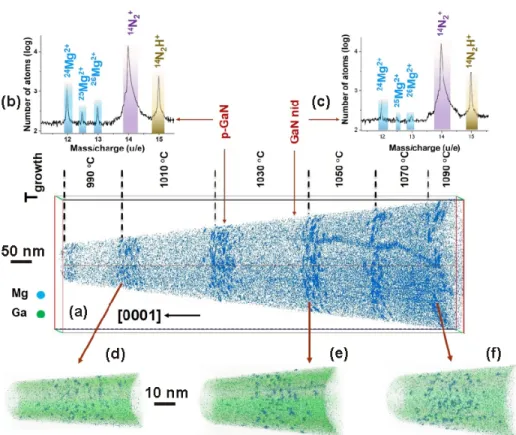
The APT 3D reconstruction of the entire volume analysed is shown in Figure 2(a). The layers grown from temperatures of 990 ◦C to 1090 ◦C can be identified by the Mg distribu-tion. The top layer grown at 970 ◦C was not considered here, due to FIB damaging during preparation. Figures 2(b-d) show three examples of reconstructed sub-volumes at different growth temperatures. The mass spectra extracted from two different regions of the specimen shown in Figure 2(a) reveal that Mg atoms are present in p-doped layers, but also in the NID ones, which is likely due to the surfactant properties of Mg during growth. Mg naturally occurs in three isotopes, forming peaks at 12, 12.5 and 13 Da in atom probe mass spectra. Nevertheless, in the NID layers only the principal isotope (24Mg) can be clearly distinguished
at 12 Da (Figure 2(a)) indicating that in these layers the Mg concentration is close to the APT detection limit.
The capability of APT to provide 3D images at an atomic scale and clearly identify the chemical nature of atoms in the reconstruction is a key point for the identification of Mg-enriched regions embedded in the GaN matrix. However, current limitations in the technique do not allow the structure of the Mg atoms within the PIDs to be resolved. The triangular Mg-enriched regions associated to PIDs are identified from the formation of Mg clusters in the 3D reconstruction (Figure 2(a)). Mg clustering is observed in all the doped layers grown from 990◦C to 1090◦C, in agreement with previous APT analyses.17,18These Mg rich regions
are likely related to the PIDs observed by TEM. However, despite Mg atoms are present in the NID layers, no Mg clusters are observed. Moreover, APT reveals also that threading dislocations are decorated with Mg atoms (Figure 2(a)). The presence of Mg at hollow cores of both edge and mixed dislocations have been already reported from respectively TEM19 and STEM20analyses. According to molecular dynamics calculations, these Mg atoms would occupy interstitial sites21 and therefore would not behave as acceptors.
From the 3D reconstruction of the doped layers, a cluster identification was performed using the maximum separation distance technique based on the calculation of distance be-tween first nearest neighbour of solute atoms.22,23 Then, from this identification, the number
of Mg atoms can be determined inside each cluster as well as the overall cluster density inside each p-doped layer. The results are shown in Figure 3(a). The data reveals that the size of the clusters, indicated by the number of Mg atoms detected, increases whereas the cluster density decreases with increasing growth temperature. The latter behaviour is consistent with the HR-STEM analysis performed on the PIDs (cfr. Figure1(e)). Note that the layer grown at 990 ◦C is not considered in this analysis since the evaporation conditions at the beginning of the atom probe analysis were not yet optimized (see Supplementary Information).
APT was also useful to reveal the very small clusters in the 1010 ◦C layer which are not detected by the STEM imaging. On the other hand, the APT Mg fraction profiles through these clusters do not suggest a decrease in Mg at their centres, which would be expected if Mg atoms segregated at the surface of the PIDs.17,24 This effect could be due to the limited
in-plane spatial resolution of APT, but also to differences in the evaporation field between the Mg clusters and the GaN matrix. This generates local magnification aberrations, which can lead to biased local composition in the clusters adding to distortions of their morphology.25 Moreover, due to the well know detection limitations in APT, the number of both Ga and Mg atoms inside clusters is systematically underestimated and is not representative of the number of atoms really present.16 However, as the evaporation conditions were the same for
all layers, the evolution of both clusters size and composition is considered reliable.
Besides providing information about clusters, APT has the unique capability to estimate also the Mg fraction y = M g+GaM g that are present outside of the clusters and within the GaN matrix. These Mg atoms are considered to be potentially electrically active. In order to do this, Mg atoms present in either clusters or other defects, such as threading dislocations, were not considered because are supposed to be electrical inactive. Of course, the measured fraction y within a layers is not strictly quantitative and is only used to demonstrate the relative evolution of the composition.15,16,26 The Mg fraction for both the potentially active
different growth temperatures. The Mg concentration in the layers rapidly decreases from 1010 ◦C to 1050 ◦C and then stabilizes, while in the NID layers it remains constant with a slight increase for the layer grown at the highest temperatures (1070◦C - 1090 ◦C).
The chemical information obtained from APT cannot be directly connected with the electrical activity of dopant atoms. For this reason, off-axis electron holography was per-formed. This allows the measurement of the electrostatic potential and the determination of the relative electrical activity in the different layers as a function of growth temperature. Off-axis electron holography technique is a TEM based technique that uses an electron biprism to create an interference pattern known as the hologram.27A coherent electron wave
that passes through the specimen is interfered with another that passes through vacuum. From a Fourier reconstruction procedure, information about the phase of these electrons can be retrieved. In the absence of dynamical diffraction and magnetic fields, the measured phase is sensitive to the local electrostatic potential of the active dopants Vdopant and the
Mean Inner Potential (MIP) VM IP. The phase change ∆φ(x, y) of an electron that passes
through a specimen is given by;28
∆φ(x, y) = CE
Z t
0
VE(x, y, z)dz, (1)
where: VE(x, y, z)=VM IP + Vdopant; the constant CE is dependant on the operating
voltage of the TEM which equals to 0.0073 rad · nm-1 V -1 for 200 kV electrons and t is
the thickness of the specimen. The value of the VM IP for GaN was calculated by Density
Functional Theory (DFT) and is found to be 16.8 V.29
It is known that the surfaces of the TEM specimens do not act in the same manner as the bulk when examining electric potentials. Firstly, this is due firstly to FIB damage, which can be reduced with a low FIB operating voltage. Secondary, the band bending at the top and bottom surfaces of the TEM specimen due to surface states leads to values of potential less than expected.30–33 Systematic studies of doped Si and GaAs p-n junctions shows that
inside the TEM specimen.30,31 As such, it is necessary to look at relatively thick specimens to minimise these effects, especially for low active dopant concentrations. thirdly, in GaN the generated current during the interaction with the electron beam may add an additional contribution acting as a forward bias.34 Previous studies on doped GaN specimens have
shown that the measured potential is in the range of 0.4 to 0.5 V instead of the expected value of 3.4 V.34 In Si and GaAs p-n junctions the correct potentials can be recovered when high dopant concentrations are examined and by the application of good electrical contacts to remove the build up of charge from the electron beam. Thus the experiments must be performed using a low electron beam intensity. Of course, the observation of thick specimens using low beam intensities leads to very noisy phase images. To solve this problem, series of holograms were acquired and summed to provide improved signal-to-noise. Because all these artefacts are reduced for higher active dopant concentrations, the specimen was heated in-situ in the TEM in order to increase the concentration of the ionised Mg dopants.32 At
room temperature, a thermally ionized Mg dopant concentration of ∼ 1.2 % is expected (cfr. Equation 3 in the Supplementary Information). Therefore, the specimen was examined at 400 ◦C to increase this concentration to a theoretical value of ∼ 14%.
Off-axis electron holography was performed using a Cs probe corrected FEI Themis TEM operated at 200 kV, using a Lorentz lens to provide a large field of view. A biprism voltage of 177 V was used to provide a hologram of 770 nm width with a fringe spacing of 4 nm. The specimen was mounted in a Gatan double-tilt annealing holder and tilted by 2◦ from the [11¯20] zone axis to reduce diffraction contrast whilst keeping the layers edge-on, such that the measured width of the layers was not affected by this loss of resolution in projection. Two series of 32 holograms, with individual exposure times of 8 s, were acquired at room temperature and at 400◦C using a 2048×2048 pixels CCD camera. High temperatures reduce the artefact effects and increase the measured signal. However, this could lead to significant atomic diffusion, even if the heating temperature is well below the growth one. To verify this, the specimen was re-examined at room temperature after being heated for 6 hours to
confirm that no structural changes or dopant diffusion had occurred. The hologram series were finally reconstructed using the Holoview software which aligns and averages hologram series for improved signal to noise.35 The phase images were reconstructed with a spatial
resolution of 10 nm. Higher spatial resolutions are possible but this is at the expense of the field of view as the interference fringes need to be sampled by at least 6 pixels to maintain a good signal to noise ratio. Reference holograms were then used to remove geometrical distortions from the imaging system.
Figure 4(a) shows the potential map acquired at room temperature. Dark contrast is as-sociated to the p-type regions, bright contrast to the NID regions. The latter would usually be intrinsically n-type due to a residual n-type background, estimated to be 5×1017 cm−3 for
Tgrowth = 780◦C.36 However, Mg atoms were also observed by APT in the NID layers. The
concentration of such p-doping was estimated by Secondary Ion Mass Spectrometry (SIMS) to be 0.6×1019cm−3. Even assuming the unlikely figure of 100 % activity of the p-type Mg in the NID layers, it would still expect these regions to be n-type at room temperature. Figure 4(c) shows the potential profile measured across the indicated region. The step in potential measured between each of the doped and NID layers is shown in Figure 4(d) as a function of growth temperature. A value of (0.40 ± 0.02) V is obtained for Tgrowth = 970 ◦C,
dras-tically decreasing towards higher temperatures. Thus holography provides a clear evidence that the use of higher growth temperatures decreases the electrical activity of the dopant atoms. However, the theoretical step in potential between a p-doped and intrinsic GaN with concentration of acceptors NA= 5×1019cm−3 and donors ND = 5×1017 cm−3 respectively is
approximately 3.4 V at room temperature. This discrepancy between experiment and theory can be explained in part in terms of both FIB damaging and surface charging effects.
In order to reduce the effect of artefacts and increase the measured signal, Vdopant, the
specimen was finally heated in-situ up to 400◦C to increase the ionised dopant concentration. As the A potential map of the specimen at 400 ◦C is shown in Figures 4(b). A potential profile extracted from this map is shown in Figure 4(c). The step in potential between the
layers are finally represented in Figure 4(d) for the two temperatures investigated. This step decreases from (0.51 ± 0.02) V to (0.20 ± 0.02) V for Tgrowth increasing from 970 ◦C to
1010 ◦C, respectively. Then, it reduces to (0.15 ± 0.02) V for Tgrowth = 1090 ◦C. These
values are improved compared to room temperature where the same trend was observed (Figure 4(d)), but they still lower than expected from theory. Further studies are required to understand this discrepancy, although for this sample we should consider the uncertainty from the Mg doping in the NID layers.
The artefacts that are present when measuring the potentials in GaN are currently object of great interest. However, in the case presented here, since all the doped layers are examined within the same TEM specimen, results suggest that a reduction in the step in potential between the layers can be directly interpreted in terms of the relative electrical activity of dopants. This is in agreement with previous studies that observe a decrease in generated holes with growth temperature described as being due to the saturation in the incorporation of the Mg dopant occurring at high growth temperature37 or to the increase of compensation effects.38
Both APT results and HR-STEM observations reveal that as the growth temperature increases, the Mg clusters in the p-doped layers increase in size and become less numerous in the volume. Up to a growth temperature of 1050 ◦C a strong reduction of the Mg fraction outside of the defects (clusters and dislocations) was observed, suggesting a decrease in the generated holes concentration in the p-doped regions. These observations are in agreement with electron holography showing a decrease of the dopant electrical activity in these layers. At temperatures Tgrowth ≥ 1050◦C, APT suggests that, despite the increase in the size of the
PIDs, the number of Mg atoms that are potentially active becomes constant. Meanwhile, the holography results (Figure 4(d)) show a continuous decrease in the electrical activity of the dopant atoms for the different growth temperatures. Correlation of these results suggests that despite it is difficult to directly observe MgVN complexes, these must have a strong
temperatures. More work is required on a range of differently grown specimens to understand whether this trend is universal or particular to this sample that has been studied, and of course better understand how the PIDs and MgVN complexes affect the dopant activity at
the lower growth temperatures.
In conclusion, a correlation between atom probe tomography and off-axis electron holog-raphy has revealed complementary information regarding the distribution and the electrical activity of Mg atoms in GaN layers with nanometer-scale spatial resolution. The growth temperature has a strong impact on the material properties resulting in an increase in the size of clusters that are observed by APT. These are likely associated to the PIDs observed by TEM. The holography shows an strong reduction in the electrical activity of the dopant with the increasing of the growth temperature. A comparison between the trends that are observed from the two techniques suggests that in these samples the MgVN complexes
dom-inate the dopant inactivity at temperatures above 1050◦C whereas at lower temperature the results are more difficult to interpret. For more quantitative interpretation of holography data, a systematic study of a range of differently doped GaN layers is required. This would be used to provide inputs for 3D simulations of the electrostatic potentials in and around the thin TEM specimens which account for the damage introduced by FIB preparation as well as charging on the specimen surfaces which is currently in progress. It is expected that improvements in the analysis of APT data as well as a more effective combination of HR-STEM measurements will allow better determination of the effect of defects such as PIDs and complexes on the doping efficiency in GaN and a wide range of other doped materials.
Supplementary Information
Electron holography
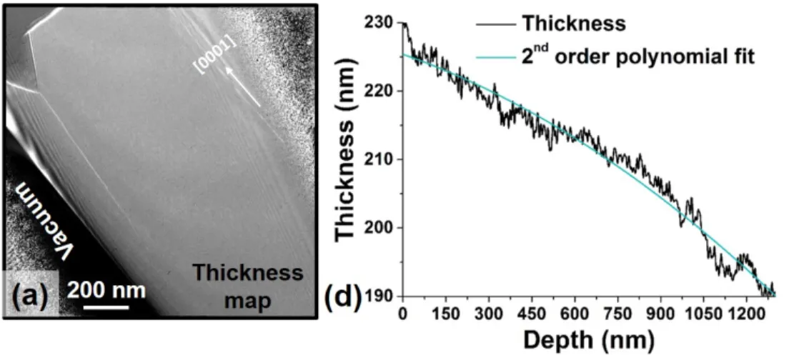
The hologram reconstruction process can be used to calculate an amplitude image from which the specimen thickness can be extracted.28As such, it is possible to correct the effects
of the varying thickness, such that the measured potential is related only to the changes in Vdopant. The thickness map shown in Figure 5(a) was measured directly from the amplitude
image A λt value can be extracted from the following relation:
t
λ = −2 × ln( A0
Ar
), (2)
where: λ is the mean free path; A0 and Ar are the amplitudes of the specimen and
the vacuum, respectively.39 The mean free path can be estimated from the expression,
λ ≈ 106F (
E0 Em)
ln(2βE0Em ) .
40 The value in GaN was measured to be 105 nm in Lorentz mode using
the FEI Titan Themis.
A thickness map from Equation 2 can then be calculated. This is reported in Figure 5(a), also confirming an absence of diffraction contrast across the region of interest which could affect the measured phase. The extracted thickness profile reveals a decrease in the specimen thickness measured to be < 40 nm, which induces a phase gradient due to the MIP phase of approximately 4.7 rad deduced using Equation 1. For this purpose, a 2nd order
polynomial fit of the thickness is used to remove the VM IP component such that the phase
image is directly sensitive to Vdopant.
The hole concentration is directly related to the ionization energy EAand the temperature
T by the charge neutrality equation:
p(p + ND) NA− ND− p = NV g exp(− EA kBT ), (3)
density; ND is the concentration of the residual donors equal to 5×1017 cm−3; kB is the
Boltzmann constant; g the degeneracy of the Mg which is assumed to be equal to 4; NV is
the effective density of states. The ionization energy is estimated at 250 meV.41,42
Atom probe tomography
The experiments were performed using a FlexTAP CAMECA, operated with a UV (344 nm) femtosecond laser. The analysis parameters were the following: field of view: 15◦; tip base temperature: T = 40 K; peak energy density during the laser pulse: ≈ 8×10⁻⁴ nJ · cm−2; constant detection rate: ϕ = 0.002 event/pulse. Data was processed with using Tap3D software from CAMECA. The reconstruction of the whole volume is obtained using a cone-angle algorithm.43 The initial curvature radius was set to 30 nm and the cone angle to 7◦. Due to the large analysed depth (more than 1 micron), it was difficult to reconstruct simultaneously all the Mg doped layers having the same thickness value (65 nm) using just one set of reconstruction parameters and without introducing artefacts.25 Therefore, each
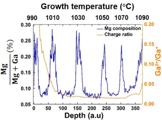
doped layer is reconstructed separately using adapted values of reconstruction parameters (initial radius and cone angle) in order to obtain an approximate nominal thickness of 65 nm. Figure 6 shows the evolution of both the Mg fraction and the Ga Charge-State Ratio (Ga-CSR) GaGa2++ as a function of the specimen depth. Also the corresponding growth temperatures
are reported in figure. The Ga-CSR is observed to strongly decrease at the beginning of the evaporation, then it stabilizes in depth. It varies from 0.07 and 0.05 for layers growth between 1010 ◦C and 1090 ◦C. The so-called effective Field (Fef f) was thus estimated in about 24
V · nm−1 through Kingham0s post-ionization model.44 Precedent studies reveal that such
field conditions lead measuring a more reliable III-fraction in ternary GaN-based alloys.15,16,26
This consideration can also be extended to the case of MgGaN, even if a dedicated study have yet to be developed. Therefore, only information from doped layer grown at Tgrowth= 1010◦C
Figure 1: (a) Schematic of the analysed sample containing layers of undoped and doped GaN grown at different growth temperatures. (b) HAADF-STEM image of the sample. p-type GaN layers appear with bright contrast. A threading dislocation can be observed. (c) Atomic-resolved HAADF-STEM image of the p-type layer grown at 1090◦C. (d) HR-STEM image of a PID in the doped layer grown at 1090 ◦C. (e) PIDs size variation measured by HR-STEM as a function of the growth temperature.
Acknowledgement
Lynda Amichi thanks the GaNeX organisation (ANR-11-LABX-0014) for funding of her Ph.D position. GaNeX belongs to the public funded "Investments d’avenir" program man-aged by the French ANR Agency. David Cooper and Victor Boureau thank the European Research Council for the starting grant Holoview (Stg:306535). These experiments were performed on the Nano-Characterisation Platform (PFNC) at Minatec (Grenoble, France).
Figure 2: APT 3D reconstruction of the analysed tip. (a) 3D distribution of Mg detected atoms in all the evaporated layers including doped and undoped from 990◦C to 1090 ◦C. (b) and (c) are mass spectra in p-doped and NID layers respectively where Mg and its isotopes are identified. (d-f) Reconstructions of three p- doped layers grown at 1010 ◦C, 1050◦C and 1090◦C, respectively. Mg atoms atoms are depicted in blue. Only 1% of the detected Ga atoms are shown in green for a better visibility.
Figure 3: (a) Variation with growth temperature of the number of Mg atoms contained in the clusters and of the clusters density inside each p-doped layer. (b) Variation of the Mg fraction outside of the clusters and also in the NID layers as a function of the growth temperature.
Figure 4: (a) Potential map acquired at room temperature (RT). The p-type layers appear with a dark contrast. (b) Potential map acquired at 400◦C. (c) Potential profiles at room temperature (in black) and 400◦C (in red). (d) Step in potential at room temperature and 400◦C.
Figure 5: (a) Thickness map of the TEM sample showing no diffraction contrast. (b) Thick-ness profile with a 2nd order polynomial fit.
Figure 6: Mg fraction (in blue) and Ga charge-state ratio (in orange), as a function of the sample depth.
References
(1) Zavada, J.; Komirenko, S.; Kim, K.; Kochelap, V. Efficient nitride-based short-wavelength emitters with enhanced hole injection. CONFERENCE SERIES-INSTITUTE OF PHYSICS. 2003; pp 401–404.
(2) Leroux, M.; Vennéguès, P.; Dalmasso, S.; De Mierry, P.; Lorenzini, P.; Damilano, B.; Beaumont, B.; Gibart, P.; Massies, J. Pyramidal defects in highly Mg-doped GaN: atomic structure and influence on optoelectronic properties. The European Physical Journal Applied Physics 2004, 27, 259–262.
(3) Kaufmann, U.; Schlotter, P.; Obloh, H.; Köhler, K.; Maier, M. Hole conductivity and compensation in epitaxial GaN: Mg layers. Physical Review B 2000, 62, 10867.
(4) Remmele, T.; Albrecht, M.; Irmscher, K.; Fornari, R.; Straßburg, M. Pyramidal inver-sion domain boundaries revisited. Applied Physics Letters 2011, 99, 141913.
(5) Vennéguès, P.; Benaissa, M.; Beaumont, B.; Feltin, E.; De Mierry, P.; Dalmasso, S.; Leroux, M.; Gibart, P. Pyramidal defects in metalorganic vapor phase epitaxial Mg doped GaN. Applied Physics Letters 2000, 77, 880–882.
(6) Leroux, M.; Vennegues, P.; Dalmasso, S.; Benaissa, M.; Feltin, E.; De Mierry, P.; Beaumont, B.; Damilano, B.; Grandjean, N.; Gibart, P. Structural Defects and Relation with Optoelectronic Properties in Highly Mg-Doped GaN. physica status solidi (a) 2002, 192, 394–400.
(7) Northrup, J. E. Magnesium incorporation at (0001) inversion domain boundaries in GaN. Applied physics letters 2003, 82, 2278–2280.
(8) Narita, T.; Tomita, K.; Yamada, S.; Kachi, T. Quantitative investigation of the lateral diffusion of hydrogen in p-type GaN layers having NPN structures. Applied Physics Express 2018, 12, 011006.
(9) Krishna, S.; Aggarwal, N.; Mishra, M.; Maurya, K.; Singh, S.; Dilawar, N.; Nagara-jan, S.; Gupta, G. Correlation of growth temperature with stress, defect states and electronic structure in an epitaxial GaN film grown on c-sapphire via plasma MBE. Physical Chemistry Chemical Physics 2016, 18, 8005–8014.
(10) Kushvaha, S.; Pal, P.; Shukla, A.; Joshi, A.; Gupta, G.; Kumar, M.; Singh, S.; Gupta, B.; Haranath, D. Effect of growth temperature on defects in epitaxial GaN film grown by plasma assisted molecular beam epitaxy. AIP Advances 2014, 4, 027114. (11) Padalkar, S.; Riley, J. R.; Li, Q.; Wang, G. T.; Lauhon, L. J. Lift-out procedures for atom probe tomography targeting nanoscale features in core-shell nanowire heterostruc-tures. physica status solidi (c) 2014, 11, 656–661.
(12) Blum, I.; Cuvilly, F.; Lefebvre-Ulrikson, W. Atom Probe Tomography; Elsevier, 2016; pp 97–121.
(13) Di Russo, E.; Blum, I.; Houard, J.; Gilbert, M.; Da Costa, G.; Blavette, D.; Rigutti, L. Compositional Accuracy of Atom Probe Tomography Measurements in GaN: Impact of Experimental Parameters and Multiple Evaporation Events. Ultramicroscopy 2018, (14) Di Russo, E.; Blum, I.; Houard, J.; Da Costa, G.; Blavette, D.; Rigutti, L. Field-Dependent Measurement of GaAs Composition by Atom Probe Tomography. Mi-croscopy and Microanalysis 2017, 23, 1067–1075.
(15) Rigutti, L.; Mancini, L.; Hernández-Maldonado, D.; Lefebvre, W.; Giraud, E.; Butté, R.; Carlin, J.; Grandjean, N.; Blavette, D.; Vurpillot, F. Statistical correction of atom probe tomography data of semiconductor alloys combined with optical spec-troscopy: The case of Al0.25Ga0.75N. Journal of Applied Physics 2016, 119, 105704.
(16) Di Russo, E.; Moyon, F.; Gogneau, N.; Largeau, L.; Giraud, E.; Carlin, J.-F.; Grand-jean, N.; Chauveau, J. M.; Hugues, M.; Blum, I. Composition Metrology of Ternary Semiconductor Alloys Analyzed by Atom Probe Tomography. The Journal of Physical Chemistry C 2018, 122, 16704–16714.
(17) Bennett, S.; Ulfig, R.; Clifton, P.; Kappers, M.; Barnard, J.; Humphreys, C.; Oliver, R. Atom probe tomography and transmission electron microscopy of a Mg-doped Al-GaN/GaN superlattice. Ultramicroscopy 2011, 111, 207–211.
(18) Khromov, D., S.and Gregorius; Schiller, R.; Lösch, J.; Wahl, M.; Kopnarski, M.; Amano, H.; Monemar, B.; Hultman, L.; Pozina, G. Atom probe tomography study of Mg-doped GaN layers. Nanotechnology 2014, 25, 275701.
(19) Cherns, D.; Wang, Y.; Liu, R.; Ponce, F. Observation of coreless edge and mixed dislocations in Mg-doped Al 0.03 Ga 0.97 N. Applied physics letters 2002, 81, 4541– 4543.
Sa-honta, S.-L.; Moram, M. Mg doping affects dislocation core structures in GaN. Physical review letters 2013, 111, 025502.
(21) Harafuji, K.; Kawamura, K. Magnesium diffusion at dislocation in wurtzite-type GaN crystal. Japanese journal of applied physics 2005, 44, 6495.
(22) Philippe, T.; Gruber, F., M.and Vurpillot; Blavette, D. Clustering and local mag-nification effects in atom probe tomography: Astatistical approach. Microscopy and Microanalysis 2010, 16, 643–648.
(23) Gault, B.; Moody, M. P.; Cairney, J. M.; Ringer, S. P. Atom probe microscopy; Springer Science & Business Media, 2012; Vol. 160.
(24) Vennéguès, P.; Leroux, M.; Dalmasso, S.; Benaissa, M.; De Mierry, P.; Lorenzini, P.; Damilano, B.; Beaumont, B.; Massies, J.; Gibart, P. Atomic structure of pyramidal defects in Mg-doped GaN. Physical Review B 2003, 68, 235214.
(25) Gault, B.; Moody, M. P.; Cairney, J. M.; Ringer, S. P. Atom probe microscopy; Springer Science & Business Media, 2012; Vol. 160.
(26) Bonef, B.; Cramer, R.; Speck, J. S. Nanometer scale composition study of MBE grown BGaN performed by atom probe tomography. Journal of Applied Physics 2017, 121, 225701.
(27) Tonomura, A. Electron Holography; Springer, 1999; pp 29–49.
(28) McCartney, M.; Smith, D.; Hull, R.; Bean, J.; Voelkl, E.; Frost, B. Direct observation of potential distribution across Si/Si p-n junctions using off-axis electron holography. Applied physics letters 1994, 65, 2603–2605.
(29) Kruse, P.; Schowalter, M.; Lamoen, D.; Rosenauer, A.; Gerthsen, D. Determination of the mean inner potential in III–V semiconductors, Si and Ge by density functional theory and electron holography. Ultramicroscopy 2006, 106, 105–113.
(30) Cooper, D.; Ailliot, C.; Truche, R.; Barnes, J.; Hartmann, J.; Bertin, F. Experimental off-axis electron holography of focused ion beam-prepared Si p-n junctions with different dopant concentrations. Journal of Applied Physics 2008, 104, 064513.
(31) Cooper, D.; Truche, R.; Twitchett-Harrison, A.; Dunin-Borkowski, R.; Midgley, P. Quantitative off-axis electron holography of GaAs p-n junctions prepared by focused ion beam milling. Journal of microscopy 2009, 233, 102–113.
(32) Cooper, D.; Ailliot, C.; Barnes, J.-P.; Hartmann, J.-M.; Salles, P.; Benassayag, G.; Dunin-Borkowski, R.-E. Dopant profiling of focused ion beam milled semiconductors using off-axis electron holography; reducing artifacts, extending detection limits and reducing the effects of gallium implantation. Ultramicroscopy 2010, 110, 383–389. (33) Somodi, P.; Twitchett-Harrison, A.; Midgley, P.; Kardynał, B.; Barnes, C.;
Dunin-Borkowski, R. Finite element simulations of electrostatic dopant potentials in thin semiconductor specimens for electron holography. Ultramicroscopy 2013, 134, 160–166. (34) Park, J. B.; Niermann, T.; Berger, D.; Knauer, A.; Koslow, I.; Weyers, M.; Kneissl, M.; Lehmann, M. Impact of electron irradiation on electron holographic potentiometry. Applied Physics Letters 2014, 105, 094102.
(35) Boureau, V.; McLeod, R.; Mayall, B.; Cooper, D. Off-axis electron holography combin-ing hologram summation with double-exposure phase shiftcombin-ing : Theory and application. Submitted in Ultramicroscopy 2018,
(36) Tingberg, T.; Ive, T.; Larsson, A. Investigation of Si and O Donor Impurities in Un-intentionally Doped MBE Grown GaN on SiC (0001) Substrate. Journal of Electronic Materials 2017, 46, 4898–4902.
(37) Guha, S.; Bojarczuk, N.; Cardone, F. Mg in GaN: Incorporation of a volatile species at high temperatures during molecular beam epitaxy. Applied physics letters 1997, 71, 1685–1687.
(38) Hurni, C.-A.; Lang, J.-R.; Burke, P.; Speck, J. Effects of growth temperature on Mg-doped GaN grown by ammonia molecular beam epitaxy. Applied Physics Letters 2012, 101, 102106.
(39) Egerton, R. F. Electron energy-loss spectroscopy in the electron microscope; Springer Science & Business Media, 2011.
(40) Malis, T.; Cheng, S.; Egerton, R. EELS log-ratio technique for specimen-thickness measurement in the TEM. Microscopy Research and Technique 1988, 8, 193–200. (41) Kim, D.; Ryu, D.; Bojarczuk, N.; Karasinski, J.; Guha, S.; Lee, S.; Lee, J. Thermal
activation energies of Mg in GaN: Mg measured by the Hall effect and admittance spectroscopy. Journal of Applied Physics 2000, 88, 2564–2569.
(42) Brochen, S.; Brault, J.; Chenot, S.; Dussaigne, A.; Leroux, M.; Damilano, B. Depen-dence of the Mg-related acceptor ionization energy with the acceptor concentration in p-type GaN layers grown by molecular beam epitaxy. Applied Physics Letters 2013, 103, 032102.
(43) Larson, D.; Gault, B.; Geiser, B.; De Geuser, F.; Vurpillot, F. Atom probe tomogra-phy spatial reconstruction: Status and directions. Current Opinion in Solid State and Materials Science 2013, 17, 236–247.
(44) Kingham, D. R. The post-ionization of field evaporated ions: A theoretical explanation of multiple charge states. Surface Science 1982, 116, 273–301.