HAL Id: hal-01987147
https://hal.archives-ouvertes.fr/hal-01987147
Submitted on 20 Jan 2019HAL is a multi-disciplinary open access archive for the deposit and dissemination of sci-entific research documents, whether they are pub-lished or not. The documents may come from teaching and research institutions in France or abroad, or from public or private research centers.
L’archive ouverte pluridisciplinaire HAL, est destinée au dépôt et à la diffusion de documents scientifiques de niveau recherche, publiés ou non, émanant des établissements d’enseignement et de recherche français ou étrangers, des laboratoires publics ou privés.
Applications of Vapor-Liquid-Solid Selective Epitaxy of
Highly p-type Doped 4H-SiC: PiN Diodes with
Peripheral Protection and Improvement of Specific
Contact Resistance of Ohmic Contacts
Nicolas Thierry-Jebali, Mihai Lazar, A. Vo-Ha, D. Carole, V. Soulière, A
Henry, Dominique Planson, Gabriel Ferro, L. Konczewicz, Sylvie Contreras, et
al.
To cite this version:
Nicolas Thierry-Jebali, Mihai Lazar, A. Vo-Ha, D. Carole, V. Soulière, et al.. Applications of Vapor-Liquid-Solid Selective Epitaxy of Highly p-type Doped 4H-SiC: PiN Diodes with Periph-eral Protection and Improvement of Specific Contact Resistance of Ohmic Contacts. Materials Science Forum, Trans Tech Publications Inc., 2014, Silicon Carbide and Related Materials 2013, �10.4028/www.scientific.net/MSF.778-780.639�. �hal-01987147�
Applications of Vapor-Liquid-Solid Selective Epitaxy of Highly p-type
Doped 4H-SiC: PiN Diodes with Peripheral Protection and Improvement
of Specific Contact Resistance of Ohmic Contacts
N. Thierry-Jebali
1, a, M. Lazar
1,b, A. Vo-Ha
2,c, D. Carole
2,d, V. Soulière
2,e,
A. Henry
3,f, D. Planson
1,g, G.Ferro
2,h, L. Konczewicz
4,i, S. Contreras
4,j,
C. Brylinski
2,kand P. Brosselard
1,l1Université de Lyon, INSA de Lyon, Laboratoire AMPÈRE, CNRS, UMR 5005, 21 avenue Jean
Capelle F-69621 Villeurbanne, France
2Université de Lyon, Université Claude Bernard Lyon1, LMI, CNRS, UMR 5615, 43 Bd du 11
Novembre 1918, F-69622 Villeurbanne, France
3Department of Physics, Chemistry and Biology, Linköping University, SE-581 83 Linköping,
Sweden
4Université de Montpellier, Université Montpellier 2, L2C, CNRS, UMR 5221, Place Eugène
Bataillon CC069, F-34095 Montpellier, France
anicolas.thierry-jebali@insa-lyon.fr, bmihai.lazar@insa-lyon.fr, carthur.vo-ha@univ-lyon1.fr, ddavy.carole@univ-lyon1.fr, everonique.souliere@univ-lyon1.fr, fanhen@ifm.liu.se, gdominique.planson@insa-lyon.fr, hgabriel.ferro@univ-lyon1.fr, i
leszek.konczewicz@univ-montp2.fr, jsylvie.contreras@univ-montp2.fr, kchristian.brylinski@univ-lyon1.fr, lpierre.brosselard@insa-lyon.fr
Keywords: PiN diode, Ohmic contact, Vapor-Liquid-Solid, Selective Epitaxial Growth, p-type 4H-SiC
Abstract. This work deals with two applications of the Selective Epitaxial Growth of highly p-type
doped buried 4H-SiC in Vapor-Liquid-Solid configuration (SEG-VLS). The first application is the improvement of the Specific Contact Resistance (SCR) of contacts made on such p-type material. As a result of the extremely high doping level, SCR values as low as 1.3x10⁻⁶ Ω.cm2 have been demonstrated. Additionally, the high Al concentration of the SEG-VLS 4H-SiC material induces a lowering of the Al acceptor ionization energy down to 40 meV. The second application is the fabrication of PiN diodes with SEG-VLS emitter and guard-rings peripheral protection. Influence of some process parameters and crystal orientation on the forward and reverse characteristics of the PiN diodes is discussed.
Introduction
The quality of 4H-SiC bulk and epilayer materials is, day after day, improving and several devices such as Schottky and JBS rectifiers, JFETSs, MOSFETs and BJTs are now commercially available. Nevertheless, some technological barriers still persist, like the local and in-depth doping into the SiC top epilayer. Currently, Al ion implantation is the simplest and most popular technique to perform localized p+ doping, however, with significant drawbacks. On one hand, the implanted ions degrade the crystal quality and a high temperature annealing (> 1700 °C) is needed to partially activate the Al elements and restore the crystal quality [1]. Moreover, high dose implantation generates point defects, which are not completely eliminated by the annealing and increases the compensation ratio of the implanted layer [2,3]. On the other hand, the depth of the implanted areas is limited to a few hundreds of nm for standard ion implanter energy (< 200 keV).
SiC Selective Epitaxial Growth (SEG) by Vapor-Liquid-Solid (VLS) transport into a bowl-shaped pond appears as a promising solution to implement deep, high quality and highly p-type doped area. Such SEG-VLS growth was successfully demonstrated on both small and large areas, circular- and rectangular-shaped structures buried down to 1 µm [4,5].
Potential applications of p-type SEG-VLS are numerous and this works presents two of them: i) the improvement of the Specific Contact Resistance of ohmic contact on p-type 4H-SiC; ii) the fabrication of PiN diode composed of p++ doped anode layer and peripheral protection guard-rings. Specific Contact Resistance Improvement of Ti/Al based ohmic contact on p-type 4H-SiC
The fabrication of a good ohmic contact on p-type 4H-SiC remains as a challenge. Indeed, the Al acceptor has a high activation energy of 150-200 meV in 4H-SiC [6]. Also, p-type 4H-SiC has a high work function (> 6 eV) and no metal with a low enough Schottky Barrier Height (SBH) has been found yet [7]. So far, the Ti/Al based metallization stacks have given the best results in terms of SCR when annealed at high temperature (> 800°C) [7]. On highly doped epitaxial layer (> 1019 cm-3), one can expect a SCR ranging in the mid 10-5 Ω.cm2. Such values are acceptable for most power devices but but lower SCR is required for applications with high current density. This is the case for devices with “horizontal” channel and lateral contacts, like lateral FETs.
For most of the device structures including both p-type and n-type doped areas, like JBS and PiN diodes, BJTs, or thyristors, localized p+ doped zones have to be localized into a low doped voltage-handling layer in order to implement pn junction and lower the contact resistance of the ohmic contacts. At present, the localized doped zones are most often fabricated using ion implantation. However, due to the high compensation ratio and the degraded morphology of the surface after high dose ion implantation, the SCR obtained on p+ doped 4H-SiC is generally higher than 5x10⁻⁴ Ω.cm2 [7].
One can expect that the high p-type doping and epitaxial quality of SEG-VLS layers should improve the SCR value. This section reports on the properties of ohmic contact made on p-type SEG-VLS layers grown on 4H-SiC and investigates on the origin of the contact ohmicity.
Experiments. The performance of ohmic contact has been evaluated by the extraction of the
SCR values using the Transfer Length Method (TLM). The carrier concentration and the acceptor ionization energy have been extracted from two kinds of measurements in a Van der Pauw configuration : (1) sweeping magnetic field (B) Hall measurements and (2) resistivity plots as a function of the measurement temperature. The process of the TLM and Van der Pauw structures was carried as follows. Patterned pond areas first have been defined on a 4H-SiC low-doped n-type epilayer by etching a 1 µm depth bowl-shape structure by Reactive Ion Etching (RIE). Then, the etched areas were filled by a Si (1.1 µm)/Al(1.5 µm) bilayer stack deposited by e-beam evaporation. The subsequent VLS homo-epitaxial growth was performed at 1100 °C during 5 min with Ar as carrier gas and propane as carbon precursor. After etching the remaining Al-Si alloy, the ohmic contact was formed by depositing Ni(10 nm)/Ti(40 nm)/Al(240 nm)/Ni(10 nm) metallic stack by e-beam. Current-Voltage (I-V) measurements have been done on the “as-deposited” metallizations using TLM patterns. Finally the sample has been recursively annealed from 200 °C to 800 °C, with a 100 °C step, and I-V measurements were recorded for each temperature on the TLM structures.
Fig. 1: I-V plots as a function of the spacing distance between pads of a typical TLM pattern on non-annealed VLS grown p+ doped island
Fig. 2: Evolution of the SCR as a function of the annealing temperature for six different TLM patterns at different places on the sample.
Complementary electrical measurements were carried out under DC-current (I = 1 µA) on specific Hall effect structures where the sheet and Hall resistance (up to B = 1 T) were obtained by the Van der Pauw method calculating the average voltage value of all current configurations. The measurements were done in the 300 - 650 K temperature range.
Results and discussions. Fig. 1 report I-V plots recorded on the TLM patterns as a function of
space between TLM pads for the “as deposited” condition. The I-V characteristics appear as linear as can be. As a result, the metal / SiC contacts can be considered as ohmic. To the best of our knowledge, getting ohmic behavior on non-annealed metal / p-type 4H-SiC contacts has never been demonstrated previously. A SCR value as low as 5×10⁻⁴ Ω.cm2 for such a TLM structure has been extracted. It is similar to typicall SCR values measured on TLM patterns with high-temperature-annealed ohmic contacts realized on high-dose Al ion-implanted layers high-temperature-annealed for activation at very high temperature. This result is promising for Junction Barrier Schottky rectifiers where both Schottky and Ohmic contacts on p-type 4H-SiC can be annealed together at low temperature.
In order to exclude a possible influence of the electrical measurement session on the SCR value, some patterns have first been characterized prior to any contact annealing while, on some other patterns, the I-V measurements have only been performed after annealing. The results obtained on several TLM patterns distributed on the sample are reported in Fig. 2. They show a consistent evolution of the SCR with the annealing temperature and demonstrate that both 500 °C and 800 °C annealing lead to a minimum SCR value. However, these minimum SCR values vary drastically from one TLM pattern to another one on the sample, and the amplitude of the variation can reach two orders of magnitude. For example, the maximum SCR value when annealed at 800 °C is 4×10⁻⁴ Ω.cm2 while the minimum is 1.3×10⁻⁶ Ω.cm2. It should be noticed that the latter SCR value is one of the lowest ever reported in the literature on p-type 4H-SiC.
In another paper, some of present authors have demonstrated that the fluctuation of the SCR was related to a variation of the SBH from fitting the evolution of the SCR with the measurement temperature via the Thermionic-Field Emission theory [8].
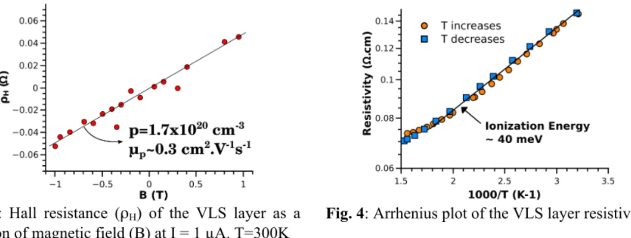
Fig. 3: Hall resistance (ρH) of the VLS layer as a
function of magnetic field (B) at I = 1 µA. T=300K
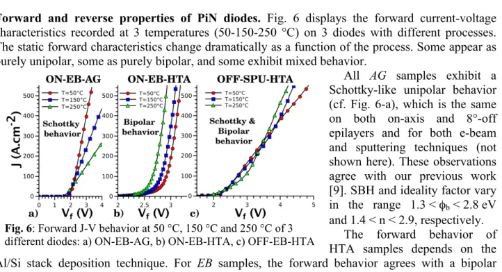
Fig. 4: Arrhenius plot of the VLS layer resistivity.
Since contacts on non-annealed samples exhibit ohmic behavior and since p-type 4H-SiC has a high work function, the origin of the ohmicity of contact is bound to originate from the high doping level of the SEG-VLS layer. This doping level has been found to be Na > 1.7×1020 cm-3 from Hall
effect measurements (Fig. 3). The extracted value of Na is in agreement with the SIMS profile of the
SEG-VLS island (not shown here). As a consequence of the very high doping level, the effective acceptor Ionization Energy is lowered to 40 meV (cf. Fig. 4) as predicted by Koizumi et al. [6]. Both the increase of the doping level and the decrease of the ionization energy favor the tunnel effect and can lead to the reduction of the SCR value at room temperature.
PiN diode with peripheral protection
In our previous work, it was demonstrated that a rather good PN junction could be achieved by using a 1 µm deep p-type SEG-VLS layer into a n--type 4H-SiC epilayer [9]. As a step forward towards the use of such localized doping process in a functional device, we report here on the
fabrication and characterization of PiN diodes using SEG-VLS process for the realization of the p+ doped emitter and guard ring peripheral protection. The influence of some key process parameters and crystal orientation on the forward and reverse electrical properties of the resulting PiN diodes will be discussed.
PiN diodes processing. Fig. 5 reports a cross section view of a typical processed PiN diode
including 3 guard rings. The area of the emitter layer is 200 x 200 µm2. Spacing between two adjacent guard-rings has been optimized by finite elements simulation on Sentaurus TCAD software. The breakdown voltage target is 1200 V. The processed samples were composed of a 15 µm thick, Nd = 5×1015 cm-3 doped n- layer grown on commercial 4H-SiC n+ wafers. Up to the VLS
growth the process steps are similar as for the ohmic contact studies. After performing the VLS growth as described in the previous section, the 500 nm SiO2 passivation layer was deposited by
PECVD. Finally, anode and cathode ohmic contacts were formed by annealing e-beam deposited metallic stacks, as described before for the anode and using Ni for the cathode.
In this paper, the influence of two main process variations has been investigated. The first one is the deposition technique for the Al/Si layers (e-beam vs sputtering), and the second one is a high temperature annealing at 1700 °C, during 30 min under Ar atmosphere, performed on some of the samples just after the VLS growth. Also, PiN diodes have been processed on both on-axis and 8°-off substrates. Table 1 exhibits the codes we have used for labeling the samples.
Table 1: Process variation and nomenclature of fabricated diodes. (For example OFF-EB-HTA is a sample made on 8°-off substrate, for which the Al/Si layers has been deposited by e-beam and the sample has been annealed at 1700 °C during 30 min under Ar atmosphere.)
Substrate orientation Al/Si deposition technique Post VLS growth annealing Variants 8°-off On-axis e-beam Sputtering 1700 °C, 30 min, Ar As grown
Sample Label OFF ON EB SPU HTA AG
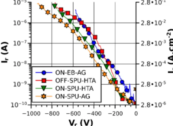
Forward and reverse properties of PiN diodes. Fig. 6 displays the forward current-voltage
characteristics recorded at 3 temperatures (50-150-250 °C) on 3 diodes with different processes. The static forward characteristics change dramatically as a function of the process. Some appear as purely unipolar, some as purely bipolar, and some exhibit mixed behavior.
All AG samples exhibit a Schottky-like unipolar behavior (cf. Fig. 6-a), which is the same on both on-axis and 8°-off epilayers and for both e-beam and sputtering techniques (not shown here). These observations agree with our previous work [9]. SBH and ideality factor vary in the range 1.3 < φb < 2.8 eV
and 1.4 < n < 2.9, respectively. The forward behavior of HTA samples depends on the Al/Si stack deposition technique. For EB samples, the forward behavior agrees with a bipolar conduction mode (cf. Fig. 6-b) while SPU samples exhibit mixed characteristics. A possible hypothesis to explain the evolution of the current conduction mode towards bipolar involves some limited diffusion of the acceptor elements during the annealing stage at high temperature.
The origin of the Schottky-like conduction is not understood yet. No intermediary phase has been detected so far around the interface zone. The only clue at present resides in the expected
Fig. 5: Cross section view of the fabricated diodes.
Fig. 6: Forward J-V behavior at 50 °C, 150 °C and 250 °C of 3 different diodes: a) ON-EB-AG, b) ON-EB-HTA, c) OFF-EB-HTA
presence of extended defects, located close to the VLS layer / n-type 4H-SiC interface, which may exhibit metallic conduction along the defects. Indeed, Sasaki et al demonstrated that Al concentration NAl > 1019 cm-3 induces a significant variation of the 4H-SiC cell parameters [10].
As a result, extended defect may be generated during the VLS growth, due to the lattice mismatch. We have made further investigations towards a better understanding of the mechanisms inducing the variations of the forward properties of the PiN diodes with VLS grown P+ emitter.
Photo-Emission Microscopy (PEM) observations have been performed on different PiN diodes in direct bias regime Id = 100 mA. The description of the MEP setup can be found elsewhere [11].
As can be seen on Fig. 7, the AG samples exhibit a low photoemission rate, which agrees with the Schottky-like I-V characteristics. For EB-HTA samples, the photoemission rate is ~1000 times higher than on AG samples and agrees with a bipolar conduction mode. Moreover, the emission is very uniform over the junction area.
In contrast the photoemission on SPU-HTA is highly inhomogeneous and the emission rate is lower than on EB-HTA samples. These additional observations confirm that the mixed “bipolar + Schottky” behavior observed on part of the samples originates from an inhomogeneous interface between the VLS p+ zone and the n-type 4H-SiC
Fig. 7: PEM pictures at I=100 mA of different processed
PiN diodes. Fig. 8: Active degradation measurements made on OFF-EB-HTA and ON-EB-HTA.
Another important issue, on the way towards the validation of a new technique for localized p+ doping, is the monitoring of the time-stability of the forward voltage Von of the PiN diodes under
direct bias operation. It is well-known that, up to know, most of the 4H-SiC PiN diodes tested so exhibit strong Von degradation due to extended defects generation and expansion [11].
Fig. 8 reports 1 hour duration active degradation measurements made on ON-EB-HTA and
OFF-EB-HTA samples at different dirrect current densities. The
“forward voltage drift” ΔVon / Von is noticeable for the OFF diodes, even at J=30 A.cm-2, while forward voltage keep constant for the ON diodes even at J=100 A.cm-2. For comparison, PiN diodes on both on-axis and 8°-off substrates, with similar geometry/epitaxial parameters and a conventional p+-type CVD layer have been characterized by some of present authors [11]. In most cases, the results were equivalent to those on the diodes with p+ emitter grown by SEG-VLS. However, on the 8°-off samples, the ΔVon / Von
was around 1 ‰ at J = 80 A.cm-2 after one hour on CVD diodes while it is more than 7 % for SEG-VLS PiN diodes at J = 80 A.cm-2.
Thus, it seems that the SEG-VLS growth on 8°-off substrate has generated a high density of basal plane dislocation which turned to Schockley Stacking Faults (SF) during forward bias operation. We have directly observed the generation and motion of SFs under forward bias on the
OFF-EB-HTA diodes by PEM imaging (not shown here). Fig. 9: Leakage current of best diode of each condition.
Fig. 9 reports the reverse I-V behavior of 4 different PiN diodes. A maximum breakdown voltage of 950 V has been measured for the ON-SPU-AG diodes, which is lower than the targeted value (Vbr = 1200 V) but strongly higher than the simulated Vbr for similar diodes without guard-rings
(Vbr < 500 V). All the measured diodes exhibit excess leakage current and the reverse voltage
measurement is limited by the SMU current compliance (10 µA). Subsequently, no avalanche phenomenon has been observed on these diodes. Therefore, we can conclude that the peripheral protection using SEG-VLS-grown p+ deep guard-rings is effective to prevent early breakdown of the junction but needs further optimization for reducing the reverse leakage current at the p+/n junction.
Conclusion
In this work, we have explored some applications of the VLS Selective Epitaxy (SEG-VLS) of highly p++ doped 4H-SiC. In a first part, we have demonstrated that good ohmic contacts could be fabricated on p-type SEG-VLS grown 4H-SiC with a SCR as low as 1.3x10⁻⁶ Ω.cm2. Moreover, the metal contacts are already ohmic on as-deposited SEG-VLS epitaxial 4H-SiC. These results pave the way towards more efficient SiC devices by replacing Al ion implantation by p-type SEG-VLS epitaxy for implementing contacts on p-type areas and the fabrication of JBS diodes.
In a second part, we have investigated on the influence of some process parameters and the substrate orientation on the properties of PiN diodes with SEG-VLS grown emitter and guard-rings. The results we have obtained demonstrate that buried SEG-VLS p-type epitaxy of 4H-SiC can be used for the fabrication of deep guard-rings peripheral protection, even if some improvement is still required concerning the quality of the interfaces.
Acknowledgment
The authors wish thank for their financial support: the Agence Nationale pour la Recherche (ANR) (VHVD-SiC / ANR-08-BLAN-0191-02), and the Swedish Energy Agency (32917-1). We would Dr. E. Bano for the access to the PEM bench. The authors would also like to thank Dr. Edwige Bano for access to the PEM bench and her kind supporting advices.
References
[1] V. Heera, C. Dubois, M. Voelskow, W. Skorupa, J. Appl. Phys. 96-5 (2004), 2841-2852 [2] K. Kawahara, J. Suda, G. Pensl and T. Kimoto, J. Appl. Phys. 108 (2010), 033706 [3] K. Ito, S. Tsukimoto and M. Murakami, Sci. Tech. Adv. Mater. 7 (2006), 496
[4] D. Carole, S. Berckmans, A.Vo Ha, M. Lazar, D. Tournier, P. Brosselard, V. Soulière, L. Auvray, G. Ferro, C. Brylinski, Mater. Sci. Forum. 717-720 (2012), 169-172
[5] D. Carole, A. Vo Ha, A. Thomas, M. Lazar, N. Thierry-Jebali, D. Tournier, F. Cauwet, V. Soulière, C. Brylinski, P. Brosselard, et al., Mater. Sci. Forum. 740 (2013), 177-180
[6] A. Koizumi, J. Suda, and T. Kimoto, J. Appl. Phys., 106 -1 (2009) 013716
[7] F. Roccaforte, A. Frazzetto, G. Greco, F. Giannazzo, P. Fiorenza, R. L. Nigro, M. Saggio, M Leszczyński, P Pristawko, and V. Raineri, Appl. Surf. Science. 258 (2012), 8324-8333
[8] N. Thierry-Jebali, A. Vo-Ha, D Carole, M. Lazar, G. Ferro, D. Planson, A. Henry, and P. Brosselard, Appl. Phys. Lett. 102 (2013) 212108
[9] N. Thierry-Jebali, M. Lazar, A. Vo-Ha, D Carole, V. Soulière, F. Laariedh, J. Hassan, A. Henry, E. Janzèn, P. Planson et al., Mater. Sci. Forum. 740 (2013), 911-914
[10] S. Sasaki, J. Suda and T. Kimoto, J. Appl. Phys. 111 (2012) 103715
[11] N. Thierry-Jebali, J. Hassan L. Lazar, D. Planson, E. Bano, A. Henry E. Janzén and P. Brosselard, App. Phys. Lett. 101 (2012) 222111