Construction and Analysis of a Real-Time Relay for Efficient
Antenna Sharing
by
Jeffrey S. Halbig
Submitted to the Department of Electrical Engineering and Computer Science in Partial Fulfillment of the Requirements for the Degree of
Master of Engineering in Electrical Engineering and Computer Science at the Massachusetts Institute of Technology
May 20, 2004
Copyright 2004 Massachusetts Institute of Technology The author hereby grants to M.I.T. permission to reproduce and
distribute publicly paper and electronic copies of this thesis and to grant others the right to do so
Author
ering and mputer Science May 20, 2004 Certified I :w Lippman ,upervisor Accepted by_ C. Smith , A"te Theses MASSACHUSETTS INSTI E OF TECHNOLOGY
Design and Construction of a Real-Time Relay for Efficient Antenna Sharing
by
Jeffrey S. Halbig May 20, 2004
In Partial Fulfillment of the Requirements for the Degree of Master of Engineering in Electrical Engineering and Computer Science
ABSTRACT
In this thesis, I present and analyze a real-time intermediate node that promotes low latency transmission of information between two endpoints. Traditional relaying via digital decoding and retransmission has inherent time delay due to limitations in
processing requirements at the transceiver, however this delay can be minimized by high speed analog amplification and forwarding rather than by processing the content of the information packets. I use a heterodyne system where the radio signal from the
originating node is translated to a new frequency band to retransmit. Latency
measurements of less than one microsecond and signal-to-noise ratio loss of 2.3 dB are found. Comparisons with a time domain multiplexing digital relaying scheme show that
analog relaying may be advantageous in applications demanding low latency.
Thesis Supervisor: Andrew Lippman
Table of Contents
Abstract... ... 2
Table of Figures
...
4
Chapter O ne:
...
51.1 Rethinking wireless communications... 5
1.2 Analog Relaying ... 6 1.3 Applications ... 9 1.4 Implem entation... 10
Chapter Tw
o:...
12
Chapter Three:
...
15
3.1 Failed Attempts... 15 3.1.1 First Prototype... 16 3.1.2 Second Prototype ... 173.2 Final Component Selection... 18
3.2.1 RF2418 LNA/Mixer... 21
3.2.3 MAX2471 Buffer Amplifier ... 22
3.2.4 RF1181B SAW Filter ... 23
3.2.5 RF2336 General Purpose Amplifier ... 24
3.3 Theory of Operation...25
3.4 Layout Considerations ... 27
3.5 Transceiver Design ... 30
3.6 Testing M ethods ... 31
3.6.1 Spectral Analysis ... 31
3.6.2 Time Domain Analysis ... 32
Chapter Four:
...
33
4.1 Relay Amplification...33
4.2 Latency Comparisons ... 35
4.3 Noise M easurements... 39
4.4 Power and Size Characteristics... 41
Chapter
Five:...
42
5.1 Power and Size Issues... 42
5.2 Noise Performance...43
5.3 Real-Tim e Operation ... 44
5.4 Future W ork... 45
5.5 Conclusions... 46
Table of Figures
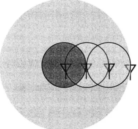
Figure 1: Relaying reduces total energy by 1/#hops... 7
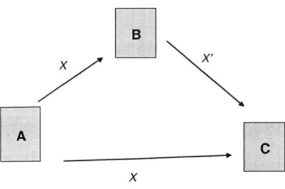
Figure 2: Diversity scheme employing a relay (B) to redirect a signal (X) from a transmitter (A) to a receiver (C). Two such systems are described by Laneman.... 13
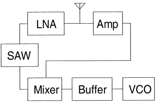
Figure 3: Simplified analog relay block diagram. ... 19
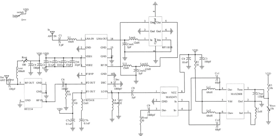
Figure 4: Analog Relay Schem atic ... 20
Figure 5: Printed circuit board layout ... 28
Figure 6: Spectrum analysis showing relay frequency conversion and signal amplification. Plot taken for input signal of -5 dBm. Received signals are at -38 dBm and -49 dBm for 433.92 MHz and 916.5 MHz signals respectively... 34
Figure 7: Chart of transmitted power vs. relayed and direct received power... 34
Figure 8: Packet transmission through relay showing simultaneous transmission and recep tion ... 36
Figure 9: Delay through relay from transmitter TX pin to receiver RSSI pin... 36
Figure 10: Delay without relay from transmitter TX pin to receiver RSSI pin... 37
Figure 11: Received digital packet showing 3.48 ms separation... 38
Figure 12: Reception of direct and digitally relayed data showing packet length delay.. 38
Figure 13: Analog relayed signal and transmitted signal at baseband with noise... 40 Figure 14: Digital reception without relay and associated transmitted signal at baseband.
Chapter One:
Introduction
1.1 Rethinking wireless communications
Wireless is becoming the preferred mode for many types of communications. Not only does it provide easy mobility, but it also adds flexibility to stationary systems. Cell phones, PDAs, and portable computers are examples of the former. Cordless telephones and home wireless networks are examples of the latter. It is simpler to install a wireless Internet port than to rewire a house for each new hookup. A problem with these systems is the difficulty in scaling them. Cellular telephony, for example, operates by connecting each individual phone to a tower. If there are too many phones in use in one cell, it
simply fails to connect new calls or accept existing calls that roam into the cell. In order to allow technology to scale with the large growth of wireless communications to come, current architectures for wireless networks must be rethought.
Wireless networks are defined by a collection of nodes in which one or more connections are made through radio transmission of information. In particular, the implementation of an ad hoc network potentially solves some of the scalability issues. An ad hoc network consists of several nodes all communicating wirelessly without any centralized control or previously established infrastructure [2]. Each node in these networks serves as a
destination for transmitted signals while also serving to relay received transmissions to their intended recipients. This is optimal for increased mobility and flexibility as the network can be constructed and torn down in very short time, and, due to the multi-hop nature of transmitting information, communication can happen between nodes far out of direct range from each other while transmitting with only enough power to reach its closest neighbor [4]. The small broadcast power frees space that would otherwise be saturated with the transmitted energy and allows spectrum reuse. In such a way one can increase the information capacity of a given area.
An ad hoc network that displays such behavior could be called viral. The general theme of a viral network is to exhibit three key parameters. First, it should be de-centralized so that the intelligence is distributed at the end user. Second, it should scale to allow
virtually unlimited use and access. Lastly, each additional member of the network should increase the network's net utility. The traditional client-user relationship in today's communication standards is greatly limited by not allowing its users to take advantage of the resources of each network member. A viral network looks to change this relationship so that by sharing the abilities of neighboring users, the bounds of current architectures can be far surpassed.
1.2 Analog Relaying
The fundamental issue in this thesis is to explore an efficient way for a viral network to transfer information to and through its neighbors. Analog relays offer an opportunity to
reduce the necessary transmission energy required to get the same end-to-end signal-to-noise ratio (SNR) as in the direct transmission case. The amount of energy needed is less than 1 / k2 energy per hop, or less than 1 / k of the energy in total for a system of k-1 relays and one receiver. This concept is displayed in Figure 1. The ability to exploit idle users in a viral network as analog relays thus creates more efficient signal propagation while freeing space for other communication paths.
Figure 1: Relaying reduces total energy by 1/#hops
The largest concern when planning an analog relay implementation is the necessary addition of energy to each relayed signal and minimizing the retransmission latency. The core problem is the construction of a real-time, amplifying relay. Both issues are
immediately addressed by using an analog scheme rather than a digital one. Traditional relaying via digital decoding and retransmission has inherent time delay due to
limitations in processing requirements at the transceiver, however this delay can be minimized by high speed analog amplification and forwarding rather than by processing
the information content. All that is needed is a high-speed amplifier coupled with a reception device to receive and retransmit on a separate channel.
It is not possible to transmit at the same time one is receiving through the same antenna at the wavelengths of interest. Therefore, the solution has to involve some form of
multiplexing. One could alternate reception and transmission times (TDM), with little delay. In this thesis, I have used frequency domain multiplexing. The relay receives on one frequency and transmits on another. This allows simultaneous transmission and reception at the expense of using two channels for a single data path. The end node receives on both channels and makes a best guess at the data. The advantage of this scheme is that more intermediate nodes can be used, thus building up at the receiver a set of relayed information replicas from a number of transmitters on each channel. In this fashion, only two channels are needed independent of the number of hops. This would be more complicated with a TDM structure.
Although an analog repeater seems to assume continuous reception and transmission, in a real system, each potential intermediate node still has to make some decision about whether it will re-transmit the information, or else the space will become overloaded with spurious broadcasts. In this thesis, I do not address the problem in detail. It is sufficient for the work done here that when the motion of the nodes is slow compared to the packet rate, an intermediate node can make the relay decision once and maintains state for the
remainder of the transmissions. It is also true that the decision to continue to relay can be made in parallel with analog retransmission and expire when the conditions so warrant.
1.3 Applications
Large-scale wireless networks where multiple relay hops are utilized for a
communication path would benefit most from such a scheme. In a multi-hop scenario, any minimum delay threshold is reached quite rapidly when each intermediate node has to analyze the packet to make a routing decision. Since each digital relay must accept a
full frame, decode, and retransmit the frame, the incurring delay is equal to the time it takes to fully accept the transmitted packet plus the processing time to decode, re-encode, and retransmit. For some current relays used in the Media Laboratory, this is on the order of 1.7 milliseconds for a 32-bit packet. The analog relay presented in this thesis has a latency of less than 1 microsecond. If a communication over a certain distance requires less than a millisecond of delay between transmission and reception, only one digital relay at a given power can be utilized to aid in this transmission. Several analog relays can achieve the same transmission under the latency threshold and less total transmission power since each transmission has a shorter propagation path. Any system transmitting fast time-varying signals, such as in position tracking, or two-way voice communication, is sensitive to delay and could benefit from a low latency relay. The limitations of this system come from the additive noise at each analog node, as well as the added bandwidth required to operate on multiple frequency channels.
Radio propagation is different from normal network routing. In the latter, a usually unique path is defined between the sender and receiver of information. Ad hoc network research has converged on four such algorithms where the routing intelligence is
distributed among the nodes and changes with the geometry and accessibility of nodes. However, any individual packet is usually sent over one path.
In radio networks, more than one node may relay the information, and the ultimate
recipient can receive signal energy from more than one emitter. It has been shown that as long as the multiple sources are independent and uncorrelated, each individual
transmission can add to the reliability of the end-to-end communication [1]. In essence, this thesis is a realization of that theory. I emphasize the potential for networks that use this notion of "flux propagation" through an analog relay, rather than routing, for signal distribution.
1.4 Implementation
An analog amplifying relay is constructed and characterized for use in a viral antenna sharing scheme. The general form of frequency domain multiplexing used is a heterodyne system where the incoming 916.5 MHz signal is mixed down to an
intermediate frequency of 433.92 MHz. A linear amplifier adds energy into the signal and retransmits at varying gains. Extensive detail in the method and process of
engineering the relay is documented throughout chapter three, including component selection and board layout.
Signals used to study the latency, error rates, and SNR of the relay are generated by prototype 916.5 MHz radios used extensively in the Viral Communications group at the MIT Media Laboratory. These same transceivers are also used for signal reception. Further detail on these boards is also documented in chapter three.
Chapter Two:
Background on Previous Research
The original aspect of the thesis is that no known previous research has been done to study a realization of analog relays for ad hoc networks. The idea of antenna sharing through analog relays has been thoroughly documented however. The bulk of this thesis idea stems from the work of J.N. Laneman and G.W. Womell at the Research Laboratory of Electronics at the Massachusetts Institute of Technology. The paper cited [1] performs mathematical analysis on a three-node multi-hop scheme based on energy transmission and probabilistic detection equations. Specifically, an analysis of single-hop
transmissions is compared with two relaying schemes. Figure 2 shows the configuration of the relaying schemes discussed. The first scheme allows for the relay to decode the incoming signal, estimate its value, and retransmit to the receiver; the second is the amplifying and forwarding model that is the inspiration for my work. The conclusion of their paper is that although there are benefits to both relaying methods, namely that the additional energy supplied by the relay gives gains in either reliability or transmission power. However, analog amplification provides optimal results despite additive noise at the receiver [1], mostly due to the chance for error propagation from the digital relay. For this reason, my relay applies purely analog amplification.
x'
A
C X
Figure 2: Diversity scheme employing a relay (B) to redirect a signal (X) from a transmitter (A) to a receiver (C). Two such systems are described by Laneman.
Others who have done similar research include Zahinoglu and Orlik who compare digital and analog relays in the multi-hop scenario without diversity combining. Their
conclusion is that their benefits are nearly equal with the slight edge given to analog for less processing power consumption [5]. Zheng has described the benefits of adding relay nodes to improve channel capacity or energy conservation [6], and still others have explored optimum transmission ranges and the efficiency limits of multihop ad hoc networks [7].
A. Bletsas and A. Lippman have published work detailing the use of a system similar to
that described by Laneman based on orthogonal time slots rather than frequencies. Their paper [3] utilizes OFDM on identical channels between relay and transmitter to the destination while gaining energy and error-rate efficiency thus increasing network
capacity. Their theoretical models parallel that of [1] and serve to support construction of such a system. A. Bletsas followed this with work on a power management scheme that
demonstrated increases in capacity for a given space on one channel through transmission via relay. This work was constructed and demonstrated at the MIT Media Laboratory in October 2000. The content of this thesis complements that of others in the Viral
Communications group at the Media Laboratory as well as that of those previously mentioned.
Chapter Three:
Method of Relay Design and Testing
The fundamental issue addressed in this thesis is the construction and characterization of a real-time analog amplifying relay. The design is entirely board level, with the
necessary building block circuits supplied from chip manufacturers. By properly
selecting the correct components and engineering their interface with each other, a basic prototype for analog relays that may be incorporated into future wireless viral networks is created. The evolution of the device progressed through two failed prototypes and
several measurements to ensure that the third and final version functioned correctly, particularly within the requirements of the relay device in a viral networking scheme.
3.1 Failed Attempts
As with most projects in engineering, mistakes must be made in order to make progress toward the final goal. This project was no exception, there were two analog relay
prototypes developed before completion of the third and final version. The difficulties in engineering a piece of high frequency electronics lie largely in capturing and transferring energy throughout the board. Careful attention needs to be placed when selecting the
appropriate components for signal processing as well. Just because a chip performs the desired function in theory, it may not do so when interfaced with other parts of the circuit or may only do so after solving difficult matching problems.
3.1.1 First Prototype
The first version aimed to achieve amplification and frequency translation from 916.5 MHz to the commonly used 868 MHz band. It largely failed for all of the previously mentioned reasons, as well as for easily avoidable layout mistakes. The design was kept too simple and a number of unseen issues were not addressed. The board consisted only of the Tachyonics TARF2304 double-balanced mixer for frequency conversion, a 48.5 MHz oscillator used to provide the difference frequency to the mixer, and a surface acoustic wave (SAW) bandpass filter for image rejection at the input. It was assumed that the minimum mixer conversion gain of 10 dB would be sufficient for amplification, that the 50 ohm components would match each other and provide ideal power transfer without external considerations, and that the loop from input to output would be stable.
Not only were all of these assumptions incorrect, but also the chosen oscillator was not at all compatible within the input power requirements of the mixer. Also detrimental were some incorrectly designed component footprints on the printed circuit board (PCB). It was necessary to hand wire some circuit pins to each other to properly assemble the circuit because of these incorrect footprints. The end result was a board that showed almost no functionality. Probing of the board with a spectrum analyzer and signal
generator, as well as reading the data sheets of each component more carefully, led me to believe that I needed two important changes to the topology. First, an output driver was required to further amplify the incoming signal through the output antenna, and second, a
to the mixer should replace the more clock-like oscillator chosen for the first version. I also noted to take more care in my PCB layout and to look deeper into the details of each component datasheet before assuming compatibility between circuit chips.
3.1.2 Second Prototype
The second prototype shifted gears slightly and aimed to amplify the signal onto a 433.92 MHz output rather than 868 MHz, mostly due to the ready availability of 433.92 MHz components. Different from the previous version was a change in oscillator to the
MAX2608 VCO, a VCO specifically tailored to serve as a local oscillator for RF mixers.
Its -10 dBm of output power was compatible with the necessary input power to the TARF2304 [11]. Also added was the AD8353, an RF power amplifier to drive the output to the antenna. It served as a fixed gain block of +20 dB to add upon the 11 dB gain of the mixer [15]. This version also included a middle layer ground plane in the PCB rather than rely on the negative battery terminal for a voltage reference. This is a key
component to limiting undesirable noise, ground loops, and low antenna gains.
Again, power transfer was a large problem and led to the relay failing. The board showed functionality when probed directly at its output but was not transferring enough power to the antenna to transmit a detectable signal. There was also a large amount of spurious frequency noise that seemed to come from feedback within the loop. I concluded that since the board was down mixing the incoming frequency, the mixer and VCO were operating correctly but the amplification was attenuated by incorrect impedance matching
and SAW filter insertion loss. I also decided that having two separate input and output antennas would help to prevent any strong feedback of the signal through the board and reduce spurious noise. Further research into the interactions between the PCB substrate
and the board traces showed that it was necessary to precisely engineer the size of the PCB traces and thickness of the substrate to create a matched 50 ohm transmission line for maximum power transfer through the circuit.
3.2 Final Component Selection
To fully understand the design behind the functional relay prototype, one must look into each individual component and how it adds to the overall system. After having learned from the previous failed prototypes, I chose a clear block diagram as displayed in Figure
3 for the general topology. The detailed schematic is displayed in Figure 4. The layout
mimics a combination of the front-end of a receiver and output stage of a transmitter. The same topology is used in the transceivers of many consumer products such as mobile
phones making high-quality components readily available. The design is not without flaws, but improvements should come from additions to the topology rather than corrections to faulty circuit implementation. All components achieve their desired functionality, yet the level of performance is overestimated in some instances.
LNA
Amp-SAW
F Mixer
oBuffer
VCO
\'DD
0-Outi
In G od G d' 6
I
1 LNAIN LNA OUf 14 Lrnclt 1 h-fti
5 pF Crncliln tU3
Ilikz_ ND GND 3 T~pFRFl 181B D
Rout 'VL)) D VDD 2
Lot 1001f tu
Ou I~l IF BYP GNDI101 p Col O
Ntv 'ut '0 5 F T TN 1
0p
ANT p C6 1 de
ol Out- Tunte 3R10
GNI{.{ 8uHMAX2608 Chyp
I 20p I 4GM) InI Vdd Gd2 ---- Rtunu RF234VI4: Lf 10k - IOut+ hid
3.2.1 RF2418 LNA/Mixer
The RF2418 by RF Microdevices Inc. is an integrated UHF receiver front end with a specified frequency input range of 1100 MHz to 400 MHz, ideal for reception and translation from 916.5 MHz to 433.92 MHz. The main attraction of this chip is the numerous blocks it incorporates onto one monolithic chip. A combination of low noise amplifier (LNA), RF amplifier, double-balanced mixer, and output buffer greatly simplifies the design of the input and down-converting stage of the relay. The only necessary components to surround the chip with to complete the front-end of the board design are a voltage controlled oscillator (VCO) serving as the input for down
conversion, and a SAW filter to filter spurious frequency noise from the data path. The required supply voltage range is from 3V to 6.5V and draws 60 mW of power while operating, qualities that make it easily powered by three AA batteries. Total gain through the three amplifying sections (LNA, RF amp, and mixer) is a typical 47 dB and the noise figure totals 14.2 dB giving a SNR gain of almost 33 dB. The internal impedance
matching and low impedance output are also of note since power transfer is the biggest concern in the design. These qualities simplify the overall design by eliminating the need for matching several components by optimally integrating them onto one chip. The only downfall of the RF2418 is the high level of oscillator power required from the VCO for proper operation. This led to the addition of a VCO buffer that would have been unnecessary for some other mixers [10].
3.2.2
MAX2608 Voltage Controlled Oscillator
This voltage controlled oscillator is the same component used in the second prototype. I was quite happy with the behavior of the VCO in the last revision and decided to
continue with what works. Many characteristics make it a desirable VCO for use.
Physically, the 6-pin SOT-23 package it comes in is a common PCB footprint for ease of layout design, and it is also very small at nine square millimeters. From a circuit
perspective, it is able to run from a 4.5V supply while draining a small 12 mW of power. Perhaps most important is that it features phase noise of -100 dBc/Hz. It is crucial that all components be low in noise as this is the limiting factor in the effectiveness of analog relays in a viral network. An added feature of the MAX2608 is the wide tuning range. A
signal from 300 to 500 MHz is generated from the adjustment of only an external inductor [11]. External resistors are added to allow for fine-tuning of the DC voltage input to the VCO for exact mixer translation to 433.92 MHz.
3.2.3 MAX2471 Buffer Amplifier
Unfortunately, the -10 dBm output power from the MAX2608 that was compatible with the TARF2304 is not strong enough to drive the RF2418 mixer. The MAX2471 is a compatible buffer amplifier for use in conjunction with the MAX2608 to isolate the VCO
from remaining circuitry and provide gain to the oscillator signal. It also serves to convert the VCO differential output to the single-ended output required by the mixer. Characteristics of the buffer include a supply voltage range of 2.7V to 5.5V and power
consumption of 25mW, an input frequency range of 10 to 500 MHz, and the same small
SOT-23 package as the MAX2608. Output power for an input of 482.58 MHz at -10
dBm approximately -2 dBm, easily increasing the power of the VCO beyond the required
-6 dBm mixer input level. Another benefit of this particular buffer is the -29 dBc
harmonic suppression. Any stray harmonics that enter the mixer lead to spurious noise at its output caused by the multiplication of the input signal with these undesired
frequencies. The low 8.4 dB noise figure is also advantageous to the overall circuit design [12]. In summary, the combination of the MAX2471 and MAX2608 makes for a quality, low-noise, adjustable reference for mixer down-conversion.
3.2.4 RF1181B SAW Filter
The RF1181B is a bandpass SAW filter specifically engineered to pass 916.5 MHz signals. Though this component is withdrawn from the final relay implementation, it would be a necessary component in a more powerful relay for noise rejection. It attains a maximum out of band rejection of 80 dB with a minimum rejection of 20 dB from 10 MHz around the filter frequency. These characteristics are great for filtering any unwanted signals such as noise, pickup, and harmonics. However, the gain comes at a large cost. A four dB insertion loss is inherent in the SAW filter, which is counter productive to attaining maximum power transfer through the circuit. Also of concern is the 500 ns delay in signal propagation [13]. Fortunately, the relay circuit does not suffer from dramatic noise problems and this component can be bypassed to achieve maximum speed and power, yet it should be considered when low noise is of highest priority. If the
SAW device is used, it should be accompanied with another power amplifier to counter the insertion loss.
3.2.5
RF2336 General Purpose Amplifier
The final component selected to complete the fundamental blocks of the analog relay was the RF2336 power amplifier. Rather than depend on a general gain block like the
AD8353, this component is specifically tailored as an output amplifier for a low power
radio system. The DC to 6 GHz operating frequency range, SOT-5 package, impedance matched input and output, and greater than 4.3V supply voltage all make this a desirable component superficially. The greatest specifications are its output power and noise figure. The linear output power is specified at 10 mW, or 10 dBm, and a typical small
signal gain of 20 dB for operation at 433.92 MHz. Output power of 10 mW is expected to be sufficient for several meters of broadcast range and is satisfactory for the testing purposes of the analog relay. The noise figure is quoted at a very low 3.8 dB, further limiting the added noise in the circuit and maintaining high signal SNR. One particular drawback to the chip is the nature of its output. An external pull-up resistor and inductor
are required to correctly bias the output transistor of the RF2336, giving unprotected access to a power sensitive section of the circuit. On several occasions the chip needed to be replaced on the relay prototypes because careless adjustments were made that supplied
greater than the 48 milliamp maximum input [14]. In general though, the amplifier is simple and effective for driving an antenna output.
3.3 Theory of Operation
The basic premise of the relay is to utilize the frequency differencing properties of an analog multiplier to transfer an incoming data signal onto a non-interfering, or
orthogonal, frequency. The second requirement is to add energy to the signal as it
propagates; therefore amplifiers are also a key component in the design. Each component selected adds necessary function to the behavior of the relay. The details of the
components mentioned can be found in section 3.2.
The first element encountered by an incoming signal is the antenna. The frequency of interest is 916.5 MHz, which corresponds to a wavelength of 32.73 cm following the equation A = c/ f . A quarter-wave style antenna is used for simplicity, and a copper wire
trimmed to 8.2 cm serves this purpose. This passes to a series resonant LC circuit that acts to transfer the power of the 916.5 MHz signal into the LNA of the mixer. The LC resonance is at f = 1/ 2rc , and following the recommended 10 nH inductor value for the RF2418, the capacitor is set at 5 pF, the closest available value to the exact 3 pF for resonance.
The signal then proceeds to the RF2418 LNA/Mixer module. First, the signal is
amplified with a gain of 14 dB by the LNA. The external SAW filter stage that follows the LNA output is bypassed to avoid the inherent signal attenuation and delay associated with SAW devices, and the signal is again amplified by the internal RF amplifier for
mixing with the VCO frequency. Down-conversion at the mixer is achieved by taking advantage of the multiplication-convolution relationship between time and frequency responses.
x(t)-y(t)= X(f )*Y(f)
The multiplication of two time varying signals, in this case a data stream modulated onto a high frequency carrier and a fixed frequency oscillation, directly corresponds to the convolution of their respective frequencies. In this application the convolution of the
frequencies 916.5 MHz and 482.58MHz produces replicas of the 916.5 MHz signal at the sum and difference of the two frequencies giving a down-converted signal at the desired 433.92 MHz as well as an undesired signal at 1399.08 MHz. This high frequency component is not of interest and its effects on transmission are ignored.
The reference frequency for mixing is supplied by a buffered VCO. The VCO is tuned to
482.58 MHz via an adjustable voltage divider from the power supply and an external
tuning inductor of 12 nH. The supply is thoroughly bypassed so it is assumed that variations are minimal enough to consider the tuned frequency as constant and in practice this seems to be the case. The output frequency reference is taken differentially into the buffer amplifier. The buffer amplifier raises the power of the oscillator signal to -2 dBm in accordance with the input requirements of the mixer. To get this single-ended input from the differential input, the negative end of the signal is terminated in an appropriate
through a series capacitor-shunt inductor filter with values recommended by the manufacturer.
The down-converted signal from the mixer is buffered by the internal components of the RF 2418 for 50 ohm impedance matching. The external passive network present at pin seven of the mixer serves to bias this output buffer. The signal is then AC coupled to the RF2336 power amplifier for transmission. The output stage of this amplifier is biased via the external 100 nH inductor and 30 ohm resistor and provides a gain of 20 dB, or
maximum output power of 10 dBm. The amplifier drives the AC coupled antenna, sized to a 433.92 MHz quarter-wave length of 17.3 cm. Broadcast of unwanted signals such as components of the frequency convolution are attenuated at the output by the filtering characteristics of the 433.92 MHz quarter-wave output antenna.
3.4 Layout Considerations
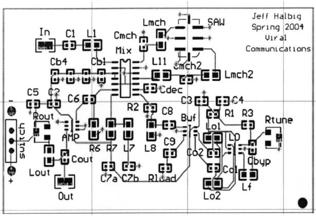
A schematic of the board layout can be seen in Figure 5. All traces are located on the top
layer of the board and a ground plane is located in the middle layer that is accessed through vias. The printed circuit board was designed using the 99 Protel SE software
CAD package. Each component footprint was carefully designed to meet the size
specifications outlined in their respective datasheets with the exception of the passive elements that are used in standard 0603 and 0805 footprint dimensions. Beyond the generic placement of components and design of their footprints is an incredibly important
aspect of engineering the analog relay. When working at frequencies in the high
hundreds of megahertz, it is essential that great care be taken in the layout of the circuit.
Lmch
-
SA
J fn
i
ilCnch
Sprin..12004[l
Cmh
Viral
Mix 1.
Jl!
.iix Communciat ionsCb4
L
AM-
L11
Cn
h
Lmch2
C5
'-B
dec
& + ot
R2
CS
P 1 P3
ou
U'1f
Rtu,e
LOut
+v]j 7-401
D
Lo2
.
Figure 5: Printed circuit board layout
It is very important that a solid ground plane be established on the PCB. This serves as the reference voltage point for the entire circuit as well as a limiter to capacitive coupling within elements on the board. Each pad has a small amount of capacitive coupling between it and each other element on the board, but if there is a large ground layer below all components then there exists a large capacitive element to ground in proximity. It also serves as a controlled path for return currents that keeps signals localized on the board [8]. The middle layer of the board examined is a ground layer made of 1 oz. copper and is accessed from the top component layer by vias, or through holes on the
board. The ground plane also serves as a near field reflection point for the antennae that enhances its gain and directionality. The depth of this plane is also a large factor in determining the characteristic impedance of the PCB traces that interconnect each component, and thus instrumental in how effectively power is transferred in the circuit.
The PCB traces combined with the ground plane beneath it form a transmission line with a particular characteristic impedance. In order to get maximum power transfer from a transmission line, all impedances the signal encounters must be equal or else reflections
occur on the line that cause attenuation. This impedance is a function of the trace thickness (T), trace width (W), dielectric constant of the board material (er), and the height of the board separating the trace from the ground plane (H) as shown in the equation below [9].
87 in_5.98H_)ohms
E, + 1.41 0. 8W + T
The FR4 material used for the PCB has a dielectric constant of 4.1, a trace thickness of
1.35 mils, and a trace width of 10 mils. These parameters make it necessary to place the
top layer traces exactly 6.026 mils above the ground plane for the desired 50 ohm characteristic impedance.
To limit the effects of the signal feeding through to unwanted parts of the board, it is necessary to separate the input, output, and VCO sections of the circuit as much as possible. Placing the input and output antennas at the extremes of the top and bottom of
the board helps prevent the output or input from leaking through to each other and causing interference. The high power VCO signal is placed even further away at the far right of the board to isolate it from all other parts of the circuit. Another technique to limit unwanted signals from the signal path and limit parasitic effects is to keep signal traces and component leads as short as possible [9]. All ground plane connections on the board are made immediately next to the pad on which the component is soldered and almost every ground connection is given its own via to reduce the parasitic inductance present on them. Reduction of power supply noise is achieved by bypassing frequently at each power supply connection. Ceramic capacitors of values varying from 22 pF to 1 uF are scattered throughout the supply connections to assure filtering of a wide range of unwanted frequencies. These leads are also kept as short as possible to limit the effects of parasitics.
3.5
Transceiver Design
To conduct tests on the performance of the analog relay, it was necessary to have source and destination radios. Aggelos Bletsas and Josh Lifton of the MIT Media Laboratory designed the prototypes used. The structure of these transceivers is very simple. A quarter-wave antenna is attached to the printed circuit board and wired to one of either of the RFM DR3000-1 or DR3100-1 transceiver modules, for 916.5 MHz and 433.92 MHz operation respectively. Control for the module is handled by the Chipcon C8051
transmit or receive mode. Two AA batteries power these radios. The RFM modules have received signal strength indicator (RSSI) pins for power and noise measurements as well as easy access to the RX and TX receive and transmit pins for access to the
baseband data received or transmitted. Performance of these modules may be limited due to the absence of a ground plane in the board layout.
3.6 Testing Methods
Both spectral and time analyses were performed to characterize the behavior of the analog relay. Spectral analysis shows the transmitted frequency bands as well as their relative signal strengths. The time domain analysis allows examination of signal to noise
ratio and respective latencies for both digital and analog relaying.
3.6.1 Spectral Analysis
Gain and frequency characteristics were measured using the Agilent E4403B 3GHz spectrum analyzer and E4421B 3GHz signal generator. For the measurements, the relay was situated between the two instruments at a distance of 6 inches from the antennas of each. A 916.5 MHz signal was generated by the E4421B at powers ranging from 10 to
-30 dBm at 5 dBm intervals. Both direct and relayed signals were then inspected at the spectrum analyzer. The corresponding input levels were recorded for both signals and are compared in chapter four. The spectrum analyzer was also used to tune the output frequency of the relay to precisely 433.92 MHz.
3.6.2 Time Domain Analysis
The latency and signal-to-noise ratio characteristics were measured using the Agilent 54622D 100MHz oscilloscope. The transmitter and receiver were each placed 6 inches apart from the relay on either side in a linear fashion. Data sent was measured at the RSSI pin of the transceiver module to study reception characteristics, and the data transmitted was probed at the TX pin. Measurements of analog and digital relayed data, and directly transmitted data were taken. All measurements were of the demodulated baseband signal found at data pins on the transceiver. In the case of the digital latency measurement, where the transmitted and relayed signals are at the same frequency, testing consisted of taking separate plots of reception with and without the relay active. The testing environment was indoor and non-dynamic. Results of these tests can be found in chapter four.
Chapter Four:
Results
Signal-to-noise ratio, gain, and latency are the key parameters to analyze for a sound characterization of the analog relay and determination of its use in a viral network scheme. The following plots and charts reflect the capabilities and shortcomings of the final design. Interpretation of the significance of each measurement is discussed in chapter five. The method carried out for each test is described in chapter three.
4.1 Relay Amplification
One of the most important aspects of the relay is to add energy to the retransmitted signal so that fading effects of the overall transmission are attenuated. It is also necessary for the receiver to get the added benefit of more information to make a reliable decision on the value of the data. A spectrum analyzer plot showing the gain and down-conversion of the signal through the relay is shown in Figure 6. An accompanying graph of the measured gain characteristics over the tested broadcast power range is displayed in Figure 7.
Figure 6: Spectrum analysis showing relay frequency conversion and signal amplification. Plot taken for input signal of -5 dBm. Received signals are at -38 dBm and -49 dBm for 433.92 MHz and 916.5
MHz signals respectively.
-70
-80
Transmitted Power (dBm)
Figure 7: Chart of transmitted power vs. relayed and direct received power
10 5 0 -5 -10 -15 -20 -25 -30
-- 916.5 MHz Received Power
-I- 433.92 MHz Received Power
0 -10 -20 -30 -40 -60 0 0 a. 0 0 0
Figure 6 shows the effective down-conversion from 916.5 MHz to 433.92 MHz clearly. Also of note in the spectral analysis plot is the lack of any serious spurious signal noise.
A small lump in the spectrum around the VCO frequency of 482.58 MHz is apparent, but
well attenuated below the signal levels.
Figure 7 shows a close to linear gain of between 9 and 11 dB between inputs of -5 and -30 dBm and an expected monotonic decreasing trend as the input power is decreased. The non-linear behavior at the high input levels may be due to saturating effects in the amplifiers of the board.
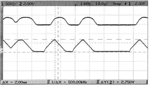
4.2 Latency Comparisons
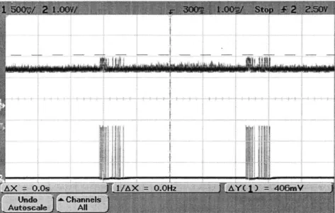
One of the requirements for the analog relay is that it operates in real-time. In other words, the delay, or latency, of the signal processing through the board toward the receiver should be as minimal as possible. The characteristic of small latency is one of the advantages of an analog relay over its digital counterpart. Time domain plots are shown below in figures 8 through 10. The plots can be used to make direct comparison between the digital and analog relaying schemes.
Figure 8: Packet transmission through relay showing simultaneous transmission and reception.
X 2.1OAs f /IIX = 500.0 kHz AYC = 406mV
...
-AX ~___ I/x _____s 500nH--z-
-
.70-I(2
Figure 10: Delay without relay from transmitter TX pin to receiver RSSI pin.
Upon inspection, an approximated 2 gs latency is observed between transmission of data from baseband at the transmitter and the baseband reception at the receiver. It is hard to quantify the exact delay of the analog relay because there is no exact point where the transmission could be deemed transmitted or received. The two response times seem to be identical on the 1 pis level. Though precise quantification of the delay is not possible, an estimate of less than a microsecond of latency through the analog relay is reasonable. The remainder of the latency can be attributed to the signal propagation through the transceiver module.
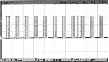
As a basis for comparison, plots of the reception with and without digital relaying are displayed in figures 11 and 12. The inherent delay of this digital relaying scheme requires a time scale on the order of a packet length. Since the relayed signal uses
identical frequencies, both relayed and direct transmissions are captured on altering time slots.
A1X 3.466ms _) ' U 1AX =28 7.3 6Hz j AYC 4)1 O.OV Figure 11: Received digital packet showing 3.48 ms separation.
F X =1.760ms AX 568R1ed relaYyed dat showin p acke lnt delay.
Figure 12: Reception of direct and digitally relayed data showing packet length delay.
The latency of such a digital system is equal to the time it takes to transmit an entire packet of information; in this case the packet length corresponds to 1.76 ms. Figure 11 shows transmission without a relay. The large gaps correspond to silent periods maintained for relayed transmission. Figure 12 shows the utilization of these gaps and the large inherent delay in such a scheme.
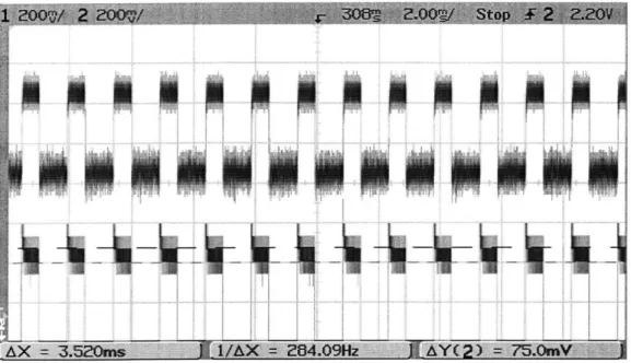
4.3 Noise Measurements
It is largely acknowledged that the noise added by an analog relay is the limiting factor for its usefulness in an ad hoc network [1]. Specifically, the signal to noise ratio cannot exceed the sensitivity of the receiver, or else the data will be highly unreliable. Though it has been shown that a digital relaying scheme has large latency deficiencies, it has the benefit of noise immunity through signal regeneration. Figures 13 and 14 give direct comparison of the noise levels present in both the digital and analog transmission cases.
WAIt-AX 3.520 11/AW 2d4 l9H jf Ya 7.m& 'H
Figure 13: Analog relayed signal and transmitted signal at baseband with noise.
a wO
r
AX= 3.520mvs 1/AX 204.0914z. z. Y3pry
Figure 13 shows the analog relayed baseband signal as the top waveform and the crest of the baseband transmitted signal. The analog relay shows 100 mV of peak-to-peak noise
as the black portion at the top of the signal. The transmitted signal is measured to have
75 mV of noise. Figure 14 is an identical plot without the intermediate relay. The noise on the baseband is now reduced by 30 mV. The SNR is determined as the peak-to-peak signal divided by the peak-to-peak noise; in this case, the SNR is approximated at
500m V / I00mV =5 for the analog relayed signal, and 450m V / 68.8mV = 6.54 without the
relay. This corresponds to a decrease in SNR of 2.3 dB when propagated through the analog relay.
4.4 Power and Size Characteristics
The board is sized at 8.2 cm x 4.8 cm square, and the power consumption is specified at approximately 284 mW.
Chapter Five:
Practical Functionality of the Relay
The gathered information on the gain, latency, and noise characteristics of the analog relay leads to a discussion of how practical such a device would be in a viral networking scheme. There are some obvious discrepancies between the digital and analog relaying schemes, such as the differences in latency, and some that may need further insight for the proper conclusions to be drawn, such as noise considerations. Each is worth some discussion.
5.1 Power and Size Issues
It seems counter-intuitive that an element that is consuming 284 mW of power is a benefit to the energy expenses of a wireless network. The truth is that even though there are savings in the total transmitted power, a unit that stood alone as a relay and consumed 284 mW of power would be undesirable. A similar argument goes for the size of the device. A block of 39 square centimeters would not be a welcome addition on any practical device, particularly a mobile one. Fortunately, the design of this particular frequency domain multiplexing relay only uses components already used in current wireless products. For the small cost of bypassing the digital circuitry when in relay mode, the same basic relay could be implemented on a mobile phone or wireless Internet
card. The energy consumed would be on the order of the amount of energy consumed while the device is active in normal transmit or receive mode, and there would be little added size. Though the added drain of relaying on the system would still lead to shorter battery life, the incentive to relay and be relayed for seems a worthwhile tradeoff.
5.2
Noise Performance
The added noise in the system by adding the analog relay is quantified to be approximately 2.3 dB. This is an extremely promising figure, especially when
considering that by incorporating the SAW filter back into the functional unit one could reduce the noise even further. A simulated viral system presented by Laneman displays
analog relaying gains with diversity combining at the receiver to be as much as a factor of
15 dB in SNR [1]. Even though the tested system is not gain controlled as is assumed in
the reference, all 2.3 dB of noise could be added onto the simulated system, as a worst case scenario, and still show gains in SNR efficiency well above 10 dB. However,
analog relaying is shown to be only slightly advantageous over intelligent digital
relaying. The added noise may take this slight advantage away from the analog case, but since the only assumption in the simulations is that the SNR is large, no conclusions can be drawn.
The error probability tolerance of a system sets the number of analog relays that could be used in a multi-hop scheme. Each added hop decreases the total SNR in a non-diversity combining scheme by 2.3dB, and thus decreases the reliability of the detection.
Unfortunately, data on such a system could not be collected due to malfunctions at the RX pin on the 433.92 MHz transceiver module. This would be a very interesting experiment to conduct, and should be followed up in future work.
5.3
Real-Time Operation
The goal of real-time operation was met with great success. An approximated latency of less than 1 ts is a vast improvement compared with any digital relaying scheme that must alternate time frames based on packet transmission. The additional 500 ns delay from utilizing the SAW filter to reduce noise would not detract much from this improvement and should be incorporated into future work. However, it has been shown that digital relaying schemes using long time frames, such as OFDM, can be over-sampled during half of the time frame and retransmitted on the other half to give a reliable, low latency performance in diversity combining schemes. Although this weakens the argument for using analog relaying to achieve low latency, the digital system is restricted to long frame
signals. Also, multi-hop transmission utilizing k relays to propagate the signal to an end k -i
receiver would still observe time frames of delay. In a real-time application such 2
as mobile telephony or precision position estimation, a viral antenna-sharing scheme would need to rely on analog relaying in order to transfer data at an acceptable latency.
The time efficiency with which the analog relay retransmits leaves SNR reduction as the lone limiting factor in the quantity of relay hops that can be incorporated in signal
5.4
Future Work
Although this thesis has uncovered a great amount of potential for analog relaying in viral networks, there are a number of issues to address. The scalability of the relay has not been fully addressed, but the low latency and moderate noise gain indicate that some scaling is possible. A system based off of the current relay architecture can achieve this purpose. The nature of the mixer creates frequency-shifted versions of the signal at both the sum and difference of the incoming signal and the VCO frequency. In order to create a second hop relay, all that is needed is to switch the 916.5 MHz antenna with the 433.92 MHz antenna and swap SAW filters to the appropriate received signal frequency.
Spacing the relays appropriately will minimize any interference caused by identical frequency transmissions, or the multiple signals can be taken advantage of through diversity combining.
Future board revisions should include a second output amplifier that has variable gain. The added flexibility of gain adjustment would be advantageous for examining the efficiency trends as gain is manipulated. The extra amplification would also cancel the effects of the SAW filter insertion loss and possibly lead to less noise propagation if the noise factor of the amplifier is minimal. Other additions may include a voltage regulator to minimize the effects of battery drainage on operation, and increase in broadcast power could come from a redesign of the simple quarter-wave wire antennas.
5.5
Conclusions
Strictly analog relaying that amplifies and forwards wireless information has strong potential for use in viral networks. After working through the difficulties of engineering a high frequency device, testing shows promising noise, gain, and latency characteristics required in a relay used for diversity combining and multi-hop viral communication schemes. The less than one microsecond of latency in transmission through the relay makes it an ideal choice for multi-hop scenarios where real-time communication is required. Furthermore, the relay SNR loss, specified at 2.3 dB, likely makes scalability to several nodes a possibility but further testing must be done for verification. The topology explored is extremely feasible to incorporate into modem day wireless devices due to its heterodyne and amplify design, but the advantages come at the cost of two channels of bandwidth. In any case, the promise of great benefits from analog relaying in antenna sharing schemes warrants further exploration.
References
[1] J.N. Laneman and G.W. Wornell. "Energy-Efficient Antenna Sharing and Relaying for Wireless Networks ". Proc. IEEE Wireless Communications and Networking
Conference (WCNC-2000), September 2000.
[2] D.B. Johnson and D.A. Maltz. "Dynamic Source Routing in Ad Hoc Wireless Networks". Mobile Computing. (Tomasz Imielinski, Hank Korth ed.), Kluwer Academic
Publishers (1996), 153-181.
[3] A. Bletsas and A. Lippman. "Efficient Collaborative (Viral) Communications in OFDM Based WLANs ". IEEE/ITS International Symposium on Advanced Radio Technologies (ISART 2003), Institute of Standards and Technology, Boulder, Colorado, March 4-7, 2003.
[4] Hekmat, Ramin. Mobile Ad-Hoc Networks. http://www.nas.its.tudelft.nl/people/ ramin/description.htm. Accessed 12/9/03.
[5] Sahinoglu, Zafer and Orlik, Philip. "Regenerator vs. Simple Relay with Optimum Transmit Power Control for Error Propagation ".
http://www.merl.com/reports/docs/TR2003-54.pdf. Accessed 5/13/04.
[6] Zheng, L. and D.N.C. Tse, "Optimal Diversity-Multiplexing Tradeoff in Multiple
Antenna Channels," Proc. of the 39th Allerton Conference on Communication, Control and Computing. Monticello, IL, Oct. 2001.
[7] Gupta, P. and P.R. Kumar, "The capacity of wireless networks, " IEEE Transactions
on Information Theory, vol. 46, no. 2, March 2000.
[8] Moore, Steve and Jones, Ryan. "SiRF Application Note: PCB Design Guidelines".
http://www.sirf.com/Downloads/Technical/apnt0006.pdf . Accessed 5/17/04.
[9] Design Guidelines for Electronic Packaging Utilizing High-Speed Techniques, Jan
1995; Section 5, pp. 13 -36. Via http://www.emclab.umr.edu/pcbtlc/. Accessed 5/18/04. [10] RF Microdevices, Inc. "RF Microdevices RF2418 Low Current LNA/Mixer
Datasheet". Revision A6 010717. http://www.rfmd.con/DataBooks/db97/2418.pdf. Accessed 5/19/04.
[11] Maxim Integrated Products. "Maxim 45MHz to 650 MHz, Integrated IF VCOs with
Differential Output Datasheet". Revision Oa. April, 2002. http://pdfserv.maxim-ic.com/en/ds/MAX2605-MAX2609.pdf. Accessed 5/19/04.
[12] Maxim Integrated Products. "Maxim 10 MHz to 500 MHz VCO Buffer Amplifiers with Differential Outputs Datasheet". Revision 0. February, 1999.
http://pdfserv.maxim-ic.com/en/ds/MAX2470-MAX2471.pdf. Accessed 5/19/04.
[13] RF Monolithics, Inc. "RFM RF1181B 916.5 MHz SAW Filter Datasheet". 1999.
http://www.rfm.com/products/data/rf118lb.pdf. Accessed 5/19/04.
[14] RF Microdevices, Inc. "RF Microdevices RF2336 General Purpose Amplifier Datasheet". Revision A10030415. http://www.rfmd.com/DataBooks/db97/2336.pdf.
Accessed 5/19/04.
[15] Analog Devices, Inc. "Analog Devices 100 MHz - 2.7 GHz RF Gain Block AD8353 Datasheet". Revision 0. February, 2002.
http://www.analog.com/UploadedFiles/DataSheets/824217621AD8353_0.pdf. Accessed 5/20/04.