HAL Id: hal-02374935
https://hal.archives-ouvertes.fr/hal-02374935
Submitted on 17 Dec 2020
HAL is a multi-disciplinary open access
archive for the deposit and dissemination of
sci-entific research documents, whether they are
pub-lished or not. The documents may come from
teaching and research institutions in France or
abroad, or from public or private research centers.
L’archive ouverte pluridisciplinaire HAL, est
destinée au dépôt et à la diffusion de documents
scientifiques de niveau recherche, publiés ou non,
émanant des établissements d’enseignement et de
recherche français ou étrangers, des laboratoires
publics ou privés.
Dual microelectrodes decorated with nanotip arrays:
Fabrication, characterization and spectroelectrochemical
sensing
Thibault Bombail, Patrick Garrigue, Bertrand Goudeau, David Talaga,
Laurent Bouffier, Sébastien Bonhommeau, Laurent Servant, Dodzi Zigah,
Stéphane Arbault, Neso Sojic
To cite this version:
Thibault Bombail, Patrick Garrigue, Bertrand Goudeau, David Talaga, Laurent Bouffier, et al.. Dual
microelectrodes decorated with nanotip arrays: Fabrication, characterization and
spectroelectrochem-ical sensing. Electrochimica Acta, Elsevier, 2019, 328, pp.135105. �10.1016/j.electacta.2019.135105�.
�hal-02374935�
UNCORRECTED
PROOF
Contents lists available at ScienceDirectElectrochimica Acta
journal homepage: http://ees.elsevier.com
Dual microelectrodes decorated with nanotip arrays: Fabrication, characterization and
spectroelectrochemical sensing
Thibault Bombail, Patrick Garrigue, Bertrand Goudeau, David Talaga, Laurent Bouffier,
Sébastien Bonhommeau, Laurent Servant, Dodzi Zigah, Stéphane Arbault
∗∗, Neso Sojic
∗Univ. Bordeaux, CNRS, Bordeaux INP, ISM, UMR5255, 33400, Talence, France
A R T I C L E I N F O
Article history:
Received 16 September 2019
Received in revised form 15 October 2019 Accepted 16 October 2019 Available online xxx Keywords Microelectrode Optical fiber Spectroelectrochemistry
Scanning electrochemical microscopy Surface-enhanced Raman sensing
A B S T R A C T
Gold microelectrodes decorated with nanotips were developed for spectroelectrochemical experiments. These new dual probes were fabricated by combining fabrication processes of scanning near-field optical microscopy with photolithography. A nanotip array was produced at the surface of a coherent optical fiber bundle by a wet chemical etching step. The resulting nanostructured surface was sputter-coated with a thin gold layer. This gold film conferred plasmonic properties to the sharp nanotips and served as well as the electrode material to enable electrochemical reactions. A photolithographic process was used to define on the bundle surface nanotips-dec-orated microelectrodes with tunable dimensions (radii ranging between 20μm and 3.5μm) individually or in an array format. The resulting microelectrodes with a regular nanotip pattern were characterized first by cyclic voltammetry. Numerical simulation was used to assess the electrochemical properties of these platforms and the influences of the recessed geometry and of the nanotips. Approach curves were recorded in negative and positive feedback modes of scanning electrochemical microscopy (SECM) on insulating and conducting substrates. Finally, spatially resolved Raman imaging allowed us to detect a mercaptobenzoic acid monolayer adsorbed on the micro-electrode surface, demonstrating a surface-enhanced Raman scattering (SERS) effect induced by the gold-coated nanotips with a typical enhancement factor of ~7×10⁴. Such an approach introduces a reproducible method to
fabricate promising SERS-active platforms with microelectrode behavior for SECM experiments.
© 2019
1. Introduction
Scanning ElectroChemical Microscopy (SECM) is a powerful in situ technique to map the electrochemical or (bio)-chemical reactivity on various surfaces of complex samples, interfaces or materials [1]. Typi-cally, the experiments are performed with a disk microelectrode, which is scanned in position and distance over the surface of the investigated sample. The disk microelectrode is usually fabricated by insulating a metal wire with glass or an epoxy resin. The fabrication steps ensure a precise disk geometry at the tip, which provides well-defined diffu-sional conditions for the dissolved redox species in the classic SECM configuration. However, different electrode geometries such as cones [2,3], spheres [3–5], bands [6,7], rings [8], needles [9] or recessed disks [10] can be exploited with the support of numerical simula-tions to treat the corresponding faradaic responses and build up the ∗Corresponding author.
∗∗Corresponding author.
E-mail addresses: stephane.arbault@u-bordeaux.fr (S. Arbault); Neso.Sojic@enscbp.fr
(N. Sojic)
approach curves toward the scanned surface. SECM has shown to be a very versatile technique pushing its limits towards new horizons: mapping the reactivity of various samples with better resolution, or with highly parallelized probes, or coupling the local electrochemi-cal information with additional topographic and spectroscopic mea-surements [11–17]. This latter strategy has been pursued by several groups in recent years [18–22]. Indeed, the cross-correlation of spec-troscopic information with local electrochemical measurements provides a powerful basis for increased selectivity and sensitivity. The ability to merge intimately such techniques that are based on different physi-cal principles offers the opportunity to acquire various and complemen-tary information on complex micro-environments. For example, SECM has been associated with a variety of optical/spectroscopic techniques: optical microscopy [18,23], single-molecule fluorescence spectroscopy [24], infrared spectroscopy [21,22] and with surface plasmon reso-nance [25,26]. SECM has also been successfully combined with Ra-man spectrometry [27–29]. More recently, SECM measurements with shear-force regulation of the probe position have been reported under a confocal Raman microspectrometer in order to study local corrosion phenomena [20]. Complementary information concerning the surface https://doi.org/10.1016/j.electacta.2019.135105
UNCORRECTED
PROOF
2 T. Bombail et al. / Electrochimica Acta xxx (xxxx) 135105reactivity, topology, and chemical composition was collected on the same region of interest.
Raman spectroscopy is of particular interest because it provides a di-rect identification of molecular fingerprints of the sample without any labeling procedure or sample preparation. However, the main draw-back of Raman measurements is the poor Raman scattering cross-sec-tion, which limits the sensitivity of the method. The inherently weak Raman signal can however be enhanced when the molecule is adsorbed onto a rough metallic surface and irradiated by a laser at an appropriate wavelength [30–32]. Such an approach is quoted as Surface-Enhanced Raman Scattering (SERS) spectroscopy [33,34]. A further increase can be obtained by working in either resonance or pre-resonance conditions. It means that the excitation wavelength should be tuned near an elec-tronic absorption band of the molecular species. The same enhancement mechanisms operate at the Au or Ag nanotips in TERS (tip-enhanced Raman spectroscopy) where the magnetic field is strongly confined to the apex. The combination of TERS with SECM has been recently pro-posed for structural interrogation of electrochemically-generated inter-mediates [35,36]. A wide variety of approaches has been investigated for the fabrication of efficient plasmonic and SERS substrates, based among others, on electrochemical roughening and nanosphere lithogra-phy [37–40]. Advanced lithographic techniques such as electron-beam lithography and focused ion beam milling have also been used to fab-ricate more rationally designed nanostructures. An alternative strategy is to specifically engineer optical fiber bundles on their distal faces and use them as SERS substrates [41–49]. Various regular patterns such as microwells, nanotips, and nanotips surrounding microwells have been fabricated on the distal face (the proximal face being used for light in-jection/collection), depending on the wet-etching conditions and on the core and cladding doping materials [41,50–54].
Herein, we report the development of a dual spectroelectrochemi-cal platform that involves embedded plasmonic structures with micro-electrode capabilities. It is based on an array of sharp nanotips that were formed by wet chemical etching at the surface of an optical fiber bundle (Fig. 1). Such nanotip arrays have been applied previously for electrochemiluminescence imaging [55–58], for electrochemical sur-face patterning in SECM mode [13] and for shear-force positioning [12]. In the present work, the surface of the etched bundle was sput-ter-coated with a thin gold layer, which converts it into an effective plasmonic surface as well as into an electroactive nanotips-decorated microelectrode. The photolithographic process allows fabricating un-precedented recessed nanotip electrodes with disk shape and tunable micrometric dimensions. The electrochemical responses of the result-ing microelectrodes with a regular nanotip pattern were characterized by cyclic voltammetry. Then, SECM approach curves were recorded on insulating and conducting substrates. The electrochemical results were
confronted to numerical simulations. Finally, spatially resolved Raman experiments have been performed to detect a mercaptobenzoic acid monolayer adsorbed on the microelectrode surface, demonstrating a SERS effect induced by the gold-coated nanotip microarrays. Such an ap-proach introduces a reproducible method to fabricate dual spectroelec-trochemical platforms allowing sequential SECM experiments and SERS sensing.
2. Experimental section
2.1. Materials
Ferrocenedimethanol, mercaptobenzoic acid (MBA, 99%), ammo-nium fluoride (99.99%), hydrofluoric acid (99.99%) and potassium ni-trate were purchased from Sigma-Aldrich. Glassy carbon electrode (3mm diameter) were obtained from CH Instruments. Electrical contacts were made with high purity Silver paint (SPI, West Chester, PA, USA). The contact wires were Kynar Insulated 30 awg wrapping wires (Ra-diospares). The photoresist AZ1518 was obtained from AZ Electronics Materials. All aqueous solutions were prepared with Milli-Q purified wa-ter (Millipore).
2.2. Fabrication
Coherent optical fiber bundles with a total diameter of 350μm com-prising 6000 individually cladded 3–4μm diameter cores (IGN-035/06) were purchased from Sumitomo Electric Industries (Japan). The insu-lating jacket of the bundle was removed with dichloromethane before etching, and sonicated in water for 30s to remove any residuals. The distal face of the array was cleaved before use. The etching of the fibers was accomplished through the combination of several etching methods reported in the literature [50–52,59]. The HF solution used for etch-ing was prepared by mixetch-ing 500μL of 40% (wt/wt) aqueous NH4F so-lution and 100μL of a 48% HF soso-lution. (Caution: HF etching
solu-tions are extremely corrosive!) The cleaved side was dipped into the
HF etching solution and left for 3h. The etched bundle was then washed with water. After a drying step, it was evenly coated with a 40-nm-thick gold film with a magnetron sputtering setup (Emitech K550X). The gold-coated nanotip array was electrically connected to a copper wire with a silver paste and mechanically insulated on the side with a var-nish. The deposition of this insulating varnish leads to a total diame-ter of the probe of around 500μm. A positive photoresist AZ1518 (Mi-crochemicals) was spin-coated on the surface of the array at 220rpm using a Caframo BDC-6015-200 device, which is adapted to the cylin-drical geometry of the optical fiber bundles. The thickness of this insu-lating photoresist layer was tuned from 4μm to 10μm by changing the duration of the spin-coating step from 10s to 2s, respectively. It was kept in the dark at room temperature for 45min and then cured at 90°C
Fig. 1. Schematic illustration of the fabrication steps of the microelectrode decorated with gold-coated nanotips. (For interpretation of the references to color in this figure legend, the
UNCORRECTED
PROOF
for 20min. A confocal fluorescence microscope (Leica SP5, objective20×), was used to illuminate (458nm wavelength, point bleach method at 10% amplitude for 3s) a region of interest on the photoresist, typi-cally of a disk shape without any additional mask. The photoresist was then developed with a specific developer AZ726 MIF, leaving the disk pattern. The open disk diameter was tuned by adjusting the diameter of the illuminated region using the confocal mode. The sample was washed in water for 2min and cured at 100°C for 15min. It caused the local removal of the irradiated photoresist area and left a gold disk microelec-trode with protruding nanotips.
2.3. Voltammetric experiments
Cyclic voltammograms were recorded with a μ-Autolab type III (Metrohm, Netherlands) potentiostat. A classical 3-electrode setup was used with the fabricated nanotip microelectrode as the working elec-trode, a platinum wire as a counter-electrode and a Ag/AgCl/KCl 3M reference electrode.
2.4. Electrochemical simulations
Simulations of the coupled diffusive and kinetic responses were mod-eled with COMSOL Multiphysics v5.0 in 3D geometry with the electro-analysis module. Because of the nanotips presence at the surface of the electrode, the 2D axial symmetry, usually exploited to model microelec-trode arrays, was not relevant in this case. Godino et al. have shown that the 2D modeling is suitable only when more microelectrodes are located in the inner part than in peripheral positions [60]. With a 2D model-ing, it implies that each nanotip has the same surrounding. This is true only if the number of nanotips is high. In our case where only few nan-otips are present on the active surface, it is not correct to make this as-sumption. Therefore, the simulations were performed in 3D. To simplify the calculation, just one-quarter of the geometry was modeled (Fig. S2). The simulations are detailed in the Supporting Information. Comsol files are available upon request.
2.5. SECM experiments
Measurements were performed using a CHI 920C (CH Instruments, Austin, TX, USA) SECM bipotentiostat. The electrochemical cell fur-nished with the SECM was used to realize approach curves either on an insulating surface or on a conducting one. The insulating surface was a glass slide, in this case a typical three-electrodes configuration was used. The conducting surface was a glassy carbon electrode where a potential was applied to consume at a diffusion-limited rate the mediator gener-ated at the tip. The reference electrode was a Ag/AgCl/KCl 3M and the counter-electrode was a platinum wire. All experiments were carried out in a Faraday cage at room temperature.
2.6. Raman spectroscopy
The formation of MBA self-assembled monolayer was achieved by an overnight immersion of the fabricated nanotip microelectrodes in a 0.5mM MBA solution in ethanol. The surface was then washed thor-oughly with ethanol to remove any non-adsorbed molecules prior to characterization. SERS spectra were recorded on a Labram HR (Horiba-Jobin-Yvon) confocal microscope using an Ar–Kr laser radia-tion of 647nm in a backscattering configuraradia-tion. The input laser beam was polarized alongside the transverse direction relative to the nanotip long axes. The laser power was 0.09mW. The sample was mounted on a XYZ piezoelectric stage positioned on the confocal microscope equipped with an Olympus short working distance 100×objective (0.9 N.A.) with the advantage of mapping the sample in 3D in order to focus the
laser beam at the apex of a nanotip, thus enhancing the Raman signal to collect the highest intensity.
3. Results and discussion
3.1. Microfabrication of the microelectrodes decorated with gold-coated nanotips
We fabricated a dual SECM/SERS probe (Fig. 1) by adapting methodologies that derive from the preparation of classical scanning near-field optical apertures, being based on etched optical fibers [51,61–64] and photolithography protocols using photoresists. The 4-step process developed herein is schematized in Fig. 1. In brief, a nan-otip array was prepared by wet chemical etching of a coherent opti-cal fiber bundle comprising 6000 individually-cladded optiopti-cal fibers of 3–4μm diameter [50,51]. The surface of the nanotip array was then sputter-coated with a thin gold film. Then, the entire array was insu-lated by spin-coating a positive photoresist on its overall surface (nan-otips-decorated top surface as well as the bundle sides; step 3 in Fig. 1). The spin-coating parameters were chosen to fully cover the nanotips in height over the whole bundle, corresponding typically to 10μm-thick-ness of photoresist. This prevents from the appearance of protruding nanotips and possibly of merging currents from different regions. The fi-nal step (Fig. 1) consisted in using a confocal microscope to illuminate a defined region, typically a micrometric disk, and form a hole in the photoresist layer. After a development step, the underlying gold-coated nanotip disk was exposed and ready to be characterized. The confocal approach was preferred to the usual 2D illuminations through a mask, which is inadequate for 3D objects, such as a cylinder-based electrode. Note that the gold film kept its original conductivity for electrochemi-cal reactions and conferred simultaneously plasmonic properties to the sharp tips and thus to the whole nanotips-decorated microelectrodes.
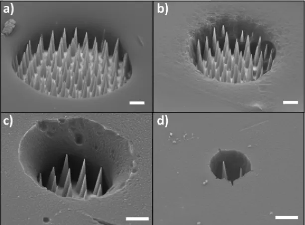
Fig. 2a shows the scanning electron micrographs of microelectrode surfaces. One can observe the ordered nanotips, which are surrounded by the insulating layer defining a disk area. By adapting the region of interest illuminated in the confocal mode, the final dimension of the microelectrode was tuned. Examples shown in Fig. 2 depict disk mi-croelectrodes which radius were estimated as: 3.5μm, 7μm, 12μm and 20μm, respectively (measurements on SEM images). The dimensions of the nanotips were constant but their number varied when we modified the radius of the microelectrode, i.e. the area of the exposed gold-coated surface. The 20-μm radius microelectrode (Fig. 2a) comprised ~105 nanotips whereas the smallest fabricated microelectrode of 3.5μm ra-dius consisted of only 4 exposed nanotips (Fig. 2d and corresponding top view in Fig. S1). Microelectrodes with larger dimensions can be eas-ily prepared as well by controlling the dimensions of the region of inter-est for the laser irradiation of the photoresist. Finally, it is noteworthy that a microelectrode array can also be obtained using such procedure. Indeed, we could illuminate sequentially several zones of the photore-sist on the bundle, allowing the removal of well-defined regions on the same sample, after the development step. For example, Fig. 3 displays the SEM image of two microelectrodes decorated with nanotips with a similar radius of 10±1μm. They were simply fabricated by illuminat-ing in confocal microscopy two distinct zones of the same etched optical fiber bundles initially covered by the insulating photoresist. However, both microelectrodes are electrically inter-connected in that case. They cannot be individually addressed by electrochemical means and their respective currents cannot be measured separately using the aforemen-tioned fabrication procedure.
UNCORRECTED
PROOF
4 T. Bombail et al. / Electrochimica Acta xxx (xxxx) 135105Fig. 2. SEM images of the fabricated nanotip microelectrodes with different radii: a) 20μm, b) 12μm, c) 7μm and d) 3.5μm. White scale bars: 5μm.
Fig. 3. SEM images of two nanotip microelectrodes fabricated by photolithography on the
same gold-modified etched substrate. White scale bar: 10μm.
3.2. Voltammetric characterization
The electrochemical responses of the nanotip microelectrodes were characterized by cyclic voltammetry. Ferrocenedimethanol was selected as a redox probe because of its well-established electrochemical prop-erties. Fig. 4 shows the voltammetric signals from the gold-coated nanotip microelectrodes shown in Fig. 2. All voltammetric responses are sigmoidal in shape indicating that nearly pure radial diffusion
Fig. 4. Cyclic voltammograms obtained with the gold nanotip microelectrodes of
differ-ent radii: a) 20μm, b) 12μm, c) 7μm and d) 3.5μm (SEM images in Fig. 2). The experi-ments were performed in an aqueous solution containing 1mM ferrocenedimethanol and 1M KNO3. Scan rate: 2mVs−1. (For interpretation of the references to color in this figure legend, the reader is referred to the Web version of this article.)
conditions were established, even with the nanotips decorating the sur-face of the microelectrode.
The electrochemical behavior of the nanotip microelectrodes was further investigated to understand the effects of the recessed
UNCORRECTED
PROOF
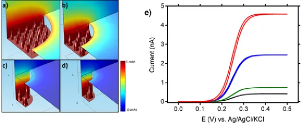
geometry and of the presence of the nanotips. The radius a of eachmi-croelectrode was determined from the SEM images. However, it was more difficult to measure on these the exact depth of the recess h, which is related to the thickness of the insulating photoresist layer. By exploit-ing the simulations, h value was estimated (Fig. S3). We compared the simulated voltammograms with the experimental data (Fig. 4) by ad-justing the value of h. The concentration profiles of the electrogener-ated oxidized species at E = +0.5 V vs. Ag/AgCl are also represented on Fig. 5a–d for the four different nanotip microelectrodes, respectively. The radius of the microelectrode, the recessed depth and the number of nanotips were chosen to correspond to the fabricated nanotip microelec-trodes (Fig. 2 and Fig. S1). The concentration profiles were simulated in the 3D geometry with a microelectrode surface decorated by the nan-otips. A gradient of concentrations, from 1mM to 0mM (coded as red and blue colors, respectively), is observed when moving away from the electrode surface. The shallow depth of the cavity allows the electrodes to maintain a radial diffusion layer that can clearly be observed in Fig. 5a and b. In Fig. 5c and d, the radial shape is retained even if it is less pronounced due to the higher depth of the cavity. Furthemore, the stationary state observed during cyclic voltammetry confirms the pres-ence of a radial diffusion layer. A linear diffusion would give a voltam-mogram with a peak shape, resulting from the increase of the diffusion layer thickness over time. Due to the difference of recessed depth for the different microelectrodes, differences of calculated concentrations observed at the exit of the cavity are higher for Fig. 5a and b (concen-tration~0.7mM, orange color coded) while they are lower for Fig. 5c and d conditions (concentration~0.2mM, blue color coded). The mass transport appears linear within the cavity, but, when taking into account the depth and the low scan rate used herein, the mass transport is domi-nated by the radial component outside the recess. As expected, the con-finement of the diffusion layer is more important when the depth of the recess microelectrode increases. This affects the value of the steady state current itip. The simulated voltammogram for each disk microelectrode
are represented in Fig. 5e.
The difference between the classical disk flat microelectrode and the recessed microelectrode has been studied numerous times in the litera-ture [65–67]. The deviation between the steady state currents of these two types of electrodes can be significant depending on the value of
h. For a microdisk with a radius of 7μm and a depth of 10μm, the
steady state current is almost three times lower than the one obtained for a classical microelectrode with the same radius (Fig. S3). When the surface of the recessed microelectrode is additionally structured
with nanotips, the steady state current increases. Indeed, the developed electroactive surface area is larger when the nanotips are present at the surface of the microelectrode. One can also observe on Fig. S3, that when the recess h is 4μm, for a equal to 20 and 12μm, the steady state current simulated for the configuration with the nanotips is very close to the one without the recess. It shows clearly that the effect of the recessed geometry affects much more the voltammetric responses than the pres-ence of the nanotips. This result is in agreement with previous works on lithography and shear-force positioning with such nanostructured elec-trodes [12,13].
3.3. Investigation of the SECM behavior
The electrochemical microscopy experiments were performed in feedback mode. In this mode the diffusion layer at the microelectrode can interact at short distances with the surface of the substrate. A suf-ficient anodic potential was imposed at the nanotip microelectrode to maintain a steady-state current itipusing ferrocenedimethanol as a
re-versible redox mediator. The microelectrode was moved toward the sub-strates at the rate of 1μms−1. The resulting approach curves correspond to the variations of the normalized microelectrode current, I=itip/itip,inf
(where itip,infis the current when the tip is positioned far away from the
substrate), with the normalized distance L=d/a (d is the distance be-tween the substrates and the microelectrode).
The experimental approach curves recorded with a nanotip micro-electrode have been compared (Fig. 6) to the theoretical approach curves simulated either for an insulating surface or for a conductive sub-strate. A glass slide was used as the insulating surface and a glassy car-bon electrode as the conductive surface. On the glass slide, the current measured at the tip decreases by reducing the distance between the mi-croelectrode and the insulator (Fig. 6). This current decreased is called a negative feedback mode. Indeed, the surface hinders the diffusion of the electroactive species that should react at the microelectrode surface. In contrast, on the glassy carbon electrode, when a potential of 0V is applied to consume the species generated at the microelectrode, the cur-rent increases when the distance L decreases because of the additional flux of the initial species provided by the glassy carbon surface that reach the nanotip microelectrode.
Both approach curves were realized with a nanotip microelectrode of 20μm radius, but the total diameter of the microelectrode was around 480μm. Our SECM microscope is equipped with an adjustable stage for the tilt correction that allows us to achieve such
Fig. 5. Schematic illustration of the simulated concentration profiles for microelectrodes decorated with recessed nanotips with different radii: a) 20μm, b) 12μm, c) 7μm and d) 3.5μm.
The shape and the size of the nanotips are constant but the number of electroactive nanotips varies. The geometric characteristics were extracted from the SEM pictures depicted on Fig. 2. Simulated diffusion layers of the oxidized species were calculated at E=0.5V. e) Corresponding simulated voltammograms for microelectrodes decorated with recessed nanotips with different radii: 20μm (red curve), 12μm (blue curve), 7μm (green curve) and 3.5μm (black curve). (For interpretation of the references to color in this figure legend, the reader is referred to the Web version of this article.)
UNCORRECTED
PROOF
6 T. Bombail et al. / Electrochimica Acta xxx (xxxx) 135105Fig. 6. SECM approach curves on (□) a glassy carbon electrode or (○) a glass slide using
a nanotip microelectrode of 20-μm radius at a scan rate of 1μms−1. The tip potential was set at 0.5V vs. Ag/AgCl/KCl 3M. The corresponding simulated approach curves on an in-sulating surface (blue curve) and on a conductive surface (red curve) are superimposed. (For interpretation of the references to color in this figure legend, the reader is referred to the Web version of this article.)
approach curves. These experiments prove that these new microelec-trodes are suitable for SECM experiments. Unlike to the classic disk mi-croelectrode probe, the approach curves for both negative and positive feedback modes are not only dependent on two dimensionless parame-ters, RG and L, RG being the diameter of the surrounding insulator di-vided by the radius a of the microelectrode. The value of rgis constant
(250μm) but, since we tuned the radius of the microelectrode in this work, the normalized parameter RG varies. In our simulations, we had to take into account the depth of the recessed microelectrode and the shape of the nanotips. These two geometrical features made more com-plex the modeling of currents but do not prevent from obtaining simu-lated approach curves. These experiments prove that these new micro-electrodes are suitable for SECM experiments. Furthermore the experi-mental curves are in good agreement with the simulated curves (Fig. 6). This study demonstrates that these new nanotips-decorated micro-electrodes can be used in an SECM configuration with the support of the simulations to analyze the experimental data.
Even if we successfully perform such SECM experiments, considering the large diameter of the probe, it can be difficult to approach it very close to a surface or to make in vivo studies using it. On the one hand, in previous reports, we used probes of similar sizes in SECM mode to pat-tern a surface or combined with shear-force positioning [12,13]. On the other hand, to make easier such in vivo experiments, it would be possible to decrease the global size of the bundle by heating-pulling techniques. As an example, a pulled and etched optical fiber bundle with a final ra-dius of 22μm is displayed in Fig. S4. It shows also that the aspect ratio of the nanotips is conserved.
3.4. SERS experiments
The capability to detect SERS signals with the developed nanotip microarrays was also investigated. Etched optical fiber bundles exhibit-ing a larger diameter (300μm) have already shown promisexhibit-ing capabil-ities as SERS-active substrates [47,48]. However, the presence of the surrounding photoresist film required to define a disk microelectrode could potentially affect the plasmonic behavior and lower the SERS efficiency. MBA was chosen as a model compound to record the Ra-man spectroscopic features because it is known to form stable monolay-ers on gold or silver metal surfaces [68,69]. Therefore, the thin gold
layer deposited on the microarray was modified with a MBA mono-layer by performing an overnight immersion and self-assembly with a 0.5mM MBA solution in ethanol. Fig. 7a shows a typical SERS
Fig. 7. a) Typical SERS spectra of MBA recorded on the gold-coated nanotip
microelec-trode (red line) and negative control on a non-structured zone (blue line). b) Confocal Ra-man mapping of the microelectrode functionalized with a MBA monolayer. The images are color-coded according to the intensity of the Raman band of MBA adsorbed species centred at 1591cm−1. c) Confocal Raman image (1.4μm×1.2μm) of an individual gold-coated nanotip modified with a MBA self-assembled monolayer. (For interpretation of the refer-ences to color in this figure legend, the reader is referred to the Web version of this arti-cle.)
UNCORRECTED
PROOF
spectrum recorded on a functionalized-nanotip microelectrode (647nm,0.09mW, 100×objective, N.A. 0.9). These data match perfectly with MBA characteristic spectrum, which displays two main features appear-ing as intense bands at 1078 and 1591cm−1and being assigned to ν8a and ν12 aromatic ring vibrations, respectively [68,69]. For compari-son, a Raman spectrum was also recorded from a MBA solution in pure ethanol (647nm, 10mW, 20×objective, N.A. 0.35, data not shown) and this spectrum was consistent with literature [68] showing the same two bands centred at 1099cm−1and 1600cm−1. It is noteworthy that the relative intensities of the vibration modes of the MBA molecules ad-sorbed on the nanostructured gold surface are indeed slightly different from that of the reference spectrum. The Raman enhancement factor, which directly originates from electromagnetic enhancement processes at the tip apex was calculated according to a previously reported method [48], and a typical value of 7±1×10⁴was found (see SI for details). The standard deviation originates from the tip-to-tip sharpness differ-ence based on a series of spectra recorded independently on 4 nanotips, thus modulating the intrinsic SERS efficiency. One can also observe that the background of the spectrum is significant though not limiting an-alytically, depicting a typical large broad feature assigned to fluores-cence and superimposed to the sharp Raman peaks. This background was not only observed on the nanotips (at the center of the disk microar-ray) but also on its border where the photoresist layer was not removed (Fig. 7b). We did not investigate in detail the nature of such a fluores-cence background as Raman signal could clearly be discriminated but it could be possibly due to some residual constituents of the photoresist layer. This potential issue could be solved by using some other insulat-ing materials such as fluorocarbon polymer thin films as demonstrated for the controlled positioning of analytes and cells on a plasmonic plat-form [70].
In addition to the recording of Raman spectra, high-resolution spa-tial-imaging measurements were also performed in order to study the influence of the XYZ position on the SERS substrates. The mapping of a series of nanotips was performed by recording step spectra every 150nm with an integration time of 3s. Fig. 7c shows the Raman intensity dis-tribution obtained by selecting the MBA typical band at 1591cm−1. This is indeed a representative image of a single tip optimized by varying the axial position (Z) and recorded on a 1.4μm×1.2μm 2D zone (XY). This data confirms that the Raman enhancement can be finely tuned along-side the tip with the maximum intensity perfectly matching the summit of each tip structure.
Moreover, in the optical configurations reported so far where SECM and Raman (or SERS) spectroscopy have been combined, the electro-chemical probes have to be manipulated and positioned under a Raman microscope [20,29,71]. It represents an experimental challenge to asso-ciate both microscopies in a single setup. With the dual probes proposed herein, the optical configuration for the SECM/SERS experiments may be different. Indeed, the developed probes are based on optical fiber bundles that guide light. In a previous report [47], we demonstrated the remote SERS sensing through such nanostructured bundles. The ex-citation laser was injected in the polished proximal face of the optical bundle. It was guided by total internal reflection in the individual fiber cores in order to be confined to the apex of the tips and induce a SERS effect. A fraction of the backscattered Raman signal at the tips is then collected by the same bundle, transmitted and detected back at the prox-imal face of the bundle. This optical configuration associated with the reported dual probes allows both Raman and SECM setups to be sepa-rated. Indeed, the Raman setup can operate at the proximal extremity of the bundle whereas SECM setup is located at the distal extremity.
Besides, the recessed geometry of the reported dual probes does not allow a priori to position them in the near-field of a given sub-strate or surface. It means that TERS or SERS imaging experiments of
immobilized molecules of interests at a living cell surface, for example, are not possible in this configuration. Indeed, the tips would be located too far from the surface to benefit from the plasmonic near field effects. However, this probe can detect freely-diffusing molecules by SERS. Mol-ecules that are released by cells [72,73] or (eletro)generated by a sur-face [74,75] diffuse and reach the nanotips where they are detected by SERS and/or by electrochemistry. In addition, it renders possible the study of the molecular functionalization and substitution dynamics of surfaces as well as the characterization of cellular release of biomole-cules [36,76]. In these cases, SECM mode can be used to position the probe or to examine surface reactivity while SERS sensing is devoted to the highly specific detection of free molecules in the surrounding liquid medium.
4. Conclusion
We prepared a new type of dual SECM/SERS platforms by combining the fabrication processes of scanning near-field optical probes with pho-tolithography. The resulting gold-coated microelectrodes decorated with optical nanotips were fabricated with tunable size. The sigmoidal shape of the steady-state voltammograms indicates that these opto-electro-chemical probes behave as microelectrodes with radial diffusion regime. Numerical simulations show that the recessed geometry governs mainly the voltammetric behavior whereas the presence of the nanotips influ-ences slightly the diffusional regime and the electrochemical responses. Such nanostructured microelectrodes are then used as SECM micro-probes in negative and positive feedback modes on insulating and con-ducting substrates, respectively. Finally, a SERS effect induced by the gold-coated nanotips was demonstrated by imaging a monolayer of a chemical probe adsorbed on the microelectrode surface by confocal Ra-man microscopy. Such dual platforms show distinct and complementary features for investigating complex microenvironments or in situ SERS studies of electrochemically induced processes. They could find a wide range of applications in photonic devices or electro-optical probes for biosensing, among which the detection of neurosecretory processes at single cells. Indeed, as shown recently [73], SERS performed at a nan-otip allows one to detect dynamically the cell release of certain neuro-transmitters which are not electroactive (glutamate, ATP), others being electroactive (dopamine) could be detectable by the electrode surface simultaneously. The combination of both methodologies on the same probe, of less than 100μm diameter, would provide unprecedented fea-tures for sensing, for instance, in the brain tissue different types of neu-ronal activities with high spatial accuracy.
Acknowledgements
We thank the Agence Nationale de la Recherche (Moly project, ANR-15-CE19-0005-02), University of Bordeaux, Bordeaux INP and CNRS for their financial supports.
Appendix A. Supplementary data
Supplementary data to this article can be found online athttps://doi. org/10.1016/j.electacta.2019.135105.
References
[1] A.J. Bard, M.V. Mirkin, Scanning Electrochemical Microscopy, second ed., CRC Press, 2012.
[2] M.V. Mirkin, F.-R.F. Fan, A.J. Bard, Scanning electrochemical microscopy part 13. Evaluation of the tip shapes of nanometer size microelectrodes, J. Elec-troanal. Chem. 328 (1992) 47.
[3] Q. Fulian, A.C. Fisher, G. Denuault, Applications of the boundary element method in Electrochemistry: scanning electrochemical microscopy, J. Phys. Chem. B 103 (1999) 4387–4392.
[4] Q. Fulian, A.C. Fisher, G. Denuault, Applications of the boundary element method in Electrochemistry: scanning electrochemical microscopy, Part 2, J. Phys. Chem. B 103 (1999) 4393–4398.
UNCORRECTED
PROOF
8 T. Bombail et al. / Electrochimica Acta xxx (xxxx) 135105[5] Y. Selzer, D. Mandler, Scanning electrochemical microscopy. Theory of the feedback mode for hemispherical Ultramicroelectrodes: steady-state and tran-sient behavior, Anal. Chem. 72 (2000) 2383–2390.
[6] C. Amatore, B. Fosset, Equivalence between microelectrodes of different shapes: between myth and reality, Anal. Chem. 68 (1996) 4377–4388.
[7] H. Xiong, D.A. Gross, J. Guo, S. Amemiya, Local feedback mode of scanning electrochemical microscopy for electrochemical characterization of one-dimen-sional Nanostructure: theory and experiment with nanoband electrode as model substrate, Anal. Chem. 78 (2006) 1946–1957.
[8] Y. Lee, S. Amemiya, A.J. Bard, Scanning electrochemical microscopy. 41. The-ory and characterization of ring electrodes, Anal. Chem. 73 (2001) 2261–2267. [9] E.M. Hussien, W. Schuhmann, A. Schulte, Shearforce-based constant-distance
scanning electrochemical microscopy as fabrication tool for needle-type car-bon-fiber nanoelectrodes, Anal. Chem. 82 (2010) 5900–5905.
[10] P. Sun, M.V. Mirkin, Scanning electrochemical microscopy with slightly re-cessed nanotips, Anal. Chem. 79 (2007) 5809–5816.
[11] A. Schulte, M. Nebel, W. Schuhmann, Scanning electrochemical microscopy in neuroscience, Annu. Rev. Anal. Chem. 3 (2010) 299–318.
[12] C. Adam, F. Kanoufi, N. Sojic, M. Etienne, Shearforce positioning of nanoprobe electrode arrays for scanning electrochemical microscopy experiments, Elec-trochim. Acta 179 (2015) 45–56.
[13] F. Deiss, C. Combellas, C. Fretigny, N. Sojic, F. Kanoufi, Lithography by scan-ning electrochemical microscopy with a multiscaled electrode, Anal. Chem. 82 (2010) 5169.
[14] F. Cortés-Salazar, D. Momotenko, H.H. Girault, A. Lesch, G. Wittstock, Seeing big with scanning electrochemical microscopy, Anal. Chem. 83 (2011) 1493–1499.
[15] J. Wiedemair, B. Balu, J.-S. Moon, D.W. Hess, B. Mizaikoff, C. Kranz, Plasma-deposited fluorocarbon films: insulation material for microelectrodes and combined atomic force Microscopy−Scanning electrochemical microscopy probes, Anal. Chem. 80 (2008) 5260–5265.
[16] P. Knittel, B. Mizaikoff, C. Kranz, Simultaneous nanomechanical and electro-chemical mapping: combining peak force tapping atomic force microscopy with scanning electrochemical microscopy, Anal. Chem. 88 (2016) 6174–6178. [17] A. Lesch, B. Vaske, F. Meiners, D. Momotenko, F. Cortés-Salazar, H.H. Girault,
G. Wittstock, Parallel imaging and template-free patterning of self-assembled monolayers with soft linear microelectrode arrays, Angew. Chem. Int. Ed. 51 (2012) 10413–10416.
[18] Y. Lee, A.J. Bard, Fabrication and characterization of probes for combined scan-ning electrochemical/optical microscopy experiments, Anal. Chem. 74 (2002) 3626–3633.
[19] R. Lei, L. Stratmann, D. Schäfer, T. Erichsen, S. Neugebauer, N. Li, W. Schuh-mann, Imaging biocatalytic activity of enzyme-polymer spots by means of com-bined scanning electrochemical microscopy/electrogenerated chemilumines-cence, Anal. Chem. 81 (2009) 5070.
[20] M. Etienne, M. Dossot, J. Grausem, G. Herzog, Combined Raman microspec-trometer and shearforce regulated SECM for corrosion and self-healing analysis, Anal. Chem. 86 (2014) 11203–11210.
[21] L. Wang, J. Kowalik, B. Mizaikoff, C. Kranz, Combining scanning electrochemi-cal microscopy with infrared attenuated total reflection spectroscopy for in situ studies of electrochemically induced processes, Anal. Chem. 82 (2010) 3139–3145.
[22] L. Wang, C. Kranz, B. Mizaikoff, Monitoring scanning electrochemical mi-croscopy approach curves with mid-infrared spectroscopy: toward a novel cur-rent-independent positioning mode, Anal. Chem. 82 (2010) 3132–3138. [23] K. Maruyama, H. Ohkawa, S. Ogawa, A. Ueda, O. Niwa, K. Suzuki, Fabrication
and characterization of a nanometer-sized optical fiber electrode based on se-lective chemical etching for scanning electrochemical/optical microscopy, Anal. Chem. 78 (2006) 1904–1912.
[24] F.-M. Boldt, J. Heinze, M. Diez, J. Petersen, M. Börsch, Real-time pH mi-croscopy down to the molecular level by combined scanning electrochemical microscopy/single-molecule fluorescence spectroscopy, Anal. Chem. 76 (2004) 3473–3481.
[25] S. Szunerits, N. Knorr, R. Calemczuk, T. Livache, New approach to writing and simultaneous reading of Micropatterns: combining surface plasmon resonance imaging with scanning electrochemical microscopy (SECM), Langmuir 20 (2004) 9236–9241.
[26] G. Premaratne, J. Niroula, M.K. Patel, W. Zhong, S.L. Suib, A.K. Kalkan, S. Kr-ishnan, Electrochemical and surface-plasmon correlation of a serum-autoanti-body immunoassay with binding insights: graphenyl surface versus mer-capto-monolayer surface, Anal. Chem. 90 (2018) 12456–12463.
[27] H. He, Z. Ding, D.W. Shoesmith, The determination of electrochemical reactiv-ity and sustainabilreactiv-ity on individual hyper-stoichiometric UO2+x grains by Ra-man microspectroscopy and scanning electrochemical microscopy, Electrochem. Commun. 11 (2009) 1724–1727.
[28] L. Guadagnini, C. Chiavari, C. Martini, E. Bernardi, L. Morselli, D. Tonelli, The use of scanning electrochemical microscopy for the characterisation of patinas on copper alloys, Electrochim. Acta 56 (2011) 6598–6606.
[29] J. Clausmeyer, M. Nebel, S. Grützke, Y.U. Kayran, W. Schuhmann, Local surface modifications investigated by combining scanning electrochemical microscopy and surface-enhanced Raman scattering, ChemPlusChem 83 (2018) 414–417. [30] M.E. Stewart, C.R. Anderton, L.B. Thompson, J. Maria, S.K. Gray, J.A. Rogers,
R.G. Nuzzo, Nanostructured plasmonic sensors, Chem. Rev. 108 (2008) 494–521.
[31] S. Cintra, M.E. Abdelsalam, P.N. Bartlett, J.J. Baumberg, T.A. Kelf, Y. Sugawara, A.E. Russell, Sculpted substrates for SERS, Faraday Discuss 132 (2006) 191. [32] M.E. Abdelsalam, S. Mahajan, P.N. Bartlett, J.J. Baumberg, A.E. Russell, SERS
at structured palladium and platinum surfaces, J. Am. Chem. Soc. 129 (2007) 7399–7406.
[33] J.N. Anker, W.P. Hall, O. Lyandres, N.C. Shah, J. Zhao, R.P. Van Duyne, Biosensing with plasmonic nanosensors, Nat. Mater. 7 (2008) 442–453. [34] K.A. Willets, R.P. Van Duyne, Localized surface plasmon resonance
spec-troscopy and sensing, Annu. Rev. Phys. Chem. 58 (2006) 267–297. [35] D. Kurouski, M. Mattei, R.P. Van Duyne, Probing redox reactions at the
nanoscale with electrochemical tip-enhanced Raman spectroscopy, Nano Lett. 15 (2015) 7956–7962.
[36] S. Zaleski, A.J. Wilson, M. Mattei, X. Chen, G. Goubert, M.F. Cardinal, K.A. Wil-lets, R.P. Van Duyne, Investigating nanoscale electrochemistry with surface-and tip-enhanced Raman spectroscopy, Acc. Chem. Res. 49 (2016) 2023–2030. [37] M. Fan, G.F.S. Andrade, A.G. Brolo, A review on the fabrication of substrates for
surface enhanced Raman spectroscopy and their applications in analytical chemistry, Anal. Chim. Acta 693 (2011) 7–25.
[38] R.J.C. Brown, M.J.T. Milton, Nanostructures and nanostructured substrates for surface - enhanced Raman scattering (SERS), J. Raman Spectrosc. 39 (2008) 1313–1326.
[39] L. Zhao, J. Blackburn, C.L. Brosseau, Quantitative detection of uric acid by elec-trochemical-surface enhanced Raman spectroscopy using a multilayered Au/Ag substrate, Anal. Chem. 87 (2015) 441–447.
[40] M. Atighilorestani, J.W. Menezes, A.G. Brolo, Large area plasmonic gold nanopillar 3-D electrodes, Electrochim. Acta 188 (2016) 91–97.
[41] F. Deiss, N. Sojic, D. White, P. Stoddart, Nanostructured optical fibre arrays for high-density biochemical sensing and remote imaging, Anal. Bioanal. Chem. 396 (2010) 53.
[42] G. Kostovski, D.J. White, A. Mitchell, M.W. Austin, P.R. Stoddart, Nanoim-printed optical fibres: biotemplated nanostructures for SERS sensing, Biosens. Bioelectron. 24 (2009) 1531.
[43] D.J. White, A.P. Mazzolini, P.R. Stoddart, Fabrication of a range of SERS sub-strates on nanostructured multicore optical fibres, J. Raman Spectrosc. 38 (2007) 377–382.
[44] D.J. White, P.R. Stoddart, Nanostructured optical fiber with surface-enhanced Raman scattering functionality, Opt. Lett. 30 (2005) 598–600.
[45] M. Fan, P. Wang, C. Escobedo, D. Sinton, A.G. Brolo, Surface-enhanced Raman scattering (SERS) optrodes for multiplexed on-chip sensing of nile blue A and oxazine 720, Lab Chip 12 (2012) 1554–1560.
[46] G.F.S. Andrade, M. Fan, A.G. Brolo, Multilayer silver nanoparticles-modified op-tical fiber tip for high performance SERS remote sensing, Biosens. Bioelectron. 25 (2010) 2270.
[47] V. Guieu, P. Garrigue, F. Lagugné-Labarthet, L. Servant, N. Sojic, D. Talaga, Re-mote surface enhanced Raman spectroscopy imaging via a nanostructured opti-cal fiber bundle, Opt. Express 17 (2009) 24030.
[48] V. Guieu, D. Talaga, L. Servant, N. Sojic, F. Lagugne-Labarthet, Multitip-local-ized enhanced Raman scattering from a nanostructured optical fiber array, J. Phys. Chem. C 113 (2009) 874–881.
UNCORRECTED
PROOF
[49] V. Guieu, F. Lagugné-Labarthet, L. Servant, D. Talaga, N. Sojic, Ultrasharpopti-cal-fiber nanoprobe array for Raman local-enhancement imaging, Small 4 (2008) 96–99.
[50] P. Pantano, D.R. Walt, Ordered nanowell Arrays, Chem. Mater. 8 (1996) 2832–2835.
[51] P. Pantano, D.R. Walt, Toward a near-field optical array, Rev. Sci. Instrum. 68 (1997) 1357–1359.
[52] P. Pantano, D.R. Walt, Analytical applications of optical imaging fibers, Anal. Chem. 67 (1995) 481A–487A.
[53] M. Zamuner, D. Talaga, V. Guieu, F. Deiss, A. Kuhn, P. Ugo, N. Sojic, Multi-scaled nanostructured array fabricated on an etched imaging bundle for sur-face-enhanced Raman scattering, Adv. Funct. Mater. 19 (2009) 3129–3135. [54] H. Aouani, F. Deiss, J. Wenger, P. Ferrand, N. Sojic, H. Rigneault,
Opti-cal-fiber-microsphere for remote fluorescence correlation spectroscopy, Opt. Ex-press 17 (2009) 19085.
[55] S. Szunerits, J.M. Tam, L. Thouin, C. Amatore, D.R. Walt, Spatially resolved electrohemiluminescence on an array of electrode tips, Anal. Chem. 75 (2003) 4382–4388.
[56] A. Chovin, P. Garrigue, N. Sojic, Remote NADH imaging through an ordered ar-ray of electrochemiluminescent nanoapertures, Bioelectrochem. 69 (2006) 25–33.
[57] A. Chovin, P. Garrigue, P. Vinatier, N. Sojic, Development of an ordered array of optoelectrochemical individually readable sensors with submicrometer di-mensions: application to remote electrochemiluminescence imaging, Anal. Chem. 76 (2004) 357–364.
[58] A. Chovin, P. Garrigue, N. Sojic, Electrochemiluminescent detection of hydro-gen peroxide with an imaging sensor array, Electrochim. Acta 49 (2004) 3751–3757.
[59] A. Chovin, P. Garrigue, I. Manek-Hönninger, N. Sojic, Fabrication, characteriza-tion and far-field optical properties of an ordered array of nanoapertures, Nano Lett. 4 (2004) 1965–1968.
[60] N. Godino, X. Borrisé, F.X. Muñoz, F.J. del Campo, R.G. Compton, Mass trans-port to nanoelectrode arrays and limitations of the diffusion domain approach: theory and experiment, J. Phys. Chem. C 113 (2009) 11119–11125. [61] M. Ohtsu, Progress of high-resolution photon scanning tunneling microscopy
due to a nanometric fiber probe, J. Light. Technol. 13 (1995) 1200–1221. [62] G. Krausch, S. Wegscheider, A. Kirsch, H. Bielefeldt, J.C. Meiners, J. Mlynek,
Near field microscopy and lithography with uncoated fiber tips: a comparison, Opt. Commun. 119 (1995) 283–288.
[63] M. De Serio, R. Zenobi, V. Deckert, Looking at the nanoscale: scanning near-field optical microscopy, Trends Anal. Chem. 22 (2003).
[64] R. Micheletto, N. Yoshimatsu, S. Okazaki, A simple method for the fabrication of low cost scanning near field optical microscope probes with acrylic paint as coating element, Opt. Commun. 188 (2001) 11–15.
[65] P.N. Bartlett, S.L. Taylor, An accurate microdisc simulation model for recessed microdisc electrodes, J. Electroanal. Chem. 453 (1998) 49–60.
[66] R. Ferrigno, P.F. Brevet, H.H. Girault, Finite element simulation of the chronoamperometric response of recessed and protruding microdisc electrodes, Electrochim. Acta 42 (1997) 1895–1903.
[67] A.M. Bond, D. Luscombe, K.B. Oldham, C.G. Zoski, A comparison of the chronoamperometric response at inlaid and recessed disc microelectrodes, J. Electroanal. Chem. 249 (1988) 1–14.
[68] A. Michota, J. Bukowska, Surface-enhanced Raman scattering (SERS) of 4-mer-captobenzoic acid on silver and gold substrates, J. Raman Spectrosc. 34 (2003) 21–25.
[69] H. Park, S.B. Lee, K. Kim, M.S. Kim, Surface-enhanced Raman scattering of p-aminobenzoic acid at silver electrode, J. Phys. Chem. 94 (1990) 7576–7580. [70] M. Tabatabaei, G.Q. Wallace, F.A. Caetano, E.R. Gillies, S.S.G. Ferguson, F.
Lagugne-Labarthet, Controlled positioning of analytes and cells on a plasmonic platform for glycan sensing using surface enhanced Raman spectroscopy, Chem. Sci. 7 (2016) 575–582.
[71] M. Steimecke, G. Seiffarth, M. Bron, In situ characterization of Ni and Ni/Fe thin film electrodes for oxygen evolution in alkaline media by a Raman-coupled scanning electrochemical microscope setup, Anal. Chem. 89 (2017)
10679–10686.
[72] R.J. Dijkstra, W.J.J.M. Scheenen, N. Dam, E.W. Roubos, J.J. ter Meulen, Moni-toring neurotransmitter release using surface-enhanced Raman spectroscopy, J. Neurosci. Methods 159 (2007) 43–50.
[73] F. Lussier, T. Brulé, M.-J. Bourque, C. Ducrot, L.-É. Trudeau, J.-F. Masson, Dy-namic SERS nanosensor for neurotransmitter sensing near neurons, Faraday Discuss 205 (2017) 387–407.
[74] C. Amatore, F. Bonhomme, J.-L. Bruneel, L. Servant, L. Thouin, Mapping con-centration profiles within the diffusion layer of an electrode Part I. Confocal resonance Raman microscopy, Electrochem. Commun. 2 (2000) 235–239. [75] C. Amatore, F. Bonhomme, J.-L. Bruneel, L. Servant, L. Thouin, Mapping
dy-namic concentration profiles with micrometric resolution near an active micro-scopic surface by confocal resonance Raman microscopy. Application to diffu-sion near ultramicroelectrodes: first direct evidence for a conproportionation re-action, J. Electroanal. Chem. 484 (2000) 1–17.
[76] M. Plissonneau, A. Madeira, D. Talaga, S. Bonhommeau, L. Servant, R.A.L. Val-lée, C. Labrugère, I.A. Goldthorpe, L. Pautrot-D’Alencon, T. Le Mercier, M. Treguer-Delapierre, Efficient passivation of Ag nanowires with 11-mercap-toundecanoic acid probed using in situ total-internal-reflection surface-en-hanced Raman scattering spectroscopy, ChemNanoMat 5 (2019) 1044–1049.