HAL Id: hal-02304951
https://hal.archives-ouvertes.fr/hal-02304951
Submitted on 25 Nov 2020HAL is a multi-disciplinary open access archive for the deposit and dissemination of sci-entific research documents, whether they are pub-lished or not. The documents may come from teaching and research institutions in France or abroad, or from public or private research centers.
L’archive ouverte pluridisciplinaire HAL, est destinée au dépôt et à la diffusion de documents scientifiques de niveau recherche, publiés ou non, émanant des établissements d’enseignement et de recherche français ou étrangers, des laboratoires publics ou privés.
Pendeo-epitaxy of GaN on SOI nano-pillars:
Freestanding and relaxed GaN platelets on silicon with a
reduced dislocation density
Roy Dagher, Philippe de Mierry, Blandine Alloing, Virginie Brandli, Marc
Portail, Benjamin Damilano, Nicolas Mante, Nicolas Bernier, Patrice
Gergaud, Maximilien Cottat, et al.
To cite this version:
Roy Dagher, Philippe de Mierry, Blandine Alloing, Virginie Brandli, Marc Portail, et al.. Pendeo-epitaxy of GaN on SOI nano-pillars: Freestanding and relaxed GaN platelets on silicon with a reduced dislocation density. Journal of Crystal Growth, Elsevier, 2019, 526, pp.125235. �10.1016/j.jcrysgro.2019.125235�. �hal-02304951�
Pendeo-epitaxy of GaN on SOI nano-pillars: freestanding and relaxed GaN platelets
on silicon with a reduced dislocation density
Roy Dagher1*, Philippe de Mierry2, Blandine Alloing2, Virginie Brändli2, Marc Portail2, Benjamin Damilano2,
Nicolas Mante1, Nicolas Bernier1, Patrice Gergaud1, Maximilien Cottat3, Cécile Gourgon3, Jesus Zuniga Perez2
and Guy Feuillet1
1
Université Grenoble Alpes, CEA-LETI, 17 Rue Des Martyrs, 38054 Grenoble, France 2Université Côte d’Azur, CRHEA-CNRS, Rue Bernard Gregory, 06560 Valbonne, France 3
Université Grenoble Alpes, CNRS LTM, 17 Rue Des Martyrs, 38054 Grenoble, France *E-mail: roy.dagher2@cea.fr
Nanopendeo-epitaxy of gallium nitride (GaN) is considered in this study as a way of producing freestanding GaN with reduced strain and threading dislocation density (TDD) for optoelectronic applications. The novelty of this work lies in the use of silicon on insulator (SOI) substrates patterned into nano-pillars down to the buried oxide (BOX). We actually want to benefit from the creeping properties of SiO2 at the growth temperature of GaN
for strain relaxation and grain-boundary dislocations reduction. In this paper, we report on the fabrication of 40×40 µm2 and 300×300 µm2 freestanding GaN platelets, up to 10 µm-thick, spontaneously separated from the
initial pillars. Structural and optical characterizations show that the platelets are crack-free and almost fully relaxed, with a TDD of ∼ 4×10⁸/cm2. We underline the different benefits of this approach, but most importantly,
we believe that it will be the founding-brick for transferable GaN-based devices.
Keywords: A1. Defects, A1. Nanostructures, A3. Metalorganic vapor phase epitaxy, A3. Pendeo-Epitaxy, B1. Gallium nitride, B1. Silicon on insulator.
I. Introduction
The efficiency of gallium nitride based light emitting diodes (LEDs) and laser diodes, as well as their lifetime, depends strongly on the dislocation density of the grown material [1,2], especially since threading dislocations (TD) can act as non-radiative centers. Unfortunately, bulk GaN is still of low dimension, expensive and far from being perfect. At the same time, GaN heteroepitaxy on sapphire, silicon or silicon carbide still suffers of a number of issues such as the high threading dislocation density due to
the large lattice mismatch, and the appearance of cracks due to the thermal expansion coefficients (TEC) mismatch between the GaN epilayer and the foreign substrate (in the case of silicon). The standard approach to deal with this latter issue, in the case of silicon substrates, consists in stacking a series of AlGaN-based interlayers leading to complex heterostructures before the device active region is grown.
© 2019. This manuscript version is made available under the Elsevier user license https://www.elsevier.com/open-access/userlicense/1.0/
Version of Record: https://www.sciencedirect.com/science/article/pii/S0022024819304506 Manuscript_5fb3217833f319814c12cc102dc0465c
2 One way to get around these problems is to reduce the footprint of the epilayer on the substrate, i.e. by minimizing the nucleation areas as much as possible, ergo reducing the number of dislocations originating from the substrate/nuclei interface. To reach such objective one can rely on methods such as nano-wires growth (NW) [3,4] or selective area growth (SAG) on patterned substrates with dielectric masks [5,6]. Alternative strategies rely on the anisotropic growth of the GaN planes to achieve lateral growth through a dielectric mask, including epitaxial lateral overgrowth (ELO) [7,8], or without a mask, such as pendeo-epitaxy (PE) [9,10].
These growth approaches are in principle advantageous but bring other issues to deal with such as an inhomogeneous TD distribution, concentrated in the window region (e.g. in the case of ELO) [8] and/or at the coalescence boundaries between crystallites coming from different nucleation sites (e.g. for PE) [11]. Even if this latter source of TD is rarely mentioned, it is an important and inevitable contribution to the TDD. In fact, neighboring crystallites approaching each other from independent nucleation sites inherit necessarily the crystallographic misalignment associated to the heteroepitaxial growth. This was demonstrated by N. Mante et al. [12] for aluminum nitride (AlN) grown on silicon, where AlN grains were found to be twisted with respect to each other with an in-plane misorientation of up to ± 3°; this misalignment results in the generation of coalescence boundary dislocations required to accommodate the misorientation. The dislocations will thread within the epilayer up to the active region, leading to an inhomogeneous spatial distribution of
stress and dislocation density dictated by the geometry of the initial pattern, as has been demonstrated in few studies [10,13].
To overcome the misalignment problem we need to give crystallites the freedom to twist and tilt around their growth axis in order to align themselves, thereby preventing the formation of boundary dislocations. To do so, one can imagine placing the crystallites on top of deformable nano-pillars that will act as “rotating” nano-pedestals. In this paper, we report pendeo-epitaxy on nano-patterned SOI substrates that are aimed to act as such nano-pedestals: we will take advantage of the creeping properties of SiO2 at the
growth temperature of GaN (∼1000°C) to reach our goal. In other words, the SiO2 will act as a
visco-elastic material, which will be pliant enough at 1000°C to deform. Indeed, if the dimensions of the pedestals are small enough and the growth temperature high enough, it should be energetically favorable for them to rotate rather than to generate new dislocations at the coalescence boundaries.
In addition, the use of deformable SOI nano-pillars has other benefits, such as drastically reducing the strain in the GaN epilayer and achieving freestanding GaN films sitting on an array of broken nano-pillars, hence opening new opportunities for device transfer. Indeed, J. Cao et al. [14] have considered SOI for the growth of GaN applying what they refer to as the compliant substrate approach. The idea consists of growing a thick lattice-mismatched epilayer on a thin compliant layer rigidly bound to the substrate. In the case of SOI, the top Si represents the so-called compliant layer. J. Cao et al. argue that if the substrate
3 is much thinner than the epilayer, it will accommodate most of the total strain. However, we believe that this behavior is more effective when the compliant substrate is nano-patterned. Indeed, in the present work, we expect the compliant SOI nano-pillars to accommodate the strain and, thanks to the use of an adequate aspect ratio (height/width), to break and release the GaN film.
As detailed later on, our approach consists first on nano-patterning the SOI templates with nano-imprint lithography and then transferring the design with top-down etching methods to create nano-pillars. The nano-pillars are etched down into the BOX to benefit from its visco-elastic properties at the growth temperature of GaN (around 1100°C). We will show the patterning steps and the two-step pendeo-epitaxial growth of a fully coalesced two-dimensional GaN layer. The threading dislocation density is evaluated by atomic force microscopy (AFM), transmission electron microscopy (TEM) and cathodoluminescence (CL), whereas strain is assessed with room-temperature photoluminescence (PL) and micro X-ray diffraction (XRD).
II. Experimental details
For this study, 2’’ SOI substrates with a 50 nm-thick <111> oriented Si “device” layer were used. After a chemical surface preparation to remove any native oxide, a 100 nm-thick AlN layer was grown on the full wafer followed by the growth of a 200 nm-thick GaN layer by metal organic vapor phase epitaxy (MOVPE) in a (6 x 2 in.) close-coupled showerhead (CCS) Aixtron 6 reactor. The growth of AlN on the Si surface was essential to avoid melt-back etching due to
the direct contact between Ga and Si [15]. The 200 nm thick GaN layer is found to have a TDD of about 9×10⁹/cm2, as measured with AFM. A protective 35
nm-thick SiO2 layer was then deposited on the GaN by
physical vapor deposition. Nanoimprint lithography was then adapted to define a hard etch nickel mask, followed by dry etching with Cl/CH4/Ar plasma to
transfer the pattern into the GaN templates reaching the BOX. Hence, a GaN/AlN/SOI nano-pillars array with hexagonal symmetry was defined over areas of 300×300 and 40×40 µm2. The dimensions of the
nano-pillars are 200 nm in width, ~ 450 nm in depth (Aspect ratio 2:1) and a 1000 nm-pitch (center-center distance). Figure 1(a) presents a scanning electron microscopy (SEM) image of the nano-pillars array after removal of the nickel mask and of the protective SiO2 layer with H2SO4 and HF solutions respectively.
It is possible to distinguish the GaN layer (dark contrast) from the AlN layer (light contrast) and the SiO2 pedestal, which has been under-etched by the HF
solution. We also notice in Figure 1(a) that the pillars sidewalls are not straight. One possible explanation can be the fact that the etching rate of the different layers in the stack is not the same; though, this is not of big concern, as it does not seem to affect the growth in any way.
Subsequently, using a MOVPE (3 x 2 in.) CCS Thomas Swan reactor, GaN was selectively grown in a two step-process on top of the GaN/AlN/SOI pillars using trimethylgallium (TMGa) and ammonia (NH3) as precursors, and H2 as carrier gas. The temperature
was monitored with an in-situ thermocouple below the susceptor. The growth process was carried out in two steps: the nucleation step (step 1) and the coalescence
4 step (step 2). During step 1, GaN pyramids are selectively grown on top of the pillars at 1135°C, 100 Torr and a V/III ratio of 1850 (see SEM images in Figure 1(b, c)). Step 1 was continued until adjacent pyramids came into contact. This exact moment of contact was calibrated by doing different tests with step 1 conditions only. This step was then followed by step 2 (1180°C, 300 Torr and a V/III ratio of 2100), where lateral growth is favored in order to promote the coalescence of the GaN pyramids and form a two-dimensional GaN layer (see Figure 1(d, e)). Figure 1(e) shows a 300×300 µm2 fully coalesced
freestanding GaN platelet with growth times of 160 s (step 1) and 5400 s (step 2). Figure 1(g) shows a 40×40 µm2 platelet with a longer step 2. Figure 1(f)
presents nine 300×300 µm2 GaN platelets separated by
1 mm in both directions. We will discuss in more details these observations in the following section.
These platelets are then investigated with SEM (Zeiss supra), AFM in tapping mode (Veeco dimension III setup) for structural characterization, along with cathodoluminescence (CL - JEOL 7000F SEM equipped with a Gatan Mono CL4 module) to detect non-radiative centers. Room-temperature micro photoluminescence (µ-PL) was used to assess the strain state in the final GaN layer by measuring the free-exciton emission energy. The laser source for PL is a frequency-doubled Ar laser at 244 nm with an excitation power of 30 mW. The AFM data were processed using WSxM software [16], whereas panchromatic CL images were analyzed with ImageJ [17]. To complement PL results, X-ray diffraction measurements with a 100 µm lateral resolution (µ-XRD) were performed on the GaN (006)
reflection (2θ around 126°) on a Rigaku SmartLab® diffractometer. Since a Goebel mirror was used to condition the incident beam, both Kα1 and Kα2 wavelengths are observed. The Kα2 ray was not filtered out to get the maximum possible incident intensity and have a good counting statistics. Finally, to evaluate the defects distribution and the pillars state after the 2D-film growth, weak-beam TEM and high-angle annular dark-field (HAADF) scanning transmission electron microscopy (STEM) images were acquired in a TEM FEI Titan Themis operated at 200 kV, along with the associated energy-dispersive X-ray spectroscopy (EDX) mappings. In the following, all the characterizations presented are performed on the 300×300 µm2 platelets.
III. Results and discussion
A. Structural Characterization and TDD In Figure 1, we show a side view (Figure 1(b)) and a top view (Figure 1(c)) of GaN-grown pyramids using step 1 only. The pyramids are ~ 920 nm-high and ~ 930 nm-wide and present six facets (Figure 1(c)) due to the anisotropic growth rate of GaN in the <11-20> (fast) and <1-100> (slow) directions, which leads to the formation of facets in the slowest growing direction and hexagonal apexes in the <11-20> direction at the facets intercepts. It is interesting to note that in an early study reported by Huang et al [18] parasitic growth was detected between the pillars. This can produce stacking faults (SF) terminated by partial dislocations after coalescence; however, it does not seem to be the case in the present study. Fully coalesced GaN platelets are presented in Figure 1(d-g). Figure 1(d) shows clearly the GaN film in
cross-5 section sitting on an array of visible nano-pillars indicated with red arrows. It is also possible to see some marginal parasitic deposition on the SiO2 around
the GaN platelets in Figure 1(e) (white arrows). Fortunately, these depositions do not interfere with the platelet growth, which is surrounded by an almost growth-free zone within the diffusion length of Ga ad-atoms. For the same reason, the large GaN platelets are much thicker at the edges (~ 13 µm-thick) than at the center (~ 5µm-thick) (see Figure 1(e)). However, a homogeneous thickness extends around the center over an area of 200×200 µm2. In fact, the growth in the
center region of the platelet proceeds thanks to ad-atoms adsorbed directly on the GaN pillars and, at later stages, on the platelet itself. On the other hand, at the edges of the pillar arrays, an additional supply of Ga ad-atoms coming from the surrounding SiO2 can
also be participating to the growth (in the limit of their diffusion length), hence the thicker growth at the edges of the platelets. This has been clearly demonstrated and formalized in reference [19] in the case of GaN stripes. It was shown that Ga ad-atoms have diffusion lengths up to 20 µm in similar growth conditions to ours, under a H2 atmosphere. In good agreement with
this reasoning, the thickness uniformity for the smaller platelets (40×40 µm2) in Figure 1(g) is much better,
with no thicker edges.
It should be noted that in some platelets (Figure 1(e, g)) we detect large holes (5-10 µm-large), indicated by black arrows and smaller holes (1-2 µm), at the center, indicated by red arrows. These holes have the shape of V-pits; however, we distinguish between two types of holes: the ones at the center, which are incomplete coalescences that can be
eliminated by increasing the growth time, and the ones at the edge (the larger holes in Figure 1(e)). The fact that these latter are observed on the thicker regions of the larger platelets, i.e. the edges, suggest that they might be correlated to the presence of a frontier between regions of different growth rates mainly related to the diffusion length of Ga ad-atoms deposited on the surrounding SiO2. In all cases, the
inner homogenous zone is about 200×200 µm2 in
Figure 1(e), hence large enough to be exploited for characterizations. Interestingly, there are no signs of cracks, even when we continue the growth to reach 10 µm-thick platelets (Figure 1(g)).
A closer look on a single pillar with a GaN pyramid before coalescence is shown in Figure 2(a, b). We can clearly distinguish the different layers beneath the pyramid, i.e. from bottom to top, the silicon wafer, the SiO2 layer of the BOX, the SiO2 pillar (130
nm-high), the thin layer of silicon and the GaN pyramid. It is clear in these latter figures that the growth of GaN not only takes place on the top GaN layer but also on the side facets of the AlN layer. After coalescence, cross-sectional TEM was performed on a lamella cut with focused ion beam (FIB) from a GaN platelet. A STEM image of a single pillar after coalescence is presented in Figure 2(c) accompanied with its EDX analysis in Figure 2(d). GaN has grown laterally on AlN but also partially on the Si layer. From the STEM image centered on the pillar, one can distinguish dislocations propagating horizontally from the vertical GaN/AlN interface (indicated by blue arrows), as well as dislocations propagating vertically from the horizontal GaN/AlN interface (indicated by red arrows). Note also the small fracture line in the SiO2
6 portion of the pillar indicated by a white arrow in Figure 2(c).
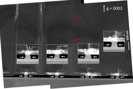
To better analyze the dislocations behavior, weak-beam TEM has been used, as presented in Figure 3, where a wider view of the coalesced layer is shown. The better contrast due to the weak-beam condition allows one to observe the high density of the laterally propagating dislocations originating from each pillar as well as the fracture line at the SiO2 level, indicated
with white arrows. Second, most of the dislocations propagating vertically from the GaN/AlN interface end up bending laterally into the c-plane. This is the well documented effect occurring during 3-dimensional growth of GaN [5]. The reader should keep in mind that the FIB lamella analyzed by TEM is about 200 nm-thick, meaning that additional dislocations might be located elsewhere within the depth associated to the 1000 nm-pitch.
We can now focus on the boundaries between crystallites nucleating on neighboring pillars. It is noteworthy that no emerging (threading) dislocations are visible between the three pillars on the right side of the image. Still, some defect-associated contrast is apparent for the other pillars on the left. Note as well that the white contrast indicated by red arrows could be a difference in contrast due to either strain variation or the presence of a dislocation nearby. We assume that the absence of, at least some, grain-boundary dislocations could be a first hint of pyramids coalescing together after a certain rotation odescf the pliable SiO2 pillars, accommodating thereby their
relative misorientation. We can indeed expect the pillars to twist and/or tilt in order to allow a perfect alignment of the crystallites rather than forming a
higher energy defective interface. This behavior is well known and documented for nanoparticles and crystal grains, which tend to rotate to achieve an energetically stable coalescence [20–22]. Nevertheless, one should keep in mind that other dislocations might be present in the depth of the FIB lamella and that this TEM image, even though interesting, is not enough to assess quantitatively a reduction in threading dislocations. Other techniques such as AFM and/or CL are required, as presented in the following paragraphs. It should be also underlined that since pillars (hence, pyramids) in the current pattern are equidistant, the described rotation mechanism can only operate to diminish dislocations between a certain fraction of crystallites. Actually, as soon as crystallites begin to coalesce, the total mass to be rotated becomes larger and larger; hence, rotation becomes unfavorable from an energetic point of view. In this last situation, a defective grain boundary will be favorable, generating threading dislocations.
Besides, fracture lines at the SiO2 level can be
clearly seen in Figure 3 (white arrows), and in the insets of Figure 3, where we did a zoom-in on the pillars and enhanced the contrast. We attribute this behavior to the compliant substrate principle described by J. Cao et al. in reference[14] , where the compliant SOI accommodates the built-up strain rising from the difference in TEC between the GaN film and the underlying Si substrate. As a result, and thanks to a sufficiently large 2:1 aspect ratio, the SOI pillars crack. This phenomenon releases the GaN platelet from its base and prevents the cracking of the platelet itself. For this reason, we expect an important reduction of strain in the GaN film, as the underlying
7 substrate is no longer attached to the platelets. Note that besides the force exerted on the pillars during the cooling-down due to the TEC difference, additional stresses can also develop on the pillars at the coalescence stage, which can further contribute to the pillars cracking.
AFM investigations of the GaN platelet reveal a smooth surface with a roughness of 0.6 nm in a 5×5 µm2 area (Figure 4(a)) and a threading dislocation
density of ∼ 4×10⁸/cm2. This is the average value
deduced from a number of 2×2 µm2 AFM images (e.g.
figure in inset displays a TDD of ∼3.5×10⁸/cm2). This
is confirmed with the panchromatic CL image in Figure 4(b) taken at 5 kV, which reveals dark spots associated with TDs acting as non-radiative centers. From this 28×28 µm2 CL image, and using the ImageJ
software, we are able to estimate a non-radiative TDD of ∼ 2.4×10⁸/cm2, which is roughly a factor 2 smaller
than the TDD measured by AFM and consistent with previous reports discussing TDD quantification [23].
These results are better than the standard case of GaN/silicon growth [24,25], i.e. in the absence of interlayers, which results in a TDD in the order of 109/cm2. Furthermore, the achieved TDD is similar to
studies in the literature using related defect-reducing approaches on sapphire substrates, such as PE [11] or ELO, [26] which report a TDD ∼ 4×10⁸/cm2.
However, as mentioned in these studies the TDD density can vary from one region to another, especially for the ELO technique, where dislocations are concentrated above the window (i.e. mask-opening) region. In contrast, the dislocation density observed in
Figures 4(a) and 4(b) is found to be uniformly distributed on the surface.
A second important observation concerns the strong TDD reduction after the first hundreds of nanometers. As revealed by the TEM image in Figure 3, most of the threading dislocations generated at the horizontal GaN/AlN interface bend after about 600 nm, which matches the size of the initial pyramids. Thus, the final TDD of about ∼ 4×10⁸/cm2
detected after several micrometers might be achievable for thicknesses below 1 micrometer, increasing further the technological prospects of the current approach.
B. Strain state evaluation
PL is a straightforward technique to evaluate the strain in GaN films by measuring the free-exciton emission energy. In fact, the emission energy of nitrides is very sensitive to the strain state: for (0001) GaN the deformation potential is ∼ -9 eV per % of biaxial in-plane strain [27,28]. To this end, room-temperature µ-PL measurements with an incident beam size ∼2 µm were carried out on a GaN platelet (300×300 µm2), as presented in Figure 5(a). The scan
was performed from the edge to the center of the platelet with a measurement step of 2 µm near the edge and 10 µm at the center, since we expected a stronger strain gradient near the edge. The figure in inset shows the free-exciton (FE) emission energy and its intensity at different positions. The FE peak position varies around 3.419 eV (linewidth: 52 meV), but tends towards 3.418 eV at the edge region. The intensity seems higher in this same area, which could be just due to a better photon extraction through the platelet free edges. In addition, another emission is
8 detected forming a shoulder at 3.352 eV, attributed to the first LO phonon replica, since its energy separation from the free-exciton emission is equal to ELO –
3/2(kT), ELO being the energy of the longitudinal
optical phonon in GaN [29]. It should be noted that 5kV CL measurements (not presented here) show similar emission spectra.
Assuming a purely biaxial deformation state, one can estimate the biaxial in-plane deformation value using the band-gap emission energy from PL data and the following relation [3,27]:
= + × (1)
where is the strain-free exciton energy and the GaN deformation potential (-9 per % ± 1 eV) [27,28]. The main issue for this estimation is the large discrepancy found in the literature concerning the strain-relaxed FE energy at 300 K (see Figure 6(a) and associated references). A similar situation is encountered when dealing with the strain-free lattice parameter of GaN, as resumed in Figure 6(b) (see associated references). For this reason, we present the different values extracted from the literature associated to strain-free GaN in Figure 6(a) and (b), compared to our data (red data). The meshed areas correspond to the strain-free area. In Figure 6(a), the tensile strain area (resp. compressive) extends between the meshed area and the silicon reference (resp. sapphire reference) at 3.387 eV (resp. 3.426 eV). We notice that our µ-PL data is in the compressive area. However, compressive strain is unexpected, since GaN films on silicon are usually under tensile strain. In all cases, our measured data suggest a more relaxed GaN film (at the
surface) compared to standard GaN on silicon or sapphire (see Figure 6(a)), or even with intermediate AlGaN and AlN buffer layers (at 3.39 eV).
Given the penetration depth of the excitation laser, limited to about 200 nm, the PL technique enables to evaluate only the strain state close to the surface. To probe the overall strain state of the platelet, i.e. to average over the whole platelet thickness, micro X-ray diffraction has been employed. The scan is carried out with a step size of 100 µm and a beam size of ∼ 500×150 µm2. It is possible to know that the beam is
on the platelet by scanning the sample along the platelets axis and monitoring the diffracted intensity of a certain reflection. The 2θ-ω scan of the most intense GaN (0006) reflection is shown in Figure 5(b). In this figure, we detect two reflection rays corresponding to Kα1 and Kα2. The most intense peak at the low-angle side is at 126.08° with a FWHM of 0.174°. Using the well-known relation between the c lattice constant and the peak position (126.08°), we can estimate a c lattice constant of 5.1853 Å [3,30]. We can now compare with the strain-free lattice parameter of GaN. However, as for the emission energy, there is a large discrepancy for the strain-free lattice parameters depending on the preparation method of GaN [31]. For this reason, in Figure 6 (b) we present a similar approach as before but now for the c-lattice parameter. Using our estimated c lattice parameter (5.1853 Å), we can deduce that we are in the meshed region considered as strain-free. This result is different compared to PL estimations, which can be attributed to the difference in the probed depth, since PL is a surface technique allowing to probe only the topmost
9 200 nm (of the 5 µm-thick platelet). In contrast, X-rays penetrate the whole GaN platelet.
We can hypothesize that since the XRD analysis suggest an overall strain-free platelet, whereas PL reveals a compressive strain at the surface, there must be a comparable fraction of the platelet under tensile strain, in other words there is a strain gradient across the platelet. One possible explanation could be that the TEC-induced tensile stress releases the GaN platelet from the cracked nano-pillars and creates an elastic deformation of the freely released GaN membrane. This elastic deformation could be the reason behind the compressive strain at the surface and the strain gradient.
IV. Conclusion
In conclusion, we were able to achieve crack-free, fully relaxed GaN platelets with a TDD around 4×10⁸/cm2. We believe that the SOI nano-pillars have
played an important role in reducing boundary defects as shown with TEM and confirmed with AFM and CL. In addition, the SOI nano-pillars also played a role in reducing the strain, mainly due to the compliant substrate principle, entailing the cracking of the pillars at the SiO2 level. In fact, XRD measurements and the
absence of cracks in the platelets suggest that the overall state of the platelet is strain-free, even though luminescence techniques reveal compressive strain at the surface. These observations have led us to conclude that there is a gradient of strain within the GaN platelet. Finally, one should note that it is possible to exploit the cracking of the pillars in order to transfer easily the GaN platelet to other types of substrates. In summary, even though some points still
require further optimization and analysis (such as holes on the platelets, parasitic growth and over deposition), our results constitute a step forward for the GaN-on-Si technology and could pave the road for transferable GaN devices with reduced strain and TDD.
V. Funding sources
This work was supported by the French ANR via CARNOT and GANEX funding (ANR-11-LABX-0014).
VI. Notes
The authors declare no competing financial interest. VII. Acknowledgments
The authors would like to thank S. Chenot (CRHEA) for his help and expertise in clean room processes, R. Mantach (LETI/CRHEA) for his help and advice in GaN growth and M. Leroux (CRHEA) for enlightening discussions on PL measurements. This work was also partly supported by the French RENATECH network.
VIII. References
[1] I.C. Kizilyalli, P. Bui-Quang, D. Disney, H. Bhatia, O. Aktas, Reliability studies of vertical GaN devices based on bulk GaN substrates, Microelectron. Reliab. 55 (2015) 1654–1661. doi:10.1016/j.microrel.2015.07.012.
[2] Y. Yusuke, Y. Takahisa, K. Takashi, U. Masaki, N. Takao, Advantages of Employing the Freestanding GaN Substrates with Low Dislocation Density for White Light-Emitting Diodes Toward Solid-State Lighting J-GLOBAL, Sumitomo Electr. Tech. Rev. 179 (2012) 110–115.
[3] M. Hugues, P.A. Shields, F. Sacconi, M. Mexis, M. Auf der Maur, M. Cooke, M. Dineen, A. Di Carlo, D.W.E. Allsopp, J. Zúñiga-Pérez, Strain evolution in GaN nanowires: From free-surface
10 objects to coalesced templates, J. Appl. Phys. 114 (2013) 084307. doi:10.1063/1.4818962. [4] C.-C. Tsai, G.-H. Li, Y.-T. Lin, C.-W. Chang, P.
Wadekar, Q.Y.-S. Chen, L. Rigutti, M. Tchernycheva, F.H. Julien, L.-W. Tu, Cathodoluminescence spectra of gallium nitride nanorods, Nanoscale Res. Lett. 6 (2011) 631. doi:10.1186/1556-276X-6-631.
[5] S. Tanaka, Y. Kawaguchi, N. Sawaki, M. Hibino, K. Hiramatsu, Defect structure in selective area growth GaN pyramid on (111)Si substrate, Appl. Phys. Lett. 76 (2000) 2701. doi:10.1063/1.126448.
[6] A. Tanaka, W. Choi, R. Chen, S.A. Dayeh, Si Complies with GaN to Overcome Thermal Mismatches for the Heteroepitaxy of Thick GaN on Si, Adv. Mater. 29 (2017) 1702557. doi:10.1002/adma.201702557.
[7] S. Dassonneville, A. Amokrane, B. Sieber, J.-L. Farvacque, B. Beaumont, P. Gibart, Luminescence of epitaxial GaN laterally overgrown on (0001) sapphire substrate: Spectroscopic characterization and dislocation contrasts, J. Appl. Phys. 89 (2001) 3736. doi:10.1063/1.1349864.
[8] O.-H. Nam, T.S. Zheleva, M.D. Bremser, R.F. Davis, Lateral epitaxial overgrowth of GaN films on SiO2 areas via metalorganic vapor phase epitaxy, J. Electron. Mater. 27 (1998) 233–237. doi:10.1007/s11664-998-0393-8.
[9] T.S. Zheleva, S.A. Smith, D.B. Thomson, K.J. Linthicum, P. Rajagopal, R.F. Davis, Pendeo-epitaxy: A new approach for lateral growth of gallium nitride films, J. Electron. Mater. 28 (1999) L5–L8. doi:10.1007/s11664-999-0239-z. [10] U.T. Schwarz, P.J. Schuck, M.D. Mason, R.D.
Grober, A.M. Roskowski, S. Einfeldt, R.F. Davis, Microscopic mapping of strain relaxation in uncoalesced pendeoepitaxial GaN on SiC, Phys. Rev. B. 67 (2003) 045321. doi:10.1103/PhysRevB.67.045321.
[11] P. Shields, C. Liu, A. Atka, A. Trampert, J. Zuniga-Perez, B. Alloing, D. Hako, F. Uherek, W. Wang, F. Causa, D. Allsopp, Nanopendeo coalescence overgrowth of GaN on etched nanorod array, Phys. Status Solidi C 8 (2011) 2334. doi:10.1002/pssc.201000996.
[12] N. Mante, S. Rennesson, E. Frayssinet, L. Largeau, F. Semond, J.L. Rouvière, G. Feuillet, P. Vennéguès, Proposition of a model elucidating the AlN-on-Si (111) microstructure,
J. Appl. Phys. 123 (2018) 215701. doi:10.1063/1.5017550.
[13] S. Nagarajan, O. Svensk, M. Ali, G. Naresh-Kumar, C. Trager-Cowan, S. Suihkonen, M. Sopanen, H. Lipsanen, Stress distribution of GaN layer grown on micro-pillar patterned GaN templates, Appl. Phys. Lett. 103 (2013) 012102. doi:10.1063/1.4813077.
[14] J. Cao, D. Pavlidis, Y. Park, J. Singh, A. Eisenbach, Improved quality GaN by growth on compliant silicon-on-insulator substrates using metalorganic chemical vapor deposition, J. Appl. Phys. 83 (1998) 3829. doi:10.1063/1.366613. [15] M. Khoury, O. Tottereau, G. Feuillet, P.
Vennéguès, J. Zúñiga-Pérez, Evolution and prevention of meltback etching: Case study of semipolar GaN growth on patterned silicon substrates, J. Appl. Phys. 122 (2017) 105108. doi:10.1063/1.5001914.
[16] I. Horcas, R. Fernández, J.M. Gómez-Rodríguez, J. Colchero, J. Gómez-Herrero, A.M. Baro, WSXM: A software for scanning probe microscopy and a tool for nanotechnology, Rev. Sci. Instrum. 78 (2007) 013705. doi:10.1063/1.2432410.
[17] C.A. Schneider, W.S. Rasband, K.W. Eliceiri, NIH Image to ImageJ: 25 years of image analysis, Nat. Methods. 9 (2012) 671–675. doi:10.1038/nmeth.2089.
[18] C.-N. Huang, P.A. Shields, D.W.E. Allsopp, A. Trampert, Coalescence-induced planar defects in GaN layers grown on ordered arrays of nanorods by metal–organic vapour phase epitaxy, Philos.
Mag. 93 (2013) 3154–3166.
doi:10.1080/14786435.2013.805272.
[19] M.M. Rozhavskaya, W.V. Lundin, S.I. Troshkov, A.F. Tsatsulnikov, V.G. Dubrovskii, Determination of the diffusion lengths of Ga adatoms using GaN stripe profiling, Phys. Status
Solidi A. 212 (2015) 851.
doi:10.1002/pssa.201431912.
[20] E.R. Leite, T.R. Giraldi, F.M. Pontes, E. Longo, A. Beltrán, J. Andrés, Crystal growth in colloidal tin oxide nanocrystals induced by coalescence at room temperature, Appl. Phys. Lett. 83 (2003) 1566. doi:10.1063/1.1605241.
[21] J.A. Gregg, K. Hattar, C.H. Lei, I.M. Robertson, Mechanisms of Grain Growth in Free-Standing Nanograined Gold Thin Films, MRS Proc. 907 (2005) MM06-03. doi:10.1557/PROC-0907-MM06-03.
11 [22] P. Grammatikopoulos, C. Cassidy, V. Singh, M.
Sowwan, Coalescence-induced crystallisation wave in Pd nanoparticles, Sci. Rep. 4 (2014) 5779. doi:10.1038/srep05779.
[23] M. Khoury, A. Courville, B. Poulet, M. Teisseire, E. Beraudo, M.J. Rashid, E. Frayssinet, B. Damilano, F. Semond, O. Tottereau, P. Vennéguès, Imaging and counting threading dislocations in c-oriented epitaxial GaN layers, Semicond. Sci. Technol. 28 (2013) 035006. doi:10.1088/0268-1242/28/3/035006. [24] E. Arslan, M.K. Ozturk, A. Teke, S. Ozcelik, E.
Ozbay, Buffer optimization for crack-free GaN epitaxial layers grown on Si(1 1 1) substrate by MOCVD, J. Phys. Appl. Phys. 41 (2008) 155317. doi:10.1088/0022-3727/41/15/155317. [25] H. Marchand, L. Zhao, N. Zhang, B. Moran, R.
Coffie, U.K. Mishra, J.S. Speck, S.P. DenBaars, J.A. Freitas, Metalorganic chemical vapor deposition of GaN on Si(111): Stress control and application to field-effect transistors, J. Appl. Phys. 89 (2001) 7846. doi:10.1063/1.1372160. [26] E.B. Yakimov, A.Y. Polyakov, EBIC
investigations of dislocations in ELOG GaN, Phys. Status Solidi C. 12 (2015) 1132. doi:10.1002/pssc.201400220.
[27] H. Lahrèche, M. Leroux, M. Laügt, M. Vaille, B. Beaumont, P. Gibart, Buffer free direct growth of GaN on 6H–SiC by metalorganic vapor phase epitaxy, J. Appl. Phys. 87 (1999) 577. doi:10.1063/1.371902.
[28] M. Leroux, H. Lahrèche, F. Semond, M. Laügt, E. Feltin, N. Schnell, B. Beaumont, P. Gibart, J. Massies, From Relaxed to Highly Tensily Strained GaN Grown on 6H-SiC and Si(111): Optical Characterization, Mater. Sci. Forum. 353
(2001) 795.
doi:10.4028/www.scientific.net/MSF.353-356.795.
[29] D. Kovalev, B. Averboukh, D. Volm, B.K. Meyer, H. Amano, I. Akasaki, Free exciton emission in GaN, Phys Rev B. 54 (1996) 2518. doi:10.1103/PhysRevB.54.2518.
[30] V. Darakchieva, T. Paskova, P.P. Paskov, B. Monemar, N. Ashkenov, M. Schubert, Structural characteristics and lattice parameters of hydride vapor phase epitaxial GaN free-standing quasisubstrates, J. Appl. Phys. 97 (2004) 013517. doi:10.1063/1.1823024.
[31] V. Darakchieva, B. Monemar, A. Usui, On the lattice parameters of GaN, Appl. Phys. Lett. 91 (2007) 031911. doi:10.1063/1.2753122.
[32] F. Demangeot, J. Gleize, J. Frandon, M.A. Renucci, M. Kuball, D. Peyrade, L. Manin-Ferlazzo, Y. Chen, N. Grandjean, Optical investigation of micrometer and nanometer-size individual GaN pillars fabricated by reactive ion etching, J. Appl. Phys. 91 (2002) 6520. doi:10.1063/1.1468908.
[33] K. Kornitzer, T. Ebner, K. Thonke, R. Sauer, C. Kirchner, V. Schwegler, M. Kamp, M. Leszczynski, I. Grzegory, S. Porowski, Photoluminescence and reflectance spectroscopy of excitonic transitions in high-quality homoepitaxial GaN films, Phys. Rev. B. 60 (1999) 1471. doi:10.1103/PhysRevB.60.1471. [34] B. Monemar, Fundamental energy gap of GaN
from photoluminescence excitation spectra,
Phys. Rev. B. 10 (1974) 676.
doi:10.1103/PhysRevB.10.676.
[35] K.P. Korona, A. Wysmol/ek, K. Pakul/a, R. Ste̢pniewski, J.M. Baranowski, I. Grzegory, B. L/ucznik, M. Wróblewski, S. Porowski, Exciton region reflectance of homoepitaxial GaN layers, Appl. Phys. Lett. 69 (1996) 788. doi:10.1063/1.117892.
[36] M. Leszczynski, H. Teisseyre, T. Suski, I. Grzegory, M. Bockowski, J. Jun, S. Porowski, K. Pakula, J.M. Baranowski, C.T. Foxon, T.S. Cheng, Lattice parameters of gallium nitride, Appl. Phys. Lett. 69 (1996) 73. doi:10.1063/1.118123.
[37] H. Angerer, D. Brunner, F. Freudenberg, O. Ambacher, M. Stutzmann, R. Höpler, T. Metzger, E. Born, G. Dollinger, A. Bergmaier, S. Karsch, H.-J. Körner, Determination of the Al mole fraction and the band gap bowing of epitaxial AlxGa1−xN films, Appl. Phys. Lett. 71 (1997) 1504. doi:10.1063/1.119949.
1
Figure 1: SEM images of: nano-pillars before (a) and after growth (step 1) (b, c); (d) laterally grown GaN film (in
cross-section). (e) Single 300×300 µm2 GaN vignette; (f) Array of GaN vignettes; (g) Single 40×40 µm2 GaN vignette. The images in (a, b, e-g) are taken at a 30°-angle. (2-column image)
Figure 2: (a, b) SEM cross-section images of a single nano-pillar with GaN pyramid (step 1). (c) HAADF STEM image of a single pillar after coalescence and (d) corresponding EDX
2
Figure 3: Cross-section weak-beam TEM image of a GaN vignette after coalescence.
Zoom-in on the pillar in inset. (1-column image)
Figure 4: (a) 5×5 µm2 AFM scan at the center of a 300×300 µm2 vignette ((2×2)
µm2 in inset). (b) 28×28 µm2 Panchromatic cathodoluminescence image taken with 5 kV at 300 K. (1-column image)
3
Figure 5: (a) Room-temperature µ-PL spectra taken at the center of a 300×300 µm2 vignette. Figure in inset: the extracted energy and intensity of the free-exciton for different positions. (b) 2θ-ω scan of the GaN (0006) reflection taken at the center of a 300×300 µm2 vignette. (2-column image)
Figure 6: (a) Free-exciton energy measured at a 300×300 µm2 GaN vignette compared to the literature. (b) c-lattice