A 19-bit Monolithic Charge-Balancing A/D
Converter
by
Tung Shen Chew
S.M., Massachusetts Institute of Technology, 2011
Submitted to the Department of Electrical Engineering and Computer
Science
in partial fulfillment of the requirements for the degree of
Master of Engineering in Electrical Engineering
at the
MASSACHUSETTS INSTITUTE OF TECHNOLOGY
2
2W3
February 2013
LK~.AflIES
©
Massachusetts Institute of Technology 2013. All rights reserved.
A uth or ...
Department of Electrical Engine ring and Computer Science
I Q,
February 1,
2013
Certified
by...
A;I)
. . . . .
....-.
.
.. ...
. r .
. .
- .
Charles G. Sodini
LeBel Professor of Electrical Engineering
//
/
Thesis Supervisor
./ A,
C ert...
d...
...
Barry Harvey
Analog Fellow at Intersil Corporation
Thesis Supervisor
Accepted by...
...
Dennis M. Freeman
Chairman, Masters of Engineering Thesis Committee
A 19-bit Monolithic Charge-Balancing A/D Converter
by
Tung Shen Chew
Submitted to the Department of Electrical Engineering and Computer Science on February 1, 2013, in partial fulfillment of the
requirements for the degree of
Master of Engineering in Electrical Engineering
Abstract
Existing high-resolution ADC topologies are expensive, complicated and vulnerable to switch leakage at high temperature. This thesis introduces the Modified Lands-burg ADC, a high-resolution converter optimized for minimum cost and die area. Switch resistance cancellation, charge-injection compensation and auto-zero methods are used to build a simple and robust ADC which will operate reliably across the mil-itary temperature range. Implemented on a 0.25pm CMOS process, with a die area of under 300mil2, the Modified Landsburg ADC achieves an ENOB of 15.6 bits and an SNR of 95.8dB at 5 Samples/s while consuming <2mW. It enables the integration of a high-resolution converter in smaller, cheaper systems.
Thesis Supervisor: Charles G. Sodini
Title: LeBel Professor of Electrical Engineering
Thesis Supervisor: Barry Harvey
Acknowledgments
This project is both an industry design and an academic thesis, and what follows is a
frail attempt to thank everyone at Intersil Corporation and MIT who were involved
in its existence. There are of course some whose names I have missed, whose support
and encouragement were both welcome and needed. You know who you are!
Thank you, George Landsburg, for coming up with the Landsburg topology in
the late 70's. I realize that you didn't call it that - I've taken. the liberty of naming
it after you. Few ideas develop in a vacuum, and I imagine you had some people to
thank for it too.
Thank you, Barry Harvey, for unearthing the Landsburg and letting me play with
it. I've learned much from you about the philosophy and engineering of circuits. You
are a teacher, colleague and inspiration.
Thank you, Josh Baylor & Steven Herbst, for mentoring me through my time at
Intersil and helping me grapple with the oddities of Cadence. You are smart fellows, good thinkers and great friends. I expect big things from you in the future!
Thank you, Professor Charles Sodini, for agreeing to be my thesis supervisor and
putting up with my erratic writing schedule. What I lack in timeliness, I hope I make
up for with a job well done.
Thank you, Anne Hunter, for helping me navigate the tangled web of the
thesis-writing process. You are a kind, empathetic lady, and I hope your influence is felt in
Course VI from now until eternity.
And finally: Thanks, Mum & Dad, for giving me life and daring me to dream.
As time passes I become more and more like you. That's great, because you're both
Contents
1 Introduction
1.1 Project Motivation . . . .
1.2 Organization of Thesis . . . .
2 The Landsburg ADC
2.1 Limitations of the Dual-Slope and CT EA ADC
2.1.1 The Dual-Slope ADC . . . .
2.1.2 The Continuous Time EA ADC . . . .
2.2 Introducing the Landsburg ADC . . . .
2.2.1 Locking the Number of Switch Transitions 2.2.2 Discerning One-Clock Charge Differences
2.2.3 The Autozero Mechanism . . . . 2.2.4 Putting It All Together . . . .
3 System Design of the Modified Landsburg ADC
3.1 Smaller Capacitors, Higher Resolution . . . . 3.1.1 Upper Limits on Resolution & Clock Frequency . . . 3.1.2 A Discussion of m and n . . . . 3.1.3 Choosing Ci, Resolution & Clock Frequency . . . . 3.2 Single-Supply Operation & Eliminating the Reference Buffer
3.2.1 Switch Resistance Compensation . . . .
3.3 Pseudo-Differential Inputs & Auto-Zero . . . .
3.3.1 Issues With Switch Leakage Current . . . .
15 15 17 19 . . . . 19 . . . . 19 . . . . 22 . . . . 25 . . . . 25 . . . . 26 . . . . 28 . . . . 33 35 36 36 38 40 41 43 44 48
3.3.2 Mixed-Signal Feedback Loop . . . . 49
3.3.3 Two Measure States . . . . 58
3.4 Regenerative, Latched Comparator . . . . 61
3.5 Digital Logic Tweaks . . . . 62
3.5.1 Residue-State Truncation . . . . 62
3.5.2 Overrange & Underrange Detection . . . . 64
4 Circuit Design of the Modified Landsburg ADC 65 4.1 Input Switch Network . . . . 66
4.1.1 Transmission Gate Design . . . . 67
4.1.2 3-Way Break-Before-Make Logic . . . . 68
4.2 Input Buffer . . . . 69
4.2.1 Input Properties . . . . 70
4.2.2 Gain & Nonlinearity . . . . 71
4.2.3 Bandwidth & Slew Rate . . . . 71
4.3 Up/Down Current Source . . . . 73
4.4 Integrating Amplifier . . . . 75
4.5 Latching Comparator . . . . 78
5 Noise Analysis 83 5.1 Integrated Noise Sources . . . . 85
5.2 Non-integrated Noise Sources . . . . 87
5.3 Normalized Total Noise . . . . 88
6 Conclusion & Future Work 91 6.1 Conclusion . . . . 91
List of Figures
2-1 The Dual-Slope ADC . . . . 20
2-2 Charge on dual-slope integration capacitor . . . . 21
2-3 The CT EA ADC . . . . 22
2-4 Charge on CT EA ADC integration capacitor . . . . 23
2-5 Landsburg ADC 16-clock switching sequences: low (upper) & high (low er) . . . . 25
2-6 Landsburg ADC residual charge measurement . . . . 27
2-7 Landsburg ADC block diagram . . . . 28
2-8 Landsburg ADC when performing AZ1 . . . . 30
2-9 Block diagram of AZ1 feedback loop, complete (upper) and simplified (low er) . . . . 31
2-10 Ripple-rejection sampling of va . . . . 32
2-11 Landsburg ADC when performing AZ2 . . . . 33
3-1 Landsburg ADC 16-clock switching sequences: original (upper) & mod-ified (low er) . . . . 37
3-2 Landsburg ADC single supply modifications, with reference buffer (a), without reference buffer (b), with constant summing-node impedance (c) . . . . .. 4 1 3-3 Simplified diagram of switch resistance compensation . . . . 43
3-4 Implementation of switch resistance compensation . . . . 44
3-5 100 Monte Carlo simulations of reference current drift over tempera-ture, with Vref = 1.25V . . . . 45
3-6 Landsburg ADC with pseudo-differential inputs & modified up/down
current source . . . . 46
3-7 Landsburg ADC with gm-cell replacing Razf, in AZ1 configuration . . 47
3-8 Block diagram of AZ1 feedback loop with gm-cell replacing Razf,
com-plete (upper) & simplified (lower) . . . . 47
3-9 Landsburg ADC with current-splitting auto-zero resistors . . . . 50
3-10 Landsburg ADC with 8-bit auto-zero current DAC . . . . 51 3-11 Transient simulation of mixed-signal AZ1 for various values of vi"_:
Vaz (upper) & DAC input code (lower) . . . . 52
3-12 Change in DAC current, Aidac, due to a sine-wave at comparator input 53
3-13 Block diagram of mixed-signal feedback loop, complete (upper) &
sim-plified (lower) . . . . 55
3-14 Logarithmic plot of analog auto-zero loop gain (dashed line), DAC loop
gain (dash-dotted line) & combined loop gain (solid line) . . . . 56
3-15 Transient simulation of mixed-signal AZ1 for various values of vi,
showing DAC input code, with 20mV offset mismatch between
com-parator & gm-cell . . . . 57
3-16 Landsburg ADC with latching comparator and without auto-zero loop 59 3-17 vi,- and vi,+ input ranges, with (a) & without (b) auto-zero feedback
loop ... ... 60
3-18 Comparator latch timing, with decision being made on the 4th clocki
rising edge . . . . 61
3-19 Lansdburg ADC residual charge measurement, original (dotted line) &
truncated (solid line) . . . . 63
4-1 Final version of Modified Landsburg ADC with labelled blocks . . . . 65
4-2 Transmission Gate design: transistor-level (a) & symbol (b) . . . . . 67
4-3 Transmission gate resistance over -1.25V to 1.75V range . . . . 68
4-4 Arrangement of transmission gates in input switch network . . . . 68
4-6 Break-before-make input transition from vin+ to vin . . . . .. 70
4-7 Input buffer slewing behavior during one instance of Measure State & Residue State . . . . 72
4-8 Block-level diagram of up/down current source . . . . 73
4-9 Schematic of biasing cell, vref buffer, dummy switch and 2Rreiv"f current source in the up/down current source . . . . 74 4-10 Schematic of break-before-make logic (a) and switches (b) in the up/down
current source . . . . 75 4-11 Schematic of integrating amplifier . . . . 76
4-12 Simulated nominal frequency response of integrating amplifier, with Vdd 3 3V, vref = 1.25V . . . . 77 4-13 Simulated settling behavior of integrating amplifier with vdd = 3V,
vref = 1.25V: vint (upper) and joint (lower) . . . . 78 4-14 Schematic of latching comparator . . . . 78
4-15 Simulation of comparator response to t0.5mV overdrive, with Vdd =
3V Vref = 1.25V: latch signal (upper), comparator output (middle) &
differential input signal (lower) . . . . 79
4-16 Simulation of comparator transition time, with Vdd = 3V Vref = 1.25V:
latch signal (upper) & comparator output (lower) . . . . 80
4-17 Simulation of comparator RMS noise, integrated over frequency, with Vdd = 3V Vref = 1.25V: across 50fF capacitor (left axis) & referenced
to comparator input (right axis) . . . . 81
5-1 Block diagram of modified Landsburg ADC with noise sources . . . . 83 5-2 Log-log magnitude plot of vc (8) transfer function with 0. is integration
tim e . . . . 87 5-3 Log-log magnitude plot of total ADC noise power at comparator input,
n,conversio(f) over frequency . . . . 89
List of Tables
1.1 Commercially available high-resolution, low-bandwidth ADCs . . . . 16
1.2 Academic high-resolution, low-bandwidth ADCs . . . . 16
3.1 Target specifications for modified Landsburg ADC . . . . 35
4.1 Power & Area Budget of Circuit Blocks in Landsburg ADC . . . . 66
4.2 Truth Table for Input Switch Network . . . . 67
4.3 Simulated nominal specifications of integrating amplifier . . . . 76
Chapter 1
Introduction
1.1
Project Motivation
Analog-to-digital converters (ADCs) act as an essential interface between the
con-tinuous, analog signals of the real world and the discretized signals which can be
processed by digital electronics. Multiple ADC architectures remain popular over
time because each one represents a specific compromise between speed, power,
reso-lution and cost. Depending on the requirements of an application, some architectures
are more suitable than others.
Many applications exist which require high resolution (>16 bits) at near-DC
band-width (<10Hz), such as handheld multimeters and temperature gauges. Historically, the architecture of choice for such applications has been the dual-slope ADC, which
has since fallen out of favor due to the semiconductor industry's trend towards
low-voltage, fully-integrated, single-supply circuits. This is incompatible with the
dual-slope architecture's need for a fairly high supply voltage and large external
capac-itors. Table 1.1 shows four high-resolution commercial ADCs released in the last
decade[1] [2] [3] [4], whereas Table 1.2 shows a few' recent academic high-resolution
designs[5] [6] [7]. The discrete-time sigma-delta (DT EA) architecture is clearly
dom-inant among high-resolution designs.
'Very few examples are available, as recent academic ADC research is much more focused on high bandwidth than high resolution.
Table 1.1: Commercially available high-resolution, low-bandwidth ADCs
Product ISL26132 LTC2482 MCP3425 CS5526
Manufacturer Intersil Linear Tech Microchip Cirrus Logic
Year 2011 2005 2007 2005
Architecture DT EA DT EA DT EA DT EA
Resolution (bits) 24 16 16 20
Sample Rate (Samples/s) 10-80 6.8 15 15
INL error (ppm of FSR) 3 at 25 C 2 at 25 0C 10 at 25 0C 7 at 25 0C 10 over temp 20 over temp 15 over temp
Approximate SNDR (dB) 111 97.5 97.5 109
Supply Current 10mA 160piA 155pA 1.65mA
Table 1.2: Academic high-resolution, low-bandwidth ADCs
Author J. E. Johnston C. B. Wang V. Quiquemmpoix
Year 1999 2000 2006
Architecture DT EA DT EA DT EA
Resolution (bits) 24 20 22
Sample Rate (Samples/s) 7.5 25k 15
INL error (ppm of FSR) 3 at 25 0C 12 at 25 0C 4 at 25 0C
Approximate SNDR (dB) 110 98 108
Supply Current - 15mA 120pA
There are several reasons why the DT EA architecture works poorly at
high-resolution. High-resolution DT EA ADCs require large switching capacitors to
re-duce L sampling noise to sub-LSB levels and minimize charge injection nonlinearity
(caused by the unpredictable number of switching transitions). These large capaci-tors must be driven by an input buffer. The large capacicapaci-tors and input buffer raise
the cost of the ADC, which is further increased by the need for an anti-aliasing input
filter. Finally, linearity cannot be maintained at high temperature due to switch
leak-age. These fundamental limitations indicate a need for a different ADC architecture, tailored specifically for this role.
This paper describes a charge-balancing ADC which achieves high-resolution,
low-bandwidth performance at minimal cost. It is based on an architecture introduced by
George Landsburg in 1977 [8] (hereafter referred to as the Landsburg architecture). The proposed changes to the architecture have focused on leveraging the advantages of
modern silicon and meeting contemporary expectations of an ADC2. The Landsburg
has been modified to run at a much higher resolution3, run off of a single 3-5V supply
and require no external components. Full use is made of the speed and inexpensive
digital logic of the modern 0.25pim process.
1.2
Organization of Thesis
Chapter 1 introduces the central problem of the thesis.
Chapter 2 is a thorough description of the original Landsburg ADC. It is described
in terms of its similarity to the dual-slope and continuous-time EA topologies.
Chapter 3 outlines the proposed architectural changes to match the Landsburg
ADC with modern needs and manufacturing capabilities. In-depth analysis is done
on the advantages and trade-offs of each modification.
Chapter 4 describes the various analog subsystems in the ADC: the input switch
network & amplifier, up/down current source, integrating amplifier and latching
com-parator. This chapter details the function, specifications and transistor-level
imple-mentation of each of these blocks.
Chapter 5 details how noise sources inside the ADC affect its output.
Chapter 6 concludes the thesis and suggests a direction for future work.
2
To the extent of the author's knowledge, this is the first time this architecture has been used since Landsburg's original work.
Chapter 2
The Landsburg ADC
2.1
Limitations of the Dual-Slope and CT EA ADC
As little work has been done on the Landsburg ADC since its conception, this thesis
will include a full description of its operation. We will first review two common
low-bandwidth, high-resolution ADC topologies: the dual-slope ADC and the
Continuous-Time Sigma-Delta (CT EA) ADC. They both work on the following principle:
1. Charge is added to a capacitor in a quantity (Qi) controlled by the input voltage.
2. A measured quantity of charge (Q2) is drained from the capacitor until the
charge added in step 1 has been precisely removed.
3. Q1
+
Q2 = 0, so by measuring Q2, we measure Q, and hence the input voltage.2.1.1
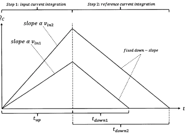
The Dual-Slope ADC
Figure 2-1 illustrates the dual-slope ADC, which is composed of an integrator, a
comparator and an input switch, Si. As shown in Figure 2-2, the dual-slope ADC
executes steps 1 and 2 sequentially to perform a conversion. The integration
ca-pacitor's voltage is initially at the comparator's threshold. In step 1, the integrator
integrates a current proportional to the input voltage for a fixed amount of time (tup). At the end of tup, an additional voltage (and charge) proportional to the input voltage
C Vint Sin R Vin Vref 0-0-+ Comp Vcomp
Figure 2-1: The Dual-Slope ADC
has been stored on the integration capacitor. Charge added in step 1:
Q1
= iintup = upIn step 2, the integration capacitor is discharged at a fixed rate set by the reference
voltage. The comparator flips after an additional duration of td,,n, when the added
charge from step 1 has been fully removed in step 2. Charge added in step 2:
Q
-Vref tdonQ2 = iref tdown - R
The more charge which has been added in step 1, the more time required to remove
that charge in step 2. This results in a measurement of vin:
Q1
+Q2=
0tdown
Vin = Vref t up
For a clocked system, rewriting t. = ntleock: ndown
Vin = -Vref no p
Step 1: input current integration Step 2: reference current integration I I
~II
?c
slope a
Vinslope a vn
Ifixed down - slope
t
tt
up tdownl
tdown2
several major disadvantages.
Firstly, the ADC's output is derived from the timing of a single, extremely precise
comparator decision, which places harsh requirements on the speed, accuracy and
noise performance of the comparator. This is because the ADC performs steps 1 and
2 sequentially, adding and then removing charge. At the end of step 1, substantial
charge - and high voltage - accumulates on the integrating capacitor. This is the
high tip of the triangle in Figure 2-2, which may be over 100V in precision designs.
This substantial instantaneous charge requires that the integration capacitor be an
expensive external component with a very low voltage coefficient, increasing the
bill-of-materials and circuit board area required to use the ADC.
The comparator requirements are relaxed if the integrator is allowing to swing over
a relatively large voltage, allowing for faster, more decisive comparator transitions.
Nevertheless, this requires a high supply voltage which is incompatible with modern, low-voltage manufacturing processes. For these reasons, the dual-slope ADC has
fallen out of mainstream use.
2.1.2
The Continuous Time EA ADC
Rin C Sin Vi n Vi nt Sud Rref +Vref/2 -Vref/2 0-Comp Vcomp
Figure 2-3: The CT EA ADC
The CT EA topology, illustrated in Figure 2-3, differs from the dual-slope by
performing steps 1 and 2 simultaneously. The ADC integrates a current proportional
decision is made to move the up-down switch, Sud to either +Ivref or -Vref. Over
the duration of that clock cycle, this either adds or subtracts a charge AQ = Vreftclck
This decision is made to drive the integrated charge towards zero; if Qjnt < 0, charge
is added, and if
Qine
> 0, charge is subtracted. The resulting (simplified) chargewaveform is shown in Figure 2-4 for a total of 10 clock cycles. The top dotted line
shows the total charge added by the input voltage (Qi) and the bottom dotted line
shows the total charge added by successive integrations of ±kVref (Q2). The solid
line is the sum of these two charges.
Qc
Step 1: integrated charge from vi,
--Q - - -- -
-1
t N
%' %
Step 2: known charge removed by ±vTf12 % OF e
tclock
Figure 2-4: Charge on CT EA ADC integration capacitor
Assuming that charge is added for nad cycles and charge is subtracted for nsubtract
cycles, the total charge contributed by step 2 is:
Vreftdcock
Q2 = &ei (nadd - nsubtract)
2Rref
Hence we can find vin as a function of nadd and nsubtract:
Vintclock
Q1
~ iintup (~~add+ nsubtractRin nsubtract - nadd
Vin ~~ Vref
2Rref subtract + nadd
In the example in Figure 2-4, with nadd= 4 and nsubtract = 6:
Rin 6 - 4 Vin = re 2 re 6 + 4f
As long as < the negative feedback action will always limit the
inte-grated charge to within
+(I|
l
+
IIre,
I
)tcloc. In other words, by performing steps
1 and 2 simultaneously (adding and subtracting charge simultaneously) we manage to drastically reduce the peak charge and voltage on the capacitor. This circumventsseveral problems with the dual-slope ADC: a small, on-chip integrating capacitor can
be used and the ADC can be implemented on a low-voltage manufacturing process.
Demands on comparator performance are greatly reduced, as the ADC output is no
longer derived from a single, precise comparator decision. Instead it is a result of
many decisions, one every clock cycle, where the comparator is triggered off of a
much larger, faster waveform.
Nevertheless, the CT EA ADC has a source of nonlinearity which compromises
its use for high-resolution conversion. Every clock cycle, Sed is set to either +"Vref
or - Vref. During each transition between +Vref and -jVref, charge is injected
from Sud into the integrating capacitor. As the number of switch transitions is unpre-dictable, this ill-defined number of charge injections appears as noise and nonlinearity
at the CT EA ADC's output[10]. High-resolution EA ADCs are still built in spite
of this effect, albeit with several engineering workarounds. These include the use
of bigger capacitors, higher integration currents and larger switches with carefully
balanced positive and negative charge injections. As these workarounds do not scale
well to a small, low-cost design, the following section will offer a method to lock the
2.2
Introducing the Landsburg ADC
2.2.1
Locking the Number of Switch Transitions
This section describes a return-to-zero method which fixes the number of switch
tran-sitions to improve the linearity of the CT EA ADC. If the number of switch trantran-sitions
(and hence the quantity of charge injection) is constant for each measurement, this
charge injection results in input offset instead of nonlinearity and noise. This
off-set can then be removed using zero-offoff-set calibration techniques, to be discussed in
Chapter 2.2.3.
VRref t tcl ock Varef +Vregf/2 t-V,,,r12
tclockFigure 2-5: Landsburg ADC 16-clock switching sequences: low (upper) &high (lower)
Previously, a decision was made to set Sud to +"Vref or -j1ore, at the start of
every clock cycle. Consider a system where this decision is made every 16 clock
cycles instead, and sets the
+.Ivref
or -jVref pattern for the next 16 cycles. In order2 2
to force
one +"Vref to -joref transition and one -"Vref to +'Vreyftransition, the
16-clock sequences in Figure 2-5 are used. The first cycle in each sequence is always
high and the last cycle in each sequence is always low, so one transition in each
direction must occur. As the charge from the first cycle cancels out the charge from
the last cycle, the high and low sequences add or subtract 14 cycles of charge from
the integrating capacitor. Hence, denoting the number of high and low sequences as
Nhigh and N1,, respectively, vi, can be found:
Q1
=iintup=
Vintclock 16(Nhigh+ Niow)
Rrn
Q2= Vreftdock 14(Nhigh -
Nio,)
2RrefQ1 + Q2 = 0
Rin 14(Nio, - Nhigh)
2Ref
16(Niow +
Nhgoh)Defining the total integration time, tintegration = tcdocknintegration = 16tcockNintegration,
where Nintegration = nintegration = Nhigh
+
Nio,:Rin 14(2Nio, - Nintegration)
Vin = Vref 2
Rref 16Nintegration
While this system has improved linearity over the CT EA ADC, it requires a much faster clock. If each 16-clock pattern represents one count, a clock with 16x frequency will be needed, compared to a CT EA ADC of equal resolution.
What if we define a single-clock charge difference to be one count, and we add an additional mechanism to measure single-clock charge differences? Then each 16-clock pattern represents 14 counts, and we only need a clock with 6 x frequency, compared to a CT EA ADC of equal resolution. The next section will explain how this is implemented in the Landsburg architecture.
2.2.2
Discerning One-Clock Charge Differences
Defining dont as the digital output code:
dout =
Ldout/14]
+ dout mod 14where we have only been able to discern the [dont/14] term. The remainder, dout mod 14
comes from the residual charge on the integrating capacitor at the end of the conver-sion, which should be in the range of ±142ef tdock. In order to measure this charge,
the Landsburg behaves like a 5-bit dual-slope converter. Figure 2-6 illustrates this
behavior for two example values of residual charge,
Qresiand
Qres2.In both cases,
after
nint16-cycle-sequence integration cycles,
Sinis opened to halt any further
cur-rent from vin and preserve the residual charge on the integrating capacitor.
Sudis
then set to -}Vref to integrate up for a fixed number of cycles
(nw,).
This ensuresthat
Q,
> 0 before the final down-integration. Finally, as in the dual-slope ADC, the
integration capacitor is discharged at a fixed rate (by setting
Sud to +-Vrej)until an
up-to-down comparator transition occurs. The number of clock cycles which elapse
before the comparator transition
(ndmv)indicate how much residual charge remained.
The entire conversion can be summarized with the formula:
(in
U14(2Naw - Nintegration) + nIown - nup)
re 2R,.e \ 16 Nintegration vin is disconnected, saving residual
GC
chargeQC
Qresl--- -Vnninn n nt nup ndown2Figure 2-6: Landsburg ADC residual charge measurement
The up-integration is always performed before the down-integration to ensure that the output is always measured on the up-to-down comparator transition. This elim-inates the effects of comparator hysteresis. This up-integration must be performed long enough to be certain that vint is above the comparator threshold before the
down-integration. Since the residual charge, Q.e on the integrating capacitor is in
the range of -14 to
+14
clock cycles of charge, it can be assumed that vit will be above the comparator threshold if you up-integrate for more than 14 clock cycles. Inother words, it is necessary for nu to be greater than 14. Similarly, ndow,,max must
be greater than (nup + 14) clock cycles to ensure that the up-to-down comparator
transition occurs.
The Landsburg ADC can be thought of as a split ADC. During the 'Measure
State', it acts as a first-order CT EA ADC with a fixed number of switch transitions
in order to find Ldout/14]. It then proceeds to the 'Residue State', where it behaves
like a dual-slope ADC to measure the remaining dut mod 14. One part of the system remains to be explained: the autozero mechanism.
2.2.3
The Autozero Mechanism
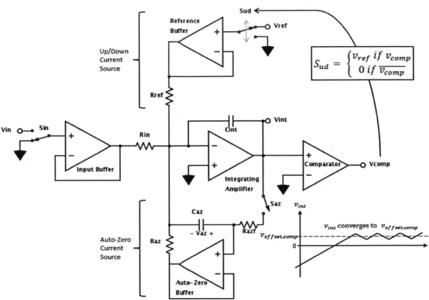
Up/Down Current Source Reference Sud Buffer +Vref Rref Sin Vin Rin Input Suffer Auto-Zero Current -Source Raz A 'I Clint movint + > Comparator Vcomp
Integrating
Amplifier Ca Saz aaz + az Auto-Zero BufferFigure 2-7 shows a block diagram of the Landsburg ADC. As in Figure 2-3, R, supplies the
Lu-
current which is integrated over nintegration = 16Nintegration clockRVre
cycles. In order to add or subtract the Rref current, the up-down switch (Sad) is
controlled to source a current of either 0 or Vref through Rref. The current through Rref
Raz is calibrated (by controlling the stored voltage on Caz) such that the combined
current into the integrating capacitor is Vi ± . This Raz current is nominally
- Vre but will adjust to provide additional current to null the effects of the main
offset sources in the circuit. These sources are as follows:
1. Integrating amplifier input offset voltage, Voffset,intamp
2. Integrating amplifier input bias current, ibias,intamp
3. Input buffer input offset voltage, Voffset,inamp
4. Auto-zero buffer input offset voltage, Voffset,AZamp
5. Reference buffer input offset voltage, Voffset,ref amp
6. Asymmetrical charge injection from up-down and down-up switching transitions 7. Comparator input offset voltage, Voffset,cwmp
The first six offset sources cause additional currents to flow into Cint. Sources 1-5
contribute additional currents of
V! f setmntamp Voffset,inamp Voffset,AZampand
RinJlRref IIRaz, I bias,intamp, Rin 7 Raz
Voffsetref amp respectively. The current from Source 6 is highly variable with switching
Rref
speeds and temperature. The first auto-zero mechanism (AZ1) uses a feedback loop
to store a precise voltage on Caz such that the current into Cit is * t +vref,. The
Rin 2Rref
second auto-zero mechanism (AZ2) ensures that Cint is charged to the comparator's transition voltage at the beginning of each measurement. This is essential as the comparator's transition voltage is Voffset,cmp above ground.
Figure 2-8 shows the ADC configuration during AZ1. Switches Sin and Sed are both set to simulate the conditions of a zero input voltage: Si, grounds the input, and Sud alternates between Vref and ground every 8 clock cycles. This creates a sequence which repeats every 16 clock cycles, containing one down-to-up transition and one up-to-down transition. As with a zero input signal, this waveform spends equal time integrating up as it does integrating down. Sa, is closed to form a feedback loop
Up/Down Current
-Source
Rref
Vin _ sin Rin
Input Buffer Auto-Zero Current -Source Raz Sud Reference VreT Buffer + -- r VSud V0, * in + Comparator Vcomp Integrating Amnplifier Saz Caz -az + Auto-Zero Buffer
Figure 2-8: Landsburg ADC when performing AZ
which servos the integration current (i.e. the current into Cit) to -
+
2± . Withthe grounded input buffer, the integration current should be ±
2R,,frefConsider the case where vaz = 0. With the switching waveform in Figure 2-5,
the integration current will be 0 or Rref Vref (in other words, 2Rref ref ± 2Rrefr
)
as well asthe currents caused by offset sources 1-5. The feedback loop thus has to set vaz such
that
iRz = -2 in addition to the currents from the offset sources. The resultantintegrating current is the desired t rf
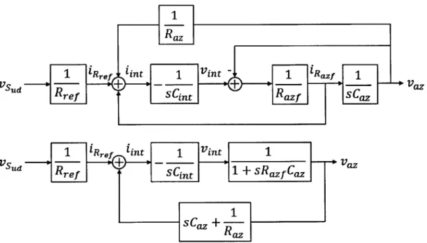
The feedback loop dynamics are illustrated in Figure 2-9. There is a 2nd-order
low-pass filter response from the switching voltage,
VS.dto the voltage stored on the
auto-zero capacitor, vz. This can be seen in the transfer function:
Vaz(S) _ Raz 1
Vsd(s) R,;
(
1
+
sRazCaz + sRazCint(l + sRazfCaz))VS.d is a square wave between 0 and Vref, of frequency 1 with a 50% duty cycle. It
Raz
1
LRreflint
V int
~ iRazfs
+
-- +--+Vazud
Rre
sCint
Raz
sCaz
,"LRre
int
V intV
~
R
0 - -s -+Vazsf Th
ref
sCint o
+
higazICaz
1
sCaz
+
Raz
Figure 2-9: Block diagram of AZ1 feedback loop, complete (upper) and simplified (lower)
}
Vref. The low-pass filter response filters out the high-frequency switching, allowingthe average voltage to be captured on the auto-zero capacitor. While the low loop
bandwidth is necessary to filter out the high-frequency switching, it mandates that
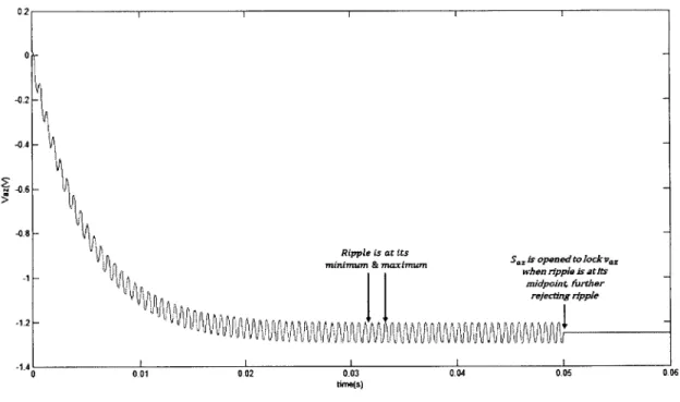
AZI must be run for a long period of time for vaz to converge to the full resolution of the ADC. A timing technique is used to further reject the high-frequency switching:
due to the 2nd-order low-pass filtering, high frequencies will have a known phase-shift
of 1800. Hence the opening of Saz (to sample & store Vaz onto Caz) can be timed to
the exact moment when the ripple is at its midpoint, to minimize the amount of
ripple which is sampled. This is shown in Figure 2-10.
To show that this feedback loop causes the integrating current to converge to
± 1' ,consider the circuit in Figure 2-8. During AZI, the integrating current is the
sum of currents from the up/down current source, the auto-zero current source and
offset sources 1-5. Any low-frequency component of the integrating current will not
be filtered out by the low-pass nature of the feedback loop, and will cause a shift in
Vaz. As a result, the loop will servo va, until there is no longer any low-frequency
0
-02
-046 -0.6 -1
-0.8
V Ripple is at its Sz oeed to occv,,
Rwhen ipple is atits
nidpoin4 further rejecing ripple -1.2 -14 0 0 01 002 0,03 0,04 0,05 0.06 time(s)
Figure 2-10: Ripple-rejection sampling of Vaz
square wave. During the Measure State, Saz is opened and S, is connected to V . This results in the integrating current becoming vin t ref, controlled by the position
of Sad.
It is necessary for this feedback loop to have low bandwidth in order to filter out the high-frequency switching. As a result, it takes a long time (50ms in the original design) for the loop to converge to the full resolution of the ADC.
The purpose of the second auto-zero mechanism, AZ2, is to compensate for the comparator's input offset voltage (offset source 6). As the comparator's transition voltage is the baseline for 'zero' charge stored on the integration capacitor, it is nec-essary to set vint to the comparator's transition voltage at the beginning of conversion. This is done with the circuit configured as in Figure 2-11. Due to the adjustment of
vaz in AZ1, the integration current is either 2Rref ref or - 2refvrf, depending on the position
of Sad. To move vint to the comparator's transition voltage, Sed is set to integrate
down if vpOM is high, and integrate up if vmOp is low. This creates the 'converge and dither' pattern for vint which can be seen in Figure 2-11. As long as AZ2 is run long enough for Vint to travel from the supply rails to the comparator transition voltage
Up/Down Current -Source VA Sin Vin + Rin Input Buffer Auto-Zero Current Source Rref Sud C Reference Buffer +
-
Eu
ref if lcompsd
0
if 17compI
Raz 11 0VintF
nt + Comparator Vcmp Integrating Amplifier I Caz Saz VnJaz + Vty., converges to vff,,,,
Auto- Zerr
Buffer
Figure 2-11: Landsburg ADC when performing AZ2
(Voffset,comp), Vint will
end up dithering around
the Voffset,comp bythe end of AZ2. A
change in polarity at the comparator's input will effect a change in integration current
between
- 2Rref refand
ref ,and the time delay of this change,
tdelay,AZ21o, affectsthe
2Rref
closeness with which Vof fset,com, dithers around vit. Neglecting noise, the following
upper bound can be placed upon this dithering:
Voffset,comp - Vint
I
dither < VreftdelayAZ21oot 2Rref Cint
2.2.4
Putting It All Together
A single conversion using the Landsburg ADC thus involves the following sequential
steps:
1. AZ1, to set
Vazand cancel out offset sources 1-5.
2. AZ2, to set Vint to the comparator threshold and cancel out offset source 6.
3. Measure State, to measure the output down to a 14 LSB resolution. (Chapter
2.2.1)
4. Residue State, to measure the mod 14 residue of the output and provide unit
clock resolution. (Chapter 2.2.2)
In the original Landsburg ADC described in [8], AZ1 was run for 50ms per
con-version, whereas the Measure State was run for 100ms to reject 50Hz and 60Hz noise.
AZ2 and the Residue State required a negligible duration of time. This gave the ADC
Chapter 3
System Design of the Modified
Landsburg ADC
This chapter describes various architectural changes made to the Landsburg ADC to
meet modern standards of ADC performance. Each change moves the design towards
being a fully-monolithic, high-resolution, single-supply ADC with pseudo-differential
inputs, implemented on a .25pum CMOS process. The target specifications of this
design are in Table 3.1.
Table 3.1: Target specifications for modified Landsburg ADC
Sample Rate 5 Samples/s
Resolution 19 bits
Power Consumption approximately 1.5mW
Supply Voltage 3V - 5V
Reference Voltage 1.25V 0 3V supply, 2.5V @ 5V supply
Input Offset <1 LSB
Gain Error <0.01% over temp
INL <1 LSB (<0.0002%) Full-Scale
3.1
Smaller Capacitors, Higher Resolution
The original Landsburg architecture has two large capacitors: the integrating capac-itor and auto-zero capaccapac-itor, each of which are on the order of dozens of nanofarads
[9]. These capacitors must be shrunk to a few hundred picofarads at most, so that
they can be placed on-die. Consider the voltage change at the output of the integrator as it integrates a constant current, I, for one clock cycle (the integrator has negative
gain):
Avint - tcdock
Cint
Reducing the capacitor size magnifies the voltage change. This is analogous to scaling up the entire Vint waveform, which will clip (causing a loss of linearity) as it is limited
by the supply voltage rails. In order to reduce the capacitance while staying within
the limits of the power supply, our options are to reduce the current and the length of each clock cycle (i.e. increase the clock frequency). There are other reasons for increasing the clock frequency. As the Landsburg ADC is an oversampling converter, its resolution increases linearly with clock frequency, so increasing clock frequency while keeping the Measure State time constant will increase the resolution of the converter.
3.1.1
Upper Limits on Resolution & Clock Frequency
What factors limit the clock frequency? Observe the main blocks of the Landsburg
ADC in Figure 2-7. Of these, the input buffer and auto-zero buffer are only required
to pass low-frequency signals. While the comparator's output must settle in less than one clock cycle, a fast-settling, low-power comparator can be built using a regenerative latching topology. The comparator's settling time is not the limiting factor on clock frequency.
In general, the most demanding and power-hungry parts of a system are those
which require both high bandwidth and high precision. In the Landsburg ADC,
these parts are the integrating amplifier and reference buffer. Consider the 16-clock return-to-zero sequences described in Chapter 2.2.1 and reproduced in the upper half
Available SettlingTime
1 clock up, 15 clocks dawn
Available SettlingTime
I I
2 clocks up, 14 clocks down
teack
Figure 3-1: Landsburg ADC
fled (lower)
Available SettlingTime
0. 1 1 11
L 15 clocks up, 1 clock down
tcla*k
Vet
0.
Available SettlingTime
JffiWI t
In- 14 clocks up, 2 clocks down
tclack
16-clock switching sequences: original (upper) &
modi-of Figure 3-1. The fastest transition which much be captured to full 19-bit accuracy
is the single high pulse in the low-sequence and the single low pulse in the
high-sequence. In other words, it is necessary for the integrating amplifier and reference
buffer to achieve >19-bit settling within a single clock cycle. The main constraint on
the maximum clock frequency (and maximum resolution) of the Landsburg ADC is
the full-resolution settling time of theses two components.
Fast, high-resolution settling requires the use of a high-bandwidth, high-gain,
dominant-pole amplifier. The limits of the manufacturing process will determine
the maximum achievable performance of this amplifier, which in turn defines the
maximum performance of the ADC. What can be done to extend the ADC's resolution
beyond this limit?
Consider the alternative set of 16-clock return-to-zero sequences in the lower half
of Figure 3-1. In the original set of sequences, every 16-clock sequence added or
subtracted 14 cycles of charge, as the first high pulse always negated the last low
pulse. In this new set, every 16-clock sequence adds or subtracts 12 cycles of charge,
as the first two high pulses always negate the last two low pulses. As described in
Chapter 2.2.2, the original Landsburg ADC's Measure State measures [dot/14J and
its Residue State measures dot mod 14. In this modified version, the Measure State
measures [dmt/12J and the Residue State measures dot mod 12. The overall gain
t
equation is now:
V Rin 12(2Nlo - Nintegration) + ndown - nup
Vi =Vref 2 re
- 16Nintegration
As each 16-clock sequence now causes a change of 12 (instead of 14) cycles of charge, we would need a clock which is 1- 12 = 116.7% the speed of an equal-resolution original
Landsburg ADC. However, the integrating amplifier and reference buffer now have 2 clock cycles to achieve >19-bit settling, and a correspondingly lower bandwidth. While the required clock speed has increased by 16.7%, the required bandwidth for these two circuit blocks has gone down to 11 = 58.3% of its original value. For a
given amplifier settling time, the ADC can now be run to a clock speed and resolution
which is 212 = 171.4% of its original limit.
We can generalize by saying that the return-to-zero sequences are m cycles long. Within each m-clock sequence, the first n cycles are always high and the last n cycles are always low. The original Landsburg then used m = 16 and n = 1, whereas the
modified Landsburg uses m = 16 and n = 2. In an ADC with R-bit resolution, the integrating amplifier and reference buffer are required to settle to over R-bit accuracy within ntdok time. Every m-clock sequence adds or subtracts (m - 2n)
cycles of charge. The range of possible outputs is 2R-1 counts above and below
ground, requiring the Measure State to run for (2 R-12n2) clocks. The generalized
gain equation is then:
Vin = in (n - 2n)(2N0 v - Nintegration) + ndown - nu)
vi =vr;2 Rref ( Nintegration
3.1.2
A Discussion of m and n
In order to optimi'ze our choice of m and n, we must consider their effect on the output swing of the integrating amplifier. As previously established, it is essential that its output does not clip in order to preserve linearity. Every m clock cycles, Snd is set such that Vint moves towards the comparator threshold (Voffset,comp) during the following m clock cycles.The largest possible voltage difference between vint and voffset,comp is
the furthest distance that vint can travel away from vo1fset,comp during those m clock
cycles. The upper and lower bounds on this voltage difference correspond to the minimum and maximum input current (iin), beyond which the ADC goes underrange or overrange.
What is the minimum and maximum input current? After AZI calibration, we
know the integration current, iint = R, ± Vf = iin + iu, where iud is the up/down
2Rref
current. If the input current is within bounds, this means that the average up/down current is of sufficient magnitude to overwhelm the input current and pull vint towards the comparator threshold. The most extreme average up/down currents are achieved if Sud performs just the 'high' sequence ((m - n) high pulses followed by n low pulses)
or just the 'low' sequence (n high pulses followed by (m - n) low pulses) for the
entire duration of the Measure State. Thus the two most extreme average up/down currents are 2Rre-f m-2n m and - 2Rref 'Vref ". It follows that the minimum and maximumm
input currents are just within -Vref 2R,ef m-2n m and 2Rref Vref m-2nm
Now we can finally calculate the maximum and minimum voltage difference be-tween vint and Voffset,comp. As the integrator has negative gain, the maximum
differ-ence is when iin = - 2Rref Vref m-2n m and Sud performs the 'low' sequence. vint starts just
be-low Vof1f set,comp, travels downwards for n cycles (integrating a current of -vref m- 2n+
2Rf) and then travels upwards for (m - n) clock cycles (integrating a current of
V-4 m-2n - e ). Calculating [Vint - Voffset,comp]max'
2Rref m nrf
[Vint - Voffset,comp]max = tdock Vref n(- m -2n+ 1) + (n - n)(- - 1))
Cint 2Rref M
[Vint - Voffset,comp]max tdk Vref 2 (in - 2n)
Cint 2Rref
Similarly, the minimum difference is when i Vref m-2n and Sud performs the 'high' sequence. vint starts just above Voffset,comp, travels downwards for (m - n)
cycles (integrating a current of Vrf m-2n + f,) and then travels upwards for n 2 ref m - 2 ref
clock cycles (integrating a current of 2Rrei m e- m.n
).
The lowest voltage in this 2RreiVint - Vof fset,compl min *
[Vint - Vof f set,comp] min - tdock Vref - 2 +
Cint 2Rref
m
- n)( M[Vint - Vo ffset,comp]min = -tdock 2Vref 2 (m - 2n +2n)
It can be seen that the magnitude of [vint - Voffset,comp]min is slightly greater than
[Vint - Voffset,comp]max. This asymmetry is because VS.d in Figure 3-1 always goes high
at the beginning of the sequence before going low, in other words, Vint starts moving downwards before moving upwards. This asymmetry can be reversed by switching the order of the m-clock sequences, by having the first n pulses always be low and the last n pulses always be high.
With all these equations, how do we choose m and n? n can range from 1 to m. While increasing n loosens the settling-time requirements for the integrating amplifier and reference buffer, it also increases the number of clock cycles required to perform a conversion, as does decreasing m. As 2n approaches m, the number of clock cycles approaches infinity. One approach is to start with n = 1 and increase n if the
amplifier settling times are just too slow for the target speed & resolution. Increasing
m decreases the number of clock cycles per conversion (allowing the use of a slower
clock) but also increases the required size of Cint to keep the integrator output swing from clipping. The eventual choice of m = 16 and n = 2 is a compromise between these effects.
3.1.3
Choosing Cint, Resolution & Clock Frequency
With m = 16, n = 2 and a total Measure State time of 0.1s (to reject 50Hz and 60Hz), we can calculate a need for at least (2R-1 m 2n) ~ 350000 clock cycles. With a
target resolution of 19 bits, this implies a clock frequency of >3.5MHz; 3.6MHz was chosen for redundancy. Ref = 200kQ and Cint = 50pF were also chosen. With a 2.5V reference, this results in a 0.84V to -0.85V integrator output swing around the
to -430mV. As described in Chapter 4.4, this fairly small voltage swing was chosen as it was not possible to build an integrating amplifier with rail-to-rail outputs which also met the gain, bandwidth and power requirements.
3.2
Single-Supply Operation & Eliminating the
Ref-erence Buffer
The original Landsburg design uses bipolar power supplies and a ground-referenced voltage reference. The switching voltage (controlled by Sad) varies between 0 and v,ef relative to the integrator's summing node, which is biased at ground. During AZI, the negative gain of the VSd to vaz transfer function causes vaz to servo to a voltage below the integrator's summing node.
From
Auto- Zero Buffer
Cint
Raz Vint
Rin
From
Input Buffer +-Comparator Vcomp Integrating vref Amplifier ) b) Rref2 Sud Rref Vref Vrel RefereceSud BRkference su r Vr: Vref
Buffer Vrr Sud Sjud
Rref Rref
L --- - ..-- ...-...--.
---Figure 3-2: Landsburg ADC single supply modifications, without reference buffer (b), with constant summing-node
with reference buffer (a), impedance (c)
upside-down. As shown in Figure 3-2a, the integrator summing node and comparator threshold are now biased at vref. As the amplifiers and comparator are powered from
ground to the positive rail (vdd), there is a voltage headroom of -Vref to (Vdd - Vref)
around the summing node. In this new configuration, the switching voltage now varies between -VTef and 0 relative to the integrator summing node. Vaz then servos
to a voltage above the integrator summing node.
In this new configuration, the summing node is now (Vref + Volfset,intamp) above
ground, where Voffset,intamp is the input offset of the integrating amplifier. Assuming that Voffset,intamp is small, Rref can simply be connected between the summing node
and ground to sink a (g
+
V"/" R-mP) reference current. A switch in series withRef allows this current to be turned on and off, as shown in Figure 3-2b. A double-throw switch is used to connect Rref to a basic Vref buffer when the reference current is not being sunk from the summing node. This ensures that Rref has consistent, code-independent self-heating, so that code-dependent temperature (and resistance) changes do not introduce non-linearity. The reference buffer is a fast-settling, high-gain, rail-to-rail amplifier. Its removal significantly reduces the cost of the Landsburg architecture.
In order to maintain consistent summing node impedance (and preserve linearity), an additional reference resistor (Rref2) is added, as shown in Figure 3-2c. This resistor is connected from Vref to the summing node when Rref is not connected. As this
resistor pulls very minimal current (Vfsetintamp), its matching to Ref is not critical.
In simulation, as much as 3% mismatch between Rref and Rref2 did not produce a
measurable increase in INL. This 'ff set intamp current also cancels out the vffsetintamp
Rref 2 Rref
term of the Rref reference current, removing the gain error caused by the integrating amplifier's input offset.
This description is incomplete because it assumes that there is no voltage drop across the switches. Taking switch resistance into account, the reference current through Rref will be less than vref and no longer ratiometric with Rin, increasing the ADC's gain drift over temperature. The next section describes a method to compensate for finite, nonlinear switch resistance.
3.2.1
Switch Resistance Compensation
Cint Vdd Vint V+ + -Vref/Rref Integrating Amplifier Dunmy Sud Switch Rref + VrefFigure 3-3: Simplified diagram of switch resistance compensation
As illustrated in Figure 3-3, switch resistance compensation is performed by using
a dummy switch to replicated the voltage drop across Suad. The intended current
through Ref is Rf, so a rough approximation of this current is made (using a resistor
and current mirror, not shown) and sourced into the dummy switch. Denoting the
voltage across the switch as Vswitch, we can describe the voltage at the integrating
amplifier's positive input:
V+in,intamp = Vref + Vswitch,dummy
Assuming the amplifier's inputs are at the same voltage:
V-in,intamp = V+in,intamp = Vref + Vswitch,dummy
V-in,intamp ~ i Re, Rref + Vswitch,Sud V Vref + Vswitch,dummy
The dummy switch and Sud are well-matched and in close thermal proximity. If they are carrying almost the same current, then Vswitch,Sud V Vswitch,dummy. This
the same current. Figure 3-5 shows a temperature sweep over 100 Monte Carlo simulations, comparing the current of the switch and resistor against just a resistor. With a 1.25V reference, the ±3u worst-case deviation from purely resistive behavior is 0.38ppm/0 C, producing a gain error of 0.006% over the entire operating temperature. The corresponding worst-case deviation using a 2.5V reference is 0.25ppm/0 C, or 0.004%. Both are within the <0.01% gain error target.
From Auto-Zero Buffer Ra Rin Rzi From Input Buffer Vref Sud JRr ef Cint SVint + Comparator Vcomp Vdd Integrating Vref V+ Amplifier ~Vref/Rref Sud V-4Rref2 Dummy Swih Vref
Figure 3-4: Implementation of switch resistance compensation
3.3
Pseudo-Differential Inputs & Auto-Zero
Consider the auto-zero mechanism illustrated in Figure 2-9. By using an up/down waveform with a 50% duty cycle during AZI, we are instructing the ADC to regard the ground voltage at the input buffer (as set by Si,) as the zero-point of the measure-ment, and store this information as a voltage across Caz. If we switch Sud between differential input pins vi,- and vi,_ instead of vir, and ground, the ADC is able to