Ministry of Higher Education and
Scientific Research
University of Akli mohand oulhadj -BOUIRA
Faculty of Sciences
Department of Physics
MEMORY
Presented for the diploma of :
MASTER
Field : Physique
domain : Materials Science
Option:
Physics of materials and nanomaterials
By
Ziane Hamza
Larbi Aissa
THEME
Title
Theoretical simulation and experimental investigation of the
structural properties of CdTe semiconductor using XRD.
In front of the jury composed of:
-
-
-
Firstly, we would like to express our sincere gratitude to
our advisor
Dr. Lazhar Boudjer
for advising us during the
realization of this work. A great thinks for his patience,
motivation, and immense knowledge.
We would also like to thank our committee members:
M.
Salime Benaiche
as a president of jury and
Dr Isam Hamma
as
an Examiner. In addition, we express a great respect to
administrative staff of department of Physics, and all teachers
of department of Physics.
Finely, we address a hot salutation to our colleagues in
two specialties of master: Physics of materials and theoretical
physics. In addition, we would like to think any person how
helped us during the realization of this work.
I. INTRODUCTION :... 3
II .The Techniques and applications of X-Rays. ... 3
II.1. Powder diffraction in general : ... 4
II.2. The Debye-Scherrer method : ... 5
II.3. The Guinier method ... 6
II.4. The Bragg-Brentano method ... 7
II.5. Laue method ... 8
II.5.1. Transmission Laue method – ... 8
II.5.2. Back reection Laue method ... 8
II.6. Ewald Sphere of Diffraction : ... 9
6.1 Ewald Construction : ... 10
III- You can use XRD to determine : ... 11
IV- Measurement of the Size of Crystal Grains and Heterogeneous Distortion : ... 11
IV-1 The grain size : ... 11
IV-2 Residual Stress and Strain : ... 12
V.THE DEFINITION OF MATERIAL : ... 13
V.1 PHYSICAL PROPERTY : ... 13
V.2 STATES OF MATERIAL : ... 13
V.2.1 GASES STATE : ... 14
V.2.2 LIQUIDS STATE : ... 14
V.2.3 SOLIDS STATE : ... 15
VI . The study of CdTe structure , crystallography and property : ... 18
VI.1 Introduction : ... 18
VI.2 The most important crystal structures : ... 19
VI.3Sphalerite structure : ... 19
VI.4 CdTe Crystalline Structure : ... 20
VII. Property of CdTe and structure band : ... 21
VII.1.4 p-n Junctions : ... 23
VII.2: Property of CdTe : ... 24
VII.2.1 ELECTRICAL PROPERTIES : ... 24
VII.2.2 Optical and electronic Properties of CdTe : ... 25
VII2.3 Chemical properties : ... 25
I-Study of the diffraction diagramme of the composed CdTe ... 26
I.1 Introduction : ... 26
I.2 Diffraction Intensities : ... 26
I.3 Miller Indices : ... 27
I.4-Structure Factor : ... 27
I.5 Multiplicity Factor : ... 27
I.6 The Polarization Factor : ... 28
I.7 The Lorentz-Polarization Factor : ... 29
I.8 Temperature Factor :... 30
I.9 Absorption Factor : ... 30
II The databases of a used powder diffractograms : ... 31
II.1The « PDF » Powder Diffraction File ... 31
II.1.1 Historic sight : ... 31
II.1.2 The different files of "PDF" : ... 33
II.1.3 Presentation of a printed map of the PDF file with "PCPDFWIN" (→ 2004 ) ... 33
II.1.4 The "COD" database (Crystallography Open Database) : ... 35
III-Calculation of diffraction patterns by the "CaRIne" software ... 35
III.1 INTRODUCTION : ... 36
III.2 Install procedure: ... 36
III.3 To run Setup : ... 36
III.4 For the cell definition : CdTe ... 37
III.5 To create the diamond unit cell, simply follow this sequence : ... 37
III.6 Conditions of Adding an atom : ... 38
III.7- Choosing the Atoms color Te: ... 39
III.8- Choosing the Atoms color Cd: ... 40
III.9-Forming The cell : ... 41
I.2 The structure factor of the composed CdTe is : ... 44
I.3 Calculation of Braggs angle : ... 45
II. Calculating the diagram with CaRine's software. ... 50
III. Structural study of the cdTe composed by X-ray diffraction ... 53
III.1 Comparison of diagrams: ... 55
III.2 By comparing the different intensities (Table VII), we note that: ... 56
III.3 Stress and Grain size ... 56
III.4 Calculation of grain size D and stress ε : ... 58
III.5Installation of the intensity in terms of 2θ ... 58
III.6 A comparison between PDF and EXP: ... 59
General
The discovery of X-ray diffraction by Max Von Laue in the last century was a truly important event in the history of science. Since then the use of X-ray diffraction has developed, it is now considered as one of the most powerful and flexible analytical technique for the identification and the quantitative determination of the crystalline phases of solids and powder samples.
The trend of this branch has accelerated particularly during the last decades due to several factors: the development of theoretical work on the structure materials, the construction of numerous sources of synchrotron radiation and neutrons as well as the development of new generations of surface detectors.
The utility of the powder diffraction method is one of the most essential tools in the structural characterization of materials has been proven both in academia than in the industrial field .
The powder diffraction method was invented in 1916 by Debye and Scherrer in Germany, and in 1917 by Hull in the United States. The technique has developed gradually, for more than half a century. It has been used for such as phase identification, precise measurement of crystal parameters or the analysis of structural imperfections from the diffraction line profile. The method was of great interest during the 1970s, following the introduction by Rietveld of the 6917 of a powerful method for the refinement of crystalline structures from a powder diagram. Initially applied to data from diffraction of neutrons, the method then extended to the field of X-ray diffraction. In a powder diffractogram the "diffraction lines" appear above a continuous background. They are characterized by three types of parameters" : line positions", and the "line intensity" parameters, and the "shape rays. "
If we want to simulate a theoretical diffractogram representative of a diffractogram experimental, it will be necessary to be able to reproduce this set of observations. It is in this last framework that the present work has been defined by highlighting the objectives .
the following :
• Calculation of the X-ray diffraction pattern (I = f (2θ)) of the compound of CdTe type
•Comparison of calculated diagrams with those of the database " Powder Diffraction File" of "JCPDS-ICDD" (Joint Committee on Powder Diffraction Standards-International Center of Diffraction Data).
•Comparison of calculated diagrams with diagrams computed by the software "CaRIne Crystallography 3.1" (Calculation and Representation of Crystalline Structures).
properties of CdTe compound, as well as structure band and Type doped CdTe ( both types P and n,and p n junctions ).
2-The second chapter is devoted to the description of the databases of powder diffractograms and calculation of diffraction pattern by software "CaRIne", Theoretical Study of the diffraction diagram of the composed CdTe.
3-The third brings together the results of the study of X-ray diffraction patterns CdTe compound and Calculation of grain size D and stress ε .
Chapter I
General information on X-ray
diffraction, powders and some properties
of CdTe compounds
I. INTRODUCTION
:
X-rays were discovered in 1895 by the German physicist Roentgen and were so named because their nature was unknown at the time. Unlike ordinary light, these rays were invisible, but they traveled in straight lines and affected photographic film in the same way as light. On the other hand, they were much more penetrating than light and could easily pass through the human body, wood, quite thick pieces of metal, and other "opaque" objects.[1]
It is not always necessary to understand a thing in order to use it, and x-rays were almost immediately put to use by physicians and, somewhat later, by engineers, who wished to study the internal structure of opaque objects. By placing a source of x rays on one side of the object and photographic film on the other, a shadow picture, or radiograph, could be made, the less dense portions of the object allowing a greater proportion of the x-radiation to pass through than the more dense. In this way the point of fracture in a broken bone or the position of a crack in a metal casting could be located.
Radiography was thus initiated without any precise understanding of the radiation used, because it was not until 1912 that the exact nature of x-rays was established. In that year the phenomenon of x-ray diffraction by crystals was discovered, and this discovery simultaneously proved the wave nature of x-rays and provided a new method for investigating the fine structure of matter. Although radiography is a very important tool in itself and has a wide field of applicability, it is ordinarily limited in the internal detail it can resolve, or disclose, to sizes of the order of 10-1 cm.
Diffraction, on the other hand, can indirectly reveal details of internal structure of the order of 10-8cm in size, and it is with this phenomenon, and its applications to metallurgical problems, that this thesis is concerned. The properties of x-rays and the internal structure of crystals are here Described.
II .The Techniques and applications of X-Rays.
The major technique used to derive the atomic structure of solids is the diffraction method. To obtain the most comprehensive information about a solid, other techniques besides may be used to complement a model based on diffraction data. These techniques include Scanning Electron Mcroscopy (SEM),Wavelength-Dispersive analysis of X-rays (WDX),Energy-Dispersive analysis of X-rays (EDX), Extended X-ray Atomic Fine Structure analysis (EXAFS) , Transmissionel Electron Microscopy (TEM), High Resolution
number of other methods For diffraction experiments, three types of radiation with a wavelength λ of the order of magnitude of inter atomic distances are used: X-rays, electrons, and neutrons. The shortest inter atomic distances in solids are a few times 10-10 m. Therefore the non-SI unit the angstrom 1Å=10-10
m is often used in crystallography. In the case of electrons and neutrons, their energies have to be converted to Broglie wavelengths. There are another techniques, among them we have:
II.1. Powder diffraction in general :
If we put a crystal in an X-ray beam we have to be a little bit lucky in order to observe any diffraction: The crystal has to be placed in the beam so as to fulfill the Bragg condition for diffraction. With a single-crystal diffractometer we can rotate the crystal in the beam about different axes and we can thereby always position any lattice plane correct for diffraction. Another approach to this problem is to put not one, but an infinite number of crystals into the beam. Thereby there will always be many crystals in the right position for diffraction from any of the lattice planes. This is the simple condition for powder diffraction. In practice we never have an infinite number of crystals, but it is essential for the method that we have enough crystals to fulfill the condition of always having many crystals in position for diffraction for each lattice plane. The process is best illustrated using an area detector: Each lattice plane will, according to Bragg’s law, scatter at a distinct 2θ-angle to the primary X-ray beam. If we position a crystal for diffraction and then rotate it about the primary beam it will still be in position for diffraction, and the diffraction spot will describe a circle with the primary beam as its center. With an ideal powdered sample we do not need to rotate the sample as there will always be lots of crystals in the correct orientation for diffraction from all lattice planes. The result will look like in Fig.II.1: A set of concentric rings, each representing a specific lattice plane.[2]
Due to the circularly symmetric pattern we do not need to collect the powder diffraction data with an area detector: It is sufficient to record the intensities on a line radially from the center and out. However, if our sample does not fulfill the conditions for an ideal powder sample the resulting rings may consist of distinct diffraction spots. In such a case an arbitrary radial line will not be representative for the powder sample. We can help the situation by spinning our sample during measurement and thereby improve the ―powder average‖. In some cases like when using high-pressure cells with very little sample, it may be necessary to record the full circles with an area detector and then integrate around the rings to
get the true powder diffract gram. For normal laboratory powder data collection it is essential that
Figure II-1 a simple powder diffraction experiment :
II.2. The Debye-Scherrer method :
The arrangement for the Debye-Scherrer method is shown schematically in Fig.II.2. The sample is loaded in a glass capillary, 0.1-0.5 mm in diameter, with a wall thickness of about 0.01 mm. The original method used a film strip for intensity recording. The film is placed all around the circle, which gives the diffraction pattern in the 2θ- range +180°. In the modern version, the film is replaced by a position sensitive detector covering 0 - 120°. The pattern can then be directly viewed on a monitor as it grows up. Most modern diffract meters are equipped with a focusing monochromator, which allow for the removal of the Kα2 radiation and on general gives sharper peaks.[2]
The advantage with Debye-Scherrer method is that it requires a very small amount of sample, from 50μg to a few mg depending on the size of the capillary. It is also convenient to handle air or moisture sensitive samples as the top of the capillary can be easily sealed. The data collection time can be made very short, it is often sufficient with a few minutes for phase identifications. When heavily absorbing samples are used, only a small part close to the capillary surface will contribute to the diffracted intensity. The data collection time will then have to be increased and the absorption will also cause some systematic peak position shifts (see below on Absorption effects). The background level is in general higher with this method as compared to for instance the Bragg-Brentano geometry due to scattering from air and the capillary.
Figure II. 2 : Debye-Scherrer method
II.3. The Guinier method
The geometry of the Guinier method is shown schematically in Fig. II.3. Its focusing monochromator makes it possible to remove the Kα2 line, so as to have pure Kα1 radiation. The sample is used in transmission mode and placed in a very thin layer on a plastic tape. Alternatively capillaries can be used as for the Debye-Scherrer method. Normally only a few hundred μg are used. The sample holder is kept spinning during data collection. Originally the powder pattern is recorded with a film strip placed around the focusing circle. The latest version uses an imaging plate strip and is equipped with an integrated readout system. The method has been and to some extent still is the work horse for phase identifications and unit cell determinations. As with the Debye-Scherrer geometry the background is relatively high due to air and tape scattering.[2]
II.4. The Bragg-Brentano method
The Bragg-Brentano geometry is the most commonly used geometry for powder diffractometers. It is schematically shown in Fig.II.4 in two 2θ-settings. In Fig.II.4 the source and the detector are each moved by an angle θ, while the sample is fixed horizontally. Alternatively the source is fixed and the sample is rotated by θ and the detector by 2θ. The sample is used in reflection mode and a comparably large amount of sample is needed, typically 0.5 cm3. Due to the large irradiated sample surface, the sample is not always rotated during data collection. The standard version uses filtered radiation and a monochromator in the diffracted beam. In this way fluorescence radiation is effectively removed, and in general the background level is very low. The secondary monochromator will not remove the Kα2 contribution and the peaks gradually split up in two at higher 2θ-angles. The Bragg-Brentano geometry is very good with medium to highly absorbing samples. Low sample absorption will allow the primary beam to penetrate the sample, causing profile broadening and asymmetry (see below on Absorption effects). Sample preparation is crucial for a good result. Uneven sample grinding may result in micro-absorption at the surface with strongly absorbing samples. It is often difficult to avoid preferred orientation when packing the sample in the sample hold.[2]
Figure II.4: Bragg’s representation of the diffraction condition as the reflection of X-rays by lattice planes (h k l).
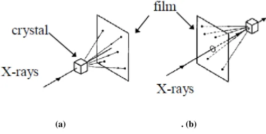
II.5. Laue method
Laue method was the first diffraction method used. A single crystal(fixed orientation) is required for this method. The technique use white radiation (range of wavelengths), typically unfiltered radiation from a X-ray tube. This falls on a single crystal that is fixed. Thus, the diffraction angle,θ, is fixed for every diffraction plane and for that particular θ value a certain wavelength will get diffracted, using equation λ = 2dsinθ. Thus, each diffracted beam will correspond to a certain wavelength which then falls on the film. Based on how the film is positioned there are two types in Laue method, as seen in figure II.5. [3]
II.5.1. Transmission Laue method :
The film is placed in the forward direction (behind the crystal) so that forward scattered radiation is detected. The film is at and perpendicular to the incident beam and the diffracted beams are partially transmitted through the sample before striking the film and hence the name.
II.5.2. Back reection Laue method:
- The film is placed between the incident beam and the crystal so that the back reected rays are used to form the image. The incident beam passes through a hole in the film and falls on the crystal.
(a) . (b)
Figure II-5 : (a) Transmission Laue method. (b) Back reection Laue method.Taken from Elements of X-ray diffraction - B.D. Cullity.
II.6. Ewald Sphere of Diffraction :
Diffraction, which mathematically corresponds to a Fourier transform, results in spots (reflections) at well-defined positions. Each set of parallel lattice planes is represented by spots which have a distance of 1/d (d: interplanar spacing) from the origin and which are perpendicular to the reflecting set of lattice plane. The two basic lattice planes (blue lines) of the two-dimensional rectangular lattice shown below are transformed into two sets of spots (blue). The diagonals of the basic lattice (green lines) have a smaller interplanar distance and therefore cause spots that are farther away from the origin than those of the basic lattice. The complete set of all possible reflections of a crystal constitutes its reciprocal lattice.[4]
The diffraction event can be described in reciprocal space by the Ewald sphere construction (figure below). A sphere with radius is drawn through the origin of the reciprocal lattice. Now, for each reciprocal lattice point that is located on the Ewald sphere of reflection, the Bragg condition is satisfied and diffraction arises. The Ewald sphere is a geometric construct used in electron, neutron, and X-ray crystallography which demonstrates the relationship between:
the wavelength of the incident and diffracted x-ray beams, the diffraction angle for a given reflection, the reciprocal lattice of the crystal It was conceived by Paul Peter Ewald, a German physicist and crystallographer. Ewald himself spoke of the sphere of reflection .Ewald's sphere can be used to find the maximum resolution available for a given x-ray wavelength and the unit cell dimensions. It is often simplified to the two-dimensional Ewald's circlemmodel or may be referred to as the Ewald sphere.
6.1 Ewald Construction :
A crystal can be described as a lattice of points of equal symmetry. The requirement for constructive interference in a diffraction experiment means that in momentum or reciprocal space the values of momentum transfer where constructive interference occurs also form a lattice (the reciprocal lattice). For example, the reciprocal lattice of a simple cubic real-space lattice is also a simple cubic structure. The aim of the Ewald sphere is to determine which lattice planes (represented by the grid points on the reciprocal lattice) will result in a diffracted signal for a given wavelength, , of incident radiation. The incident plane wave falling on the crystal has a wave vector Ki whose length is
. The diffracted plane wave has a wave vector Kf . If no energy is gained or lost in the di_raction process (it is elastic) then Kf has the same length as Ki. The difference between the wave-vectors of diffracted and incident wave is defined as scattering vector ΔK =Kf - Ki. Since Ki and Kf have the same length the scattering vector must lie on the surface of a sphere of radius . This sphere is called the Ewald sphere.
The reciprocal lattice points are the values of momentum transfer where the Bragg diffraction condition is satisfied and for diffraction to occur the scattering vector must be equal to a reciprocal lattice vector. Geometrically this means that if the origin of reciprocal space is placed at the tip of Ki then diffraction will occur only for reciprocal lattice points that lie on the surface of the Ewald sphere.
III- You can use XRD to determine :
• Phase Composition of a Sample
– Quantitative Phase Analysis: determine the relative amounts of phases in a mixture by referencing the relative peak intensities
• Unit cell lattice parameters and Bravais lattice symmetry – Index peak positions
– Lattice parameters can vary as a function of, and therefore give you information about, alloying, doping, solid solutions, strains, etc.
• Residual Strain (macrostrain) • Crystal Structure
– By Rietveld refinement of the entire diffraction pattern • Epitaxy/Texture/Orientation
• Crystallite Size and Microstrain – Indicated by peak broadening
– Other defects (stacking faults, etc.) can be measured by analysis of peak shapes and peak width
Among these uses we focus on structural properties )cell parameter, group of symmetry), the particle size and the strain application on it.[5]
IV- Measurement of the Size of Crystal Grains and
Heterogeneous Distortion :
IV-1 The grain size :
The grain size (D) was calculated using Debye-Scherrer formula from the full width at half maxima (FWHM).
Here, λ is the wavelength of source radiation, k is the Scherrer constant having a value 0.94, β2θ is the FWHM and θ is the Bragg’s angle.[6]
IV-2 Residual Stress and Strain
:Strain in a material can produce two types of diffraction effects. If the strain is uniform (either tensile or compressive) it is called macrostrain and the unit cell distances will become either larger or smaller resulting in a shift in the diffraction peaks in the pattern. Macrostrain causes the lattice parameters to change in a permanent (but possibly reversible) manner resulting in a peak shift. Macrostrains may be induced by heating of clay minerals. Microstrains are produced by a distribution of tensile and compressive forces resulting in a broadening of the diffraction peaks. In some cases, some peak asymmetry may be the result of microstrain. Microstress in crystallites may come from dislocations, vacancies, shear planes, etc; the effect will generally be a distribution of peaks around the unstressed peak location, and a crude broadening of the peak in the resultant pattern.[7]
Figure. IV.2 Change in peak profile, peak position, and its width
arising from lattice strain
V-THE DEFINITION OF MATERIAL :
All materials are composed of atoms.
- Atom:
Extremely small chemically indivisible particle , Atom is Greek for ―that which cannot be divided‖ There is so many different kinds of materials, which are organized by their composition and properties.
- Composition:
the types and amounts of atoms that make up a sample of material.
- Properties :
the characteristics that give each substance a unique identity
V.1 PHYSICAL PROPERTY :
Defined as - a characteristic that can be observed or measured without changing the identity or composition of the substance as ) the Colour , Odor, Taste , Size , Physical state (liquid, gas, or solid) , Boiling point, Melting point and Density )
V.2 STATES OF MATERIAL :
The Material can be classified according to its physical state and its composition •Physical State:
Solid Liquid Gas
•Classification into different states based upon:
Particle arrangement
Energy of particles
Distance between particles
Figure
V.2 : STATES OF MATERIAL
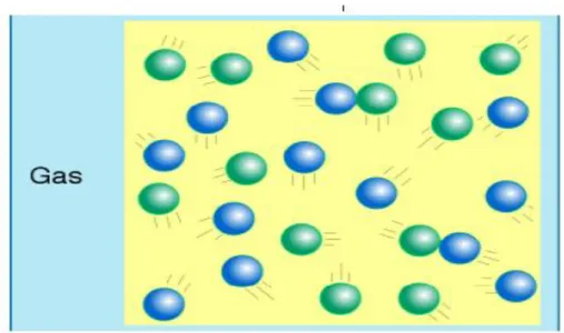
V.2.1 GASES STATE
:
Also known as vapor no fixed volume or shape, conforms to the volume and shape of its container atoms far apart i.e. low density and can be compressed moving at high speeds, colliding with container, moderate thermal expansion.
V.2.2 LIQUIDS STATE :
Has a definite volume, atoms are not widely separated, therefore high density and small compressibility- no definite shape i.e. follows the shape of its container
- Atoms move rapidly enough to slide over one another i.e. ability to flow - Small thermal expansion
V.2.3 SOLIDS STATE :
Has a definite shape and volume-True solids have very rigid, ordered structures, in fixed positions i.e. high density - atoms held tightly together, therefore incompressible
Figure V.2.3 : solid Materials
Based on the atomic arrangement in a substance, solids can be broadly classified as either crystalline or non-crystalline )amourph ( . In a crystalline solid, all the atoms are arranged in a periodic manner in all three dimensions where as in a non-crystalline solid the atomic arrangement is random or nonperiodic in nature. A crystalline solid can either be a single crystalline or a polycrystalline. In the case of single crystal the entire solid consists of only one crystal and hence, periodic arrangement of atoms continues throughout the entire material. A polycrystalline material is an aggregate of many
small crystals separated by well-defined grain boundaries and hence periodic arrangement of atoms is limited to small regions of the material called as grain boundaries as shown in FigV.2.3 The noncrystalline substances are also called as amorphous substances materials. Single crystalline materials exhibit long range as well as short range periodicities while long range periodicity is absent in case of poly-
crystalline materials and non-crystalline material.
Amorphous
solid
Crystalline solid
1 . The atoms or molecules of the
amorphous solids are not periodic in space .
2 . amorphous solids are isotropic i.e ,
the magnitude of physical properties are same along all directions of the solid .
3 . amorphous solids do not posses sharp
melting points .
4 . Breaks are not observed in the cooling
curve .
5 . When an amorphous solids breaks the
broken surface is irregular because it has no crystal planes .
1. The atoms or molecules of the
crystalline solids are periodic in space .
2. Some crystalline solids anisotropic .i.e,
the magnitude of physical properties ( such as refractive index , electrical conductivity , thermal conductivity , etc…. ) are different along different directions Of the crystal .
3. crystalline solids have sharp melting
points .
. Breaks are observed in the cooling
4
Curve of a crystalline solids.
5 . A crystal breaks along certain
crystallographic planes .
Figure V.2.3: two dimensional representation of single crystal , polycrystalline and non –crystalline materials
VI . The study of CdTe structure , crystallography and property :
VI.1 Introduction :
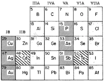
To introduce the papers that follow concerning specific properties and application of CdTe, this paper gives a comprehensive survey of the whole range of physical properties of this material.[8]
A number of these properties will be compared with those of the other IIB-VIA compounds ; although care has been taken to insure that the information presented for the other compounds is accurate, it should be noted that this information has been drawn primarily from published compilations of data, whereas for CdTe a systematic attempt was made to select the most reliable values from the current literature.
Most of the figures included are reproductions of figures from published papers. These have been chosen mainly because of their suitability as illustrations for a review article, and their selection does not imply any judgment concerning the overall merit of the papers in which they appear relative to other papers on the same subjects.
Figure VI -1: Portion of the periodic table including the elements of
VI.2 The most important crystal structures :
1-Sodium Chloride Structure Na+Cl- ) Rocksalt ( 2-Cesium Chloride Structure Cs+Cl-
3-Hexagonal Closed-Packed Structure ) wurtzite ( 4-Diamond Structure
5-Zinc Blende ) Sphalerite structure (
VI.3Sphalerite structure :
A conventional unit cell of the sphalerite (or zinc blende) structure is shown in Fig. 3. The structure has a face-centred cubic (fcc) Bravais lattice, with each lattice point populated by a basis comprising a Cd–Te pair; the separation between them being ¼ [111], i.e. ¼ of the body diagonal. An equivalent description is of two fcc sub-lattices, that for Cd being displaced from that for Te by a vector of ¼ [111]. The atom positions are the same as in diamond, but the Cd and Te sites are distributed over alternate
close-packed (i.e. {111}) planes.[9]
Figure VI.3 Conventional unit cell of the sphalerite structure. Cd sites at: 0, 0, 0 ½, ½, 0 ½, 0, ½ 0, ½,½ . Te sites at: ¼, ¼, ¼ 3/4, 3/4, ¼ 3/4, ¼, 3/4 ¼, 3/4, 3/4.
Zinc blende has equal numbers of zinc and sulfur ions distributed on a diamond lattice so that each has four of the opposite kind as nearest neighbors. This structure is an example of a lattice with a basis, which must so described both because of the geometrical position of the ions and because two types of ions occur. AgI, GaAs, GaSb, InAs , CdTe.
VI.4 CdTe Crystalline Structure :
CdTe has the cubic zincblende structure, the binary analog of the diamond structure. In this structure, the conventional cell is cubic and contains eight occupant atoms The following positions :
Cd : ) 0 0 0 ( ; ( ) ; ) 0 ( ; ) 0 (
Te : ) ( ; ) ; ) ; )
The unit of length being the cell parameter a .
Cadmium telluride (CdTe) is a crystalline compound formed from cadmium and tellurium. CdTe is used to make thin film solar cells, as an infrared optical material for optical windows and lenses, and also applied for electro-optic modulators. It has the greatest electro-optic coefficient of the linear electro-optic effect among II-VI compound crystals.
The crystal structure of CdTe is zincblende (cubic) as shown in figure 2.10. Its lattice constant is 0.648 nm at 300K and its thermal conductivity is 6.2 W·m/m2·K at 293 K. Bulk CdTe is transparent in the infrared, from close to its band gap energy (1.44 eV at 300 K, which corresponds to infrared wavelength of about 860 nm) out to wavelengths greater than 20 μm; correspondingly, CdTe is fluorescent at 790 nm. CdTe has very low solubility in water. It is a reducing agent and is unstable in air at high temperatures. Cadmium telluride is commercially available as a powder, or as crystals. It can be made into nanocrystals. [10]
FigureVI.4: structure ) Cadmium telluride ( CdTe
VII. Property of CdTe and structure band :
VII.1structure band :
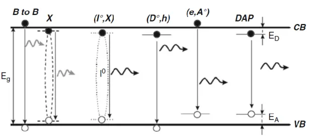
VII.1.1 Different radiative recombination processes :
A luminescence spectrum typically gathers a multitude of radiative recombination processes, as described in FigureVII.1.1 The near band edge emission region, corresponding to a luminescence spectrum in CdTe, can be divided into two main parts: one excitonic emission band, which can be attributed to X and (I, X) type radiative transitions, and one shallow emission band at lower energies, which corresponds to Donor-Accepter Pair (DAP) , (D, h), and (e, A) type radiative recombinations . [9]
The excitonic emission band brings a remarkable quasiparticle into play, namely the so-called exciton: an exciton consists in a free electron in the conduction band (CB) bound to a free hole in the valence band (VB) by coulombian interaction. Electrically neutral excitons form a mobile pair of opposite charge carriers, which is able to freely move in CdTe and thus act as a real probe of the crystalline quality
Below 1.56 eV in CdTe, radiative recombinations of free electrons in the CB to acceptors are referred to as (e, Å) type transitions in Figure VII.1.1
.
Figure VII.1.1 The different processes of radiative recombinations
VII.1.2 p-Type doped CdTe
:
Despite the p-type conductivity of undoped CdTe, the control of p-type doping is tricky due to its relatively high intrinsic resistivity. Typically, the dopants of the I and metal alkali groups were early used for the p-type .doping in CdTe, by substituting for Cd sites, and widely studied through the related optical properties. Nevertheless, their relative instability, which was evidenced through aging phenomena, constitutes a major obstacle for their efficient use. More recently, the dopants of the VI groups have been consequently more and more employed for the p-type doping in CdTe, by substituting for Te sites. [9]
VII.1.3 n-Type doped CdTe :
The control of n-type doping in CdTe is of great interest as regards the infrared detectors but is quite tricky to control due to the p-type conductivity of undoped CdTe and to the predominant role of VCd as compensating agent in Te-rich growth conditions. However, such compensation mechanisms are not always detrimental and even required concerning g- and X-ray detectors, in which a very high resistivity of up to 1010 Ω cm is expected to reduce their dark current. Consequently, PL spectra exhibit general features that are governed by the formation of defect complexes between VCd and the dopants, such as the so-called A centers for instance. Dopants of the III and VII groups are commonly employed for the n-type doping in CdTe, by substituting for Cd and Te sites, respectively.[9]
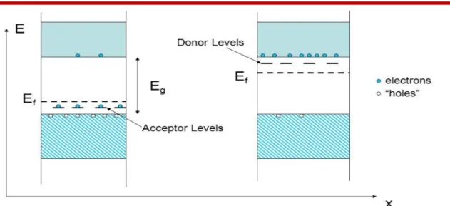
VII.1.4 p-n Junctions :
Junctions are formed when two materials are brought in intimate contact with each other. Homojunctions are formed when the two materials joined together are of the same type whereas two dissimilar materials on contact produce a heterojunction. There are a number of other ways in which junctions are classified. In most cases it is required to deposit metal over a semiconductor in order to form a contact.
A p-n junction, as the name indicates, is a junction formed between a p type and an n type material. p-n junctions are classified into: 1-Step junctions, and 2-Graded junctions.[10]
A step junction is one, which has uniform p doping on one side of a sharp junction and uniform n doping on the other side, whereas a graded junction is one, which has a graded impurity profile.
Before the n- and p-type materials are joined to form the junction, the n material has a large concentration of electrons and fewer holes and the converse is true for holes.
Figure VII.1.3 : Schema of diffrent semiconuctor types
( p-type ,and n –type)
FigureVII.1.4: Band Diagrams of p-type and n-type Semiconductors
)p-n Junctions
(VII.2: Property of CdTe :
VII.2.1 ELECTRICAL PROPERTIES
:
Technological applications of semiconductors depend on their electrical properties which will be reviewed here. The ability to extrinsically dope CdTe is crucial to most applications as well as sufficiently large carrier mobilities and diffusion lengths.[9]
VII.2.2 Optical and electronic Properties of CdTe :
As CdTe-based materials are direct bandgap semiconductors, belonging to the II-VI type group, the maximum of the valence band is located at same wave vector as the minimum of the conduction band. When photons of sufficient energies—typically higher than the bandgap energy in the case of photoluminescence (PL) measurements—, or when an electron beam—in the case of cathodoluminescence (CL) measurements—, encounter the CdTe surface, their absorption induces electronic excitations, from the ground state in the valence band to excited states in the conduction band. Subsequently, such electronic excitations are relaxed by the return of electrons to their ground state. If radiative relaxations proceed, photons with specific wavelengths are emitted from the CdTe surface and are characteristic of the energy levels in the bandgap. As such energy levels are directly related to the presence of native point defects, dopants, or even extended defects in CdTe, carrying out the study of such optical properties is of primary importance and opens the way to a real defect engineering. Its better understanding is essential for the control of the electronic and transport properties in optoelectronic devices.[9]
VII2.3 Chemical properties :
CdTe is insoluble in water. CdTe has a high melting point of 1041°C with evaporation starting at 1050°C. CdTe has a vapor pressure of zero at ambient temperatures. CdTe is more stable than its parent compounds cadmium and tellurium and most other Cd compounds, due to its high melting point and insolubility. Cadmium telluride is commercially available as a powder, or as crystals. It can be made into nanocrystals.[9]
Description of diffrenet technics were used
Chapter II
I-Study of the diffraction diagramme of the composed CdTe
I.1 Introduction :
In this chapter we present the results of the calculated diagramme in the diffraction of X – Ray ) I= f)2θ( ( : ) I : is the intensity of the bar , θ angle of Bragg ( of one composed CdTe.
This diagramme is calculated for the wave length of X – Ray : λcu = 1.54 Å ) anti-cathode of copper (.
We are interested in the following comparison between the calculated diagramme ,and the given diagramme form the basic data PDF ) powder diffraction file (.
And we calculate it witin the programme of CaRine .
I.2 Diffraction Intensities :
The integrated intensity, I (hkl) (peak area) of each powder diffraction peak with miller indices, hkl,is given by the following expression:
I (hkl) = |F|
2× M
hkl× LP(θ) ×TF(θ) × A(θ)……) 1 (
Where :
h k l : Miller Indices |F|2= Structure Factor
Mhkl= Multiplicity
LP(θ) = Lorentz and Polarization factors
TF(θ) = Temperature Factor (more correctly referred to as the displacement parameter) A(θ) = Absorption Factor
This does not include effects that can sometimes by problematic such as preferred orientation and extinction.[13]
I.3 Miller Indices :
Miller Indices are a symbolic vector representation for the orientation of an atomic plane in a crystal lattice and are defined as the reciprocals of the fractional intercepts which the plane makes with the crystallographic axes.[13]
I.4-Structure Factor :
The structure factor reflects the interference between atoms in the unit cell. All of the information regarding where the atoms are located in the unit cell is contained in the structure factor. The structure factor is given by the following summation over all atoms in the unit cell.[13]
F
)hkl(= ∑
)j(
exp [2 ….. )2(
I.5 Multiplicity Factor :
In a powder diffraction experiment the d-spacings for related reflections are often equivalent. Consider the examples below:
Cubic –(100), (010), (001), (-100), (0-10), (00-1) → Equivalent Multiplicity Factor = 6 –(110), (-110), (1-10), (-1-10), (101), (-101), (10-1), (-10-1), (011), (0-11), (01-1), (0-1-1) → Equivalent Multiplicity Factor = 12
In general for a cubic system where the Miller indices are n1, n2 and n3 (all unequal) the multiplicity factors Mhkl are:
n100 (i.e. 100) → M = 6 n1n1n1 (ie 111) → M = 8 n1n10 (i.e. 110) → M = 12 n1n20 (ie 210) → M = 24 n1n1n2 (i.e. 221) → M = 24 n1n2n3 (ie 321) → M = 48
The multiplicities are lower in lower symmetry systems. For example in a tetragonal crystal the (100) is equivalent with the (010), (-100) and (0-10), but not with the (001) and the (00-1). [13]
Table I : Multiplicity Factor
.I.6 The Polarization Factor :
The polarization factor p arises from the fact that an electron does not scatter along its direction of vibration . [13]
In other directions electrons radiate with an intensity proportional to (sin α)2:
00l :6 hhh : 8 0kk : 12 0kl : 24 hhl : 24 hkl : 48 Cubique 00l :2 0k0 :6 hh0 :6 hk0 :12 0kl :12 hhl :12 hkl :24 Hexagonal et rhomboédrique 00l :2 0k0 :4 hh0 :4 hk0 :8 0kl :8 hhl :8 hkl :16 Quadratique 00l :2 0k0 :2 h00 :2 hk0 :4 h0l :4 0kl :4 hkl :8 Orthorhombique 0k0 :2 h0l :2 hkl :4 Monoclinique hkl :2 Triclinique
The polarization factor (assuming that the incident beam is unpolarized):
P )
𝛉 (
…………...… )3(
I.7 The Lorentz-Polarization Factor :
The Lorenz factor L depends on the measurement used technic, and for the diffractometer data obtained by the usual θ-2θ or ω-2θ scans, it can be written as :
L =
=
……… ) 4 (
The combination of geometric corrections are lumped together into a single Lorentz-polarization (LP )θ ( ) factor:
LP )
𝛉 (
………... ) 5 (
The effect of the LP factor is to decrease the intensity at an intermediate angles, and increase the intensity in the forward and backwards directions , as it was explained in the previous figure.
I.8 Temperature Factor :
As is well known, atoms in a crystal is not kept at fixed points, they are rather moving around their mean positions by thermal vibration and the amplitude of such vibration increases with increasing temperature .[13]
Figure
.I.8 : The fraction of the diffracted intensity contributed from a
surface layer of depth t to the total diffracted intensity of a sample of
semi-infinite thickness.
I.9 Absorption Factor :
According to Beer’s law, absorption reduces the intensity of an X-ray beam travelling through a given material by an amount which depends on the material and the length of the path travelled by the radiation in it.The intensity of the diffracted X-rays is reduced due to absorption by the factor : [14]
I /I
0= e−
ux
………. ) 6 (
Here x is the total path length and μ is the linear absorption coefficient of the crystal
I α F
hklF
*
hkl
= F
hkl2
II The databases of a used powder diffractograms :
II.1The « PDF » Powder Diffraction File
II.1.1 Historic sight :
In the late 1930s, a meeting was held on Gibson Island, Maryland Wheeler P. Davey of Pennsylvania State College to discuss the creation of a file X-ray diffraction chemical analysis. In 1936, Hanawalt and Rinn published a Work on the interest of powder diffractograms for the qualitative analysis of mixtures. In 1941 the Joint Committee on Chemical Analysis was created by X-Ray Diffraction Methods from the American society for Testing Materials "(A.S.T.M). The British Institute of Physics publishes 1000 diffractograms Of format maps (3×5). The diffractograms are essentially derived from "Pennsylvania State University "and headquarters is in Philadelphia, Pennsylvania,seat of the A.S.T.M.[11]
In 1969, the previous association was transformed into a "non-profit organization" under the Name of "Joint Commitment on Powder Diffraction Standards (J.C.P.D.S) " . In 1978, to take account of the international contribution, besides U.S.A., to the constitution of the file, The International Center of Diffraction Data (I.C.D.D.) was added. Acronym Therefore, is "J.C.P.D.S.-I.C.D.D. "This" International Center "is based in Newtown Square (Pennsylvania, U.S.A.) .
Table II.: History of the "PDF"
Year Event 1941 Publication of the first ASTM files .
1962 The cards are inserted into a computer .
1965 The indexes are edited from the computer file .
1969 The various companies that joined the ASTM founded the JCPDS .
1976 Beginning of the project of setting up computer data base.
1978 First version of the computer database .
1979 The JCPDS becomes the ICDD .
1985 Extension of data format (additional information) with PDF-2 format .
1987 Abandonment of distribution in the form of cards .
1998 Integration of a calculated forms from the ICSD (Inorganic crystal Structure database) of the FIZ (informatios file zentrum, Karlsruhe) .
2002 Integration of the cards calculated from the structure database of the National Institute of Standards and Technology (NIST)
Creation of the PDF-4 format: the forms are put in a relational database (Microsoft Access) .
Integration of CCDC's Cambridge structure database (Cambridge Crystallographic data center) in the PDF-4 / Organics database
2004 Abandonment of PDF-1.
2005 2005
Integration of a calculatedforms from the Linus Pauling File structure base (LPF)
The relational database format becomes Sybase; PDF-2 also becomes a Relational database .
After the paper supports (individual cards, books), microfiches, tapes and floppy disksThe year 1987 saw the advent of the CD-ROM and the opening up of In the use of P.D.F. Currently, the "J.C.P.D.S.-I.C.D.D." Distributes on CDROM The following files: P.D.F.-2 and P.D.F.-4 + (inorganic compounds and some Basic organic compounds), P.D.F.-4 / Mineral (mineral compounds), P.D.F.-4 / Organics (Organic compounds).
II.1.3 Presentation of a printed map of the PDF file with "PCPDFWIN" (→ 2004 )
The most comprehensive database at the moment is the Powder Diffraction File (PDF) of "JCPDS - ICDD" (Joint Committee on Powder Diff Center of Diffracion Data) [16] . PCPDFWIN is a software for searching and sorting files from the PDF database Up-to-date and distributed by the ICDD. This database contains diffraction diagrams Of the X-rays by single-phase powders. Figure II.1.3.shows an example of the card 27-1402 of silicon.
The file number (an additional file is added per year) which is obtained by subtracting 1950 of the number of the year under consideration (example: the 1994 file number is 44). - track the number of the card in the file (in the order of recording in the file,Up to 2500).
Zone 2: Chemical formula and name (in the IUPAC nomenclature).
Zone 3: Essentially: "structural formula" and mineralogical name (nomenclature of
( " International Mineralogical Association "
Zone 4: Experimental conditions for recording
Zone 5: Crystallographic data (A = a / b, C = c / b, Z = number of form groups By grid),
density, reference of the publication of the diffractogram and factor of Smith and Snyder (Smith and Snyder Figure Of Merit: SS / FOM) On some maps between 5 and 6: Optical data.
Zone 6: General comments .
Zone 7: Symbol of "quality" of the diffractogram.
The 5 used symbols:
Symbol "*": all the lines are indexed and very good quality of analysis (d, I)
(Δ2θ | ≤ 0.03 °).
Symbol "i": not more than 2 non-indexed lines, | Δ2θ | ≤ 0.06 °, quantitative
measurements of I.
No symbol: indexed (sometimes not completely) but of poor quality (does not respond Criteria for "*" or "i").
Symbol "O": not indexed and of average quality (low precision, or mixture of phases,
or Bad chemical characterization, etc.) .
Symbol "C": diffractograms Calculated from atomic positions. At the beginning these cards Have been added in the case of known crystal structures but of diffractograms Of poor quality experimental powders.
Sometimes finds additional abbreviations: b (wide, diffuse), n (unauthorized indices By the given space group), + (other possible indices), ...
II.1.4 The "COD" database (Crystallography Open Database) :
In 2003, an international group of crystallographers proposed to create a new Data that they call COD (Crystallography Open Database).
The principle Is that researchers who determine new crystal structures feed this base By simply sending the CIF file via the Internet. Calculations of derived data may then be Including the simulation of powder diffractograms for the purpose of analysis qualitative.
In 2007, the P2D2 database (Predicted Powder Diffraction Database) Contained ~ 61,000 records. In 2011 it had more than 150,000.
software
III.1 INTRODUCTION :
CaRIne Crystallography software was developed since 1989 and is used by thousands of persons around the world for teaching, research and edition. It is now available in a totally rethought version. The first part of this new version 4.0 is focused on 3D modelisation of cells, crystals, surfaces, grain boundaries and interfaces.
The new 4.0 version has an architecture and a graphic user interface which will, later on, allow an easy and very powerful integration (multi-tasks) of the simulation and analysis modules such as: stereographic projections, X-Ray diffraction on powders and singlecrystals, reciprocical lattices in 3D and 2D, a dedicated module of electronic diffraction, but also a good assistance in writing out reports.[12]
As long as these modules will not be available, the 3.0 version will be delivered with the 4.0 version.
The different files of both versions (3.0 and 4.0) are of course compatibles. The authors, Cyrille Boudias and Daniel Monceau Those different functions are usually divided in several software. CaRIne brings them together in a friendly interface. This is time and cost saving. Moreover CaRIne displays in a clear way the relations which exist between the different representations which is all the most appreciated among the teaching world.
CaRIne is curently used in 30 countries by more than 1500 teams and laboratories for research and teaching in the physics and chemistry and materials science fields.
III.2 Install procedure:
The Setup program provided by CaRIne Crystallography performs all tasks necessary for installing the CaRIne components. You can install everything at once or install just a subset and upgrade it later with additional libraries, samples, help files, or other components.
III.3 To run Setup :
1. Place Disk 1 in drive A (or B...) or CD-ROM.
2. From the control panel select Add/Remove programs menu and type A:\Setup in the command line box.
3. Install prompts you with a dialog box that describes the program and lets you continue or exit.
When the installation procedure is ended, Setup add CaRIne 3.0 in the Start Menu :
III.4 For the cell definition : CdTe
The diamond unit cell .The Tellurium cell consists of a FCC cell with an atom of Tellurium )Cd( at (0,0,0) and with four additional atoms of cadmium )Te (on the tetrahedral sites.
coordinates of these atoms are : the Z Y X 1/4 1/4 1/4 atom : 1 1/4 3/4 3/4 atom :2 3/4 1/4 4 / 3 atom:3 3/4 3/4 1/4 atom:4
III.5 To create the diamond unit cell, simply follow this sequence :
1 ـــ New from the Files Menu, a new window appears,
2ــ Cubic - Face-Centred from the Cells Menu, enter 6.481Å . 3ــ choose the Tellurium )Te( atom from the Mendeleev's table.
4ــ Creation from the Cells Menu, add the four atoms of cadmium )Cd (on tetrahedral sites, when this is done, you should obtain the following :
This function enables an atom to be added, particularly in an interstitial position. The following steps should be taken :
1. it is advisable to display the frame (a,b,c) or (x,y,z) (this helps to find one's bearing within the lattice).
2. as adding an atom is relative to a full site, select an atom close to the interstitial site, with the mouse.
3. enter the coordinates of the vector included between the selected atom and the new atom you would like to add.
.
- We click on the Mendeleev's table , another table will show up ,then we click on Te , finally we click on OK.
Access to Mendeleev's table Colour of atom (click on to
access to colour palette)
Add a new position
Figure III-6.1 :The information entering window
Figure III.6.2 Periodic Table.
Selected element Te Periodic table Reduced coordinates Paramètres de maill
III.7- Choosing the Atoms color Te:
-We click on color,and the window will show up below. After that we choose the appropriate color. Finally, we click on OK.
Figure III-7.1 : The Colors Of Te
-Adding the coordinates of Te.
Figure III-7.2: The coordinates of
Te
finally we click on OK.
III.8- Choosing the Atoms color Cd:
We click on color,and the window will show up below. After that we choose the appropriate color. Finally we click on OK
Figure III.7.3 : Periodic Table.
Figure III.8 .
: The Colors Of Cd
1
Figure III.8.2: The coordinates of cd
III.9-Forming The cell :
At the end ,the cell CdTe shows up. After that we click on OK.
Figure III-11 : CaRine's spectre of the composed CdTe
Figure III.10 the method of drowing the spectre CdTe.
In this investigation, we used the BRUKER- AXSD8 diffractometer with wave length RX λcu= 1.54 Å and graphite filter (fig IV-12 )
The sample was scanned at ambient temperature in the angular range of 20° – 110° of 2θ with the scan rate of 0.001 ° /s.
Chapter III
Resultes and discussion
I. The study of the diagramme diffraction of thecomposetCdTe :
I.1 Calculation and discussion of the structure factor :
The composed CdTe is crystallized in the diamond cubic structure The position of Te and Cd in the cell are :
Cd:
) 0 0 0 ( ; (
) ; )
0 ( ; ) 0
(
Te : )
( ; )
; )
; )
I.2 The structure factor of the composed CdTe is :
Calculated in relation with () so 2
Fhkl = fTe. (1 + ( )+ ( )+ ( )( + fCd.( ( )+ ( )+ ( )+ ( )( FhKL = fTe .( + fCd .( FhKL = fTe .( + fCd .( FhKL = ( (fTe + fCd ) ΙFhKLΙ2 = 16 (fTe2 + fCd2 +2 fTe fCd ) ΙFhKLΙ2 = 16 (fTe2 + fCd2 +2 fTe fCd cos /2(h+k+l )) ……….. )8 (
we disting wish four cases : ΙFhKLΙ2 = 16 (fTe2 + fCd2 )
when (h+k+l) is odd ……….... )8- 1 ( ΙFhKLΙ2 = 16 (fTe + fCd )
when (h+k+l) is an even multiple two 2(2n) ……. . ...)8 – 2 ( ΙFhKLΙ2 = 16 (fTe - fCd )2
when (h+k+l) is an odd multiple two 2(2n +1) …….... ...) 8 – 3 ( ΙFhKLΙ2 = 0 when (h+k+l) is mixed………..………... ) 8 – 4 (
We suppose N = h2 + k2 + l2, N is a whole number
After the conditions ) 8-1(, ) 8-2 and )8-3 ( the planes )hkl( which diffracts according ( to the bidding possible values are in the following table
I
Table I : the diffracted composed plans of the type CdTe
I.3 Calculation of Braggs angle :
The parameters of the cubic cell of the given composed CdTe from the database ) PDF ( . a = 6.841 Å
We have to calculate angles of diffraction using the relation of Bragge.
Sin )θ ( =
……….
) 9 (
N
)
hkl)
3
(1 1 1)
4
(2 0 0)
8
(2 2 0)
11
(3 1 1)
12
(2 2 2)
16
(4 0 0)
19
(3 3 1)
20
(4 2 0)
24
(4 2 2)
27
(3 3 3)
27
(5 1 1)
32
(4 4 0)
35
(5 3 1)
36
(6 0 0)
The inter reticulaire distance dhkl in the cubic structure and given within the following
relation
d
hkl=
√
………… ) 10 (
-The angles of the calculated diffraction for the wave length RX λcu= 1.54 Å of the composed CdTe are in the table II
Θ(°) dhkl √ (hkl) 11.76 0.205 3.741 1.732 (1 1 1) 1 13.74 0.237 3.240 2 (2 0 0) 2 19.63 0.336 2.291 8 2882 (2 2 0) 3 23.20 0.394 1.954 38316 (3 1 1) 4 24.3 0.411 1.870 38464 (2 2 2) 5 28.37 0.475 1.620 4 (4 0 0) 6 31.18 0.517 1.486 48358 (3 3 1) 7 32.09 0.531 1.449 48472 (4 2 0) 8 35.59 0.582 1.322 48898 (4 2 2) 9 38.12 0.617 1.247 58196 (3 3 3) 10 38.12 0.617 1.247 58196 (5 1 1) 11 42.22 0.672 1.145 58656 (4 4 0) 12 44.65 0.702 1.095 58916 (5 3 1) 13 45.46 0.712 1.080 6 (6 0 0) 14 58.09 0.848 0.907 7.141 ( 5 5 1) 15
table II : diffracted angles of the composed CdTe for the wavelength
λ
cu= 1.54 Å
The values of the atomic diffusion factor of Te and Cd . According to sinθ / λcu )λcu= 1.54 Å ( sinθ / λcu
f
Tef
Cd0.129
46.193
43.104
0.154
44.515
41.624
0.218
40.419
37.746
0.255
38.163
35.440
0.267
37.632
34.884
0.308
35.584
32.730
0.336
34.131
31.210
0.345
33.663
30.725
0.377
32.299
29.338
0.400
31.424
28.468
0.400
31.424
28.468
0.436
29.753
26.865
0.456
28.155
26.129
0.462
28.959
26.129
Table III : The values of the atomic diffusion factor of Te and Cd .
according to sinθ / λ
cu)λ
cu= 1.54 Å
(
The values of Lorentz-polarization's factors, the multiplicity ,the factor structure ,and the intensities of the bars in the diffraction of the composed CdTe are in the following table IV.
Table IV: the calculated values of Lorentz-polarisation's factors, the
multiplicity ,the factor stracture and intensities.
(h K L) 2 ( ) LP( ) mhkl F 2 hkl Ihkl Irel (% ) 1 (1 1 1) 23.53 23.07 8 63867.96 12045172.76 100 2 (2 0 0) 27.49 16.294 6 133.726 17431.46 0.1 3 (2 2 0) 39.27 7.521 12 97756.27 8822699.38 77.83 4 (3 1 1) 46.41 5.17 24 43398.53 5384889. 47.50 5 (2 2 2) 48.60 4.656 8 120.824 4500.45 0.03 6 (4 0 0) 56.74 3.273 6 74668.84 1466346.71 12.93 7 (3 3 1) 62.37 2.64 24 34223.82 2168421.75 19.13 8 (4 2 0) 64.19 2.48 24 138.109 8220.27 0.07 9 (4 2 2) 71.18 2 24 60785.91 2917723.98 25.74 10 (3 3 3) 76.24 1.76 8 28766.316 405029.74 3.36 11 (5 1 1) 76.24 1.76 24 28766.316 1215089.18 10.08 12 (4 4 0) 84.45 1.509 12 51289.566 929366.95 7.71 13 (5 3 1) 89.31 1.42 48 24341.57 1659121.62 13.77 14 (6 0 0) 90.93 1.40 6 128.14 1076.36 0.008
After calculating , and from the table IV we designed the following diagram in figure I using ( origin 8 program ).
Figure I: Diagrame of the X –RAY calculated of composed CdTe
(λ=1.54Å)
II. Calculating the diagram with CaRine's software
.
We have calculated the X - ray diffraction patterns of the composed CdTe by the "CaRIne" software for the wavelengths λCu = 1.54Å .
The table VI represents the deduced values which are represented in figure II (CaRine'sspectre of the composed CdTe ) .
(h K L)
2θ ( )
I
hkl(1 1 1)
23.76
100
(2 0 0)
27.50
0.1
(2 2 0)
39.29
74.5
(3 1 1)
46.43
44.2
(2 2 2)
48.63
0
(4 0 0)
56.77
11.2
(3 3 1)
62.40
16.2
(4 2 0)
64.22
0.1
(4 2 2)
71.22
20.4
(3 3 3)
76.28
10.8
(5 1 1)
76.28
10.8
(4 4 0)
84.49
5.9
(5 3 1)
89.36
10.2
(6 0 0)
90.96
0.0
Table VI: Results of calculation of the X-ray diffraction pattern of the
composed CdTe. (λcu = 1.54Å) obtained by the "CaRIne" softwar
The international diagrame PDF ( data base ) of the composed CdTe ( Cadmium Telluride ) under-λcu = 1.54Å wave length , and 150770 reference .
The table represent the deduced values wtich are represented in figure III ( from