HAL Id: cea-02952505
https://hal-cea.archives-ouvertes.fr/cea-02952505
Submitted on 29 Sep 2020
HAL is a multi-disciplinary open access archive for the deposit and dissemination of sci-entific research documents, whether they are pub-lished or not. The documents may come from
L’archive ouverte pluridisciplinaire HAL, est destinée au dépôt et à la diffusion de documents scientifiques de niveau recherche, publiés ou non, émanant des établissements d’enseignement et de
Advanced light management based on periodic textures
for Cu(In,Ga)Se_2 thin-film solar cells
Chidozie Onwudinanti, Robin Vismara, Olindo Isabella, Louis Grenet, Fabrice
Emieux, Miro Zeman
To cite this version:
Chidozie Onwudinanti, Robin Vismara, Olindo Isabella, Louis Grenet, Fabrice Emieux, et
al.. Advanced light management based on periodic textures for Cu(In,Ga)Se_2 thin-film solar
cells. Optics Express, Optical Society of America - OSA Publishing, 2016, 24 (6), pp.A693.
Advanced light management based on periodic
textures for Cu(In,Ga)Se2 thin-film solar cells
Chidozie Onwudinanti,1 Robin Vismara,1* Olindo Isabella,1 Louis Grenet,2 Fabrice
Emieux,2 and Miro Zeman1
1Delft University of Technology, Photovoltaic Material and Devices, Mekelweg 4, 2628CD Delft, The Netherlands 2Commissariat a l’Energie Atomique, Laboratoire d’Innovation pur les Technologies des Energies Nouvelles et les
nanomatériaux, 17 rue des Martyrs, 38054 Grenoble Cedex 9, France
Abstract: We have used 3-D optical modelling to investigate light
management concepts based on periodic textures and material optimization for photovoltaic devices based on Cu(In,Ga)Se2 (CIGS) absorber material.
At first, calibration of the software based on the characterization of a reference (1500-nm thick) CIGS device was carried out. The effects of 1-D and 2-D symmetric gratings on the cell were then investigated, showing significant improvement in anti-reflection effect and in absorptance in the active layer, achieved by excitation of guided modes in the absorber. In addition, device configurations endowed with alternative back reflector and front transparent conductive oxide (TCO) were tested with the goal to quench parasitic absorption losses at front and back side. The use of In2O3:H (IOH) as front and back TCO, combined with an optimized 2-D
grating structure, led to a 25% increase of the optical performance with respect to an equally-thick flat device. Most of the performance increase was kept when the absorber thickness was reduced from 1500 nm to 600 nm.
©2016 Optical Society of America
OCIS codes: (050.1950) Diffraction gratings; (310.6860) Thin films, optical properties;
(350.6050) Solar energy.
References and links
1. P. Jackson, D. Hariskos, R. Wuerz, O. Kiowski, A. Bauer, T. M. Friedlmeier, and M. Powalla, “Properties of Cu(In,Ga)Se2 solar cells with new record efficiencies up to 21.7%,” Phys. Status Solidi Rapid Res. Lett. 9(1), 28–31 (2015).
2. P. Jackson, D. Hariskos, R. Wuerz, W. Wischmann, and M. Powalla, “Compositional investigation of potassium doped Cu(In,Ga)Se2 solar cells with efficiencies up to 20.8%,” Phys. Status Solidi Rapid Res. Lett. 8(3), 219– 222 (2014).
3. A. Chirilă, P. Reinhard, F. Pianezzi, P. Bloesch, A. R. Uhl, C. Fella, L. Kranz, D. Keller, C. Gretener, H. Hagendorfer, D. Jaeger, R. Erni, S. Nishiwaki, S. Buecheler, and A. N. Tiwari, “Potassium-induced surface modification of Cu(In,Ga)Se2 thin films for high-efficiency solar cells,” Nat. Mater. 12(12), 1107–1111 (2013). 4. M. Gloeckler and J. R. Sites, “Potential of submicrometer thickness Cu(In,Ga)Se2 solar cells,” J. Appl. Phys.
98(10), 103703 (2005).
5. C. van Lare, G. Yin, A. Polman, and M. Schmid, “Light coupling and trapping in ultrathin Cu(In,Ga)Se2 solar cells using dielectric scattering patterns,” ACS Nano 9(10), 9603–9613 (2015).
6. Z. Yu, A. Raman, and S. Fan, “Fundamental limit of light trapping in grating structures,” Opt. Express 18(S3 Suppl 3), A366–A380 (2010).
7. E. Yablonovitch, “Statistical ray optics,” J. Opt. Soc. Am. 72(7), 899–907 (1982).
8. J. Malmström, O. Lundberg, and L. Stolt, “Potential for light trapping in Cu(In,Ga)Se2 solar cells,” in 3rd World
Conference on Photovoltaic Energy Conversion, K. Kurokawa, ed. (2003), pp. 344–347.
9. A. Čampa, J. Krč, J. Malmström, M. Edoff, F. Smole, and M. Topič, “The potential of textured front ZnO and flat TCO/metal back contact to improve optical absorption in thin Cu(In,Ga)Se2 solar cells,” Thin Solid Films
515(15), 5968–5972 (2007).
10. M. Schmid, R. Klenk, M. Ch. Lux-Steiner, M. Topič, and J. Krč, “Modeling plasmonic scattering combined with thin-film optics,” Nanotechnology 22(2), 025204 (2011).
11. L. C. Andreani, P. A. Kowalczewski, C. I. Mura, M. Patrini, M. Acciarri, S. Binetti, A. Sassella, and S. Marchionna, “Towards CIGS slar cells with reduced film thickness: a study of optical properties and of photonic structures for light trapping,” in 27th European Photovoltaic Solar Energy Conference and Exhibition (2012), p. 2334.
12. M. Schmid, J. Klaer, R. Klenk, M. Topič, and J. Krč, “Stability of plasmonic metal nanoparticles integrated in the back contact of ultra-thin Cu(In,Ga)Se2 solar cells,” Thin Solid Films 527, 308–313 (2013).
13. C. Colin, I. Massiot, A. Cattoni, N. Vandamme, C. Dupuis, N. Bardou, I. Gerard, N. Naghavi, J.-F. Guillemoles, J.-L. Pelouard, and S. Collin, “Broadband light-trapping in ultra-thin nano-structured solar cells,” Proc. SPIE
8620, 86200C (2013).
14. M. Xu, A. J. H. Wachters, J. van Deelen, M. C. D. Mourad, and P. J. P. Buskens, “A study on the optics of copper indium gallium (di)selenide (CIGS) solar cells with ultra-thin absorber layers,” Opt. Express 22(52), A425–A437 (2014).
15. ANSYS white paper, “ANSYS HFSS,”
http://www.ansys.com/Products/Simulation+Technology/Electronics/Signal+Integrity/ANSYS+HFSS. 16. O. Isabella, S. Solntsev, D. Caratelli, and M. Zeman, “3-D optical modeling of thin-film silicon solar cells on
diffraction gratings,” Prog. Photovolt. Res. Appl. 21(1), 94–108 (2013).
17. M. Zeman, O. Isabella, S. Solntsev, and K. Jäger, “Modelling of thin-film silicon solar cells,” Sol. Energy Mater. Sol. Cells 119, 94–111 (2013).
18. O. Isabella, H. Sai, M. Kondo, and M. Zeman, “Full-wave optoelectrical modeling of optimized flattened light-scattering substrate for high efficiency thin-film silicon solar cells,” Prog. Photovolt. Res. Appl. 22(6), 671–689 (2014).
19. NREL, “Reference solar spectral irradiance: air mass 1.5,” http://rredc.nrel.gov/solar/spectra/am1.5/. 20. C. Roger, S. Noël, O. Sicardy, P. Faucherand, L. Grenet, N. Karst, H. Fournier, F. Roux, F. Ducroquet, A.
Brioude, and S. Perraud, “Characteristics of molybdenum bilayer back contacts for Cu(In,Ga)Se2 solar cells on Ti foils,” Thin Solid Films 548, 608–616 (2013).
21. NT-MDT white paper, “NTEGRA Spectra,” http://www.ntmdt.com/afm-raman/ntegra-spectra.
22. J. A. Sap, O. Isabella, K. Jäger, and M. Zeman, “Extraction of optical properties of flat and surface-textured transparent conductive oxide films in a broad wavelength range,” Thin Solid Films 520(3), 1096–1101 (2011). 23. Perkin Elmer white paper, “LAMBDA 950 UV/Vis/NIR Spectrophotometer,”
http://www.perkinelmer.com/Catalog/Product/ID/L950.
24. P. A. van Nijnatten, “An automated directional reflectance/transmittance analyser for coating analysis,” Thin Solid Films 442(1–2), 74–79 (2003).
25. J.A. Woollam Co, white paper, “M-2000 Ellipsometer,” http://www.jawoollam.com/m2000_home.html. 26. J.A. Woolam Co, white paper, “CompleteEASE,” http://www.jawoollam.com/completeease.html.
27. T. Hara, T. Maekawa, S. Minoura, Y. Sago, S. Niki, and H. Fujiwara, “Quantitative assessment of optical gain and loss in submicron-textured Cu(In1−x Gax)Se2 solar cells fabricated by three-stage coevaporation,” Phys. Rev. Appl. 2(3), 034012 (2014).
28. K. Söderström, J. Escarré, O. Cubero, F.-J. Haug, S. Perregaux, and C. Ballif, “UV-nano-imprint lithography technique for the replication of back reflectors for n-i-p thin film silicon solar cells,” Prog. Photovolt. Res. Appl.
19(2), 202–210 (2011).
29. R. Vismara, Optical Characterization of Photovoltaic Materials and Structures for Thin-Film Solar Cells Based
on Advanced Texturization (Delft University of Technology, 2014).
30. K. Jäger, D. N. P. Linssen, O. Isabella, and M. Zeman, “Ambiguities in optical simulations of nanotextured thin-film solar cells using the finite-element method,” Opt. Express 23(19), A1060–A1071 (2015).
31. H. Tan, E. Psomadaki, O. Isabella, M. Fischer, P. Babal, R. Vasudevan, M. Zeman, and A. H. M. Smets, “Micro- textures for efficient light trapping and improved electrical performance in thin-film nanocrystalline silicon solar cells,” Appl. Phys. Lett. 103(17), 173905 (2013).
32. H. Sai, K. Saito, and M. Kondo, “Enhanced photocurrent and conversion efficiency in thin-film microcrystalline silicon solar cells using periodically textured back reflectors with hexagonal dimple arrays,” Appl. Phys. Lett.
101(17), 173901 (2012).
33. M. L. Brongersma, Y. Cui, and S. Fan, “Light management for photovoltaics using high-index nanostructures,” Nat. Mater. 13(5), 451–460 (2014).
34. K. Orgassa, H. W. Schock, and J. H. Werner, “Alternative back contact materials for thin-film Cu(In,Ga)Se2 solar cells,” Thin Solid Films 431–432, 387–391 (2003).
35. W. N. Shafarman and J. E. Phillips, “Direct current-voltage measurements of the Mo/CuInSe2 contact on operating solar cells,” in Photovoltaic Specialists Conference (IEEE, 1996), pp.917–919.
36. T. Wada, N. Kohara, T. Negami, and M. Nishitani, “Chemical and structural characterization of
Cu(In,Ga)Se2/Mo interface in Cu(In,Ga)Se2 solar cells,” Jpn. J. Appl. Phys. 35(Part 2, No. 10A), L1253–L1256 (1996).
37. J. Springer, A. Poruba, L. Müllerova, M. Vanecek, O. Kluth, and B. Rech, “Absorption loss at nanorough silver back reflector of thin-film silicon solar cells,” J. Appl. Phys. 95(3), 1427–1429 (2004).
38. Z. C. Holman, S. De Wolf, and C. Ballif, “Improving metal reflectors by suppressing surface plamson polaritons:
a priori calculation of the internal reflectance of a solar cell,” Light Sci. Appl. 2(10), e106 (2013).
39. R. Santbergen, H. Tan, M. Zeman, and A. H. M. Smets, “Enhancing the driving field for plasmonic nanoparticles in thin-film solar cells,” Opt. Express 22(S4 Suppl 4), A1023–A1028 (2014).
40. S. Krishnakumar and C. S. Menon, “Electrical and optical properties of molybdenum trioxide thin films,” Bull. Mater. Sci. 16(3), 187–191 (1993).
41. H. Fujiwara and M. Kondo, “Effects of carrier concentration on the dielectric function of ZnO:Ga and In2O3 studied by spectroscopic ellipsometry: Analysis of free-carrier and band-edge absorption,” Phys. Rev. B 71(7), 075109 (2005).
42. T. Koida, H. Fujiwara, and M. Kondo, “Hydrogen-doped In2O3 as high-mobility transparent conductive oxide,” Jpn. J. Appl. Phys. 46(28), L685–L687 (2007).
43. D. J. L. Brémaud, Investigation and Development of CIGS Solar Cells on Flexible Substrates and with
Alternative Electrical Back Contacts (ETH Zurich, 2009).
44. T. Koida, H. Fujiwara, and M. Kondo, “Reduction of optical loss in hydrogenated amorphous silicon/crystalline silicon heterojunction solar cells by high-mobility hydrogen-doped In2O3 transparent conductive oxide,” Appl. Phys. Express 1, 041501 (2008).
45. K. Kushiya, “CIS-based thin-film PV technology in solar frontier K.K,” Sol. Energy Mater. Sol. Cells 122, 309– 313 (2014).
46. T. Koida, Y. Kamikawa-Shimizu, A. Yamada, H. Shibata, and S. Niki, “Cu(In,Ga)Se2 solar cells with amorphous oxide semiconducting buffer layers,” IEEE J. Photovolt. 5(3), 956–961 (2015).
1. Introduction
Cu(In,Ga)Se2 (CIGS) is a prominent absorber material in thin-film solar cells technology,
having demonstrated efficiencies up to 21.7% [1]. Highly performing devices have an absorber 2.5 to 3-μm thick [1–3]. Due to indium scarcity, however, reduction of the absorber thickness is of great importance. In fact, cell-manufacturing costs could be decreased while increasing further the diffusion of this technology in the photovoltaic (PV) market. On the other hand, a reduction of the absorber thickness has significant drawbacks, in particular increased recombination at the back contact and significant decrease of light absorption [4,5]. Absorptivity of the thin absorber can be increased by using textured interfaces, either random or periodic, to achieve light trapping. Recently [6], studies have shown that periodic gratings can increase the absorptance of a layer beyond the 4n2 theoretical limit (i.e. the Yablonovitch
limit), which is calculated for randomly textured interfaces [7]. While extensive research has been carried out on light trapping for thin-film silicon solar cells, only a handful of papers on light management in CIGS devices has been published so far [4,5,8–14].
In this contribution an analysis of the optical performance of CIGS solar cells with periodically structured interfaces is presented. The effect of the gratings geometrical dimensions was investigated to find the optimal dimensions. A study of the propagation of light inside the device was also carried out, to observe which optical phenomena take place when periodic gratings are employed. Finally, cell configurations with different materials were examined with the goal to reduce optical losses inside CIGS devices.
2. Experimental method
The performance of different device configurations shown in this work was analyzed by means of optical modelling. The Ansoft® High Frequency Structure Simulator software (HFSS) [15] was employed. This is a three-dimensional (3-D) Maxwell equations solver based on the Finite Element Method (FEM), which allows for the design and simulation of thin-film solar cells having arbitrarily complex 3-D structures [16–18], so-called models.
In all simulations perpendicular incidence of light was assumed; the optical performance of different models was evaluated by computing the total cell reflectance (R) and the absorptance in each layer (Ai) forming the model. Total reflectance was calculated in terms of
S-parameters as R = |S11|2 [16]. The absorptance of the i-th layer was calculated as the
integral, over the layer volume Vi, of the square of the magnitude of the electric field E:
2 0 1 ( ) Im( ) 2 i i i V A λ = ε ε ω
E dV (1)where λ is the wavelength of light in vacuum, ε0 is the dielectric constant of vacuum, εi is the
(complex) relative permittivity of the i-th material, and ω is the angular frequency. Due to the presence of a metallic back reflector transmittance is numerically negligible, therefore the law of conservation of energy can be written as R + Ai = 1, which was always verified in our
simulations. The implied photocurrent density Jph-i generated (in the active layer) or lost (in
the i-th supporting layer) could be computed by convoluting the absorptance Ai and the
1400 nm ph-300 nm ( ) ( ) ( ) i i J λ = −q
A λ Φ λ λd (2)where q represents the elementary charge. Note that this implied photocurrent density represents an approximation of the performance of a real device, and does not take into account electrical processes which have a significant influence on the cell’s photocurrent density. Further details on the modelling process can be found in reference [16].
The reference cell, provided by Commissariat à l’énergie atomique et aux énergies
alternatives (CEA – Alternative Energies and Atomic Energy Commission), is a typical CIGS
device. The solar cell is composed (from bottom to top) of a molybdenum (Mo) back reflector (500 nm) sputtered on a soda lime glass substrate; a CIGS absorber (~1500 nm); a cadmium sulphide (CdS) buffer layer (50 nm); an intrinsic zinc oxide (ZnO) layer (50 nm); and an aluminum-doped zinc oxide (ZnO:Al, AZO) front transparent conductive oxide (TCO, ~400 nm) A detailed description of the cell manufacturing process and the composition of the CIGS layer can be found in the work by Roger et al. [20]. The optical performance of the device was characterized by external quantum efficiency (EQE) and reflectance measurements.
In order to create a representative model of the real device, a thorough physical and optical characterization was performed. The device was subjected to cross-sectional scanning electron microscope (SEM) imaging to examine the layers and determine their thickness. The surface morphology of the various layers was studied using atomic force microscopy (AFM) on the NT-MDT Ntegra Spectra [21]. The refractive index of materials composing the CIGS solar cell was determined using spectrophotometry for the ZnO:Al layer [22], and spectroscopic ellipsometry for all other layers. Spectrophotometry was carried out on the Lambda950 spectrometer [23], with the Automated Reflectance/Transmittance Analyzer (ARTA) [24]. For all but the CdS layer, the spectroscopic ellipsometry was performed on the M-2000 spectroscopic ellipsometer by J.A. Woollam Co. controlled by the CompleteEASE software [25,26]. The optical constants for CdS were supplied by Center for Innovative Photovoltaic Systems (CIPS) of Gifu University in Japan [27].
3. Results
3.1. Cell characterization & software calibration
To ensure that simulation results are a good approximation of the behavior of real devices, calibration of the software is necessary. To this purpose, the reference device provided by CEA was modelled in HFSS. Simulation results were then compared with reflectance and EQE measurements of the reference solar cell.
Fig. 1. (a) SEM cross-section of the reference cell (with indication of measured external parameters) and (b) surface morphology of the CIGS layer (from AFM).
In order to make the model as similar as possible to the real device, its correct characterization is of paramount importance. AFM was used to characterize the surface morphology of the CIGS surface, depicted in Fig. 1(b). From the measurement a series of statistical parameters was extracted, most importantly the average dimensions of the surface morphological features: average feature height (hf = 215 nm) and width (or generalized
correlation length, LCG = 185 nm [28]). These parameters are important to correctly model the
surface morphology of the absorber layer.
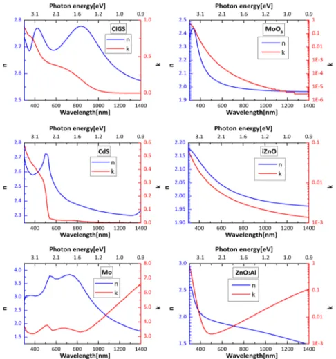
Fig. 2. Wavelength-dependent real part (n) and imaginary part (k, extinction coefficient) of the refractive index of all materials used.
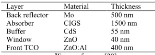
On the other hand, the thickness of each layer of the device was estimated from the SEM image shown in Fig. 1(a). A summary is presented in Table 1. These values are fairly typical for CIGS devices, with the exception of the absorber layer (1500 nm). This value is much smaller than state-of-the-art (2500-3000 nm) CIGS devices [1–3] but, in exchange of a reduction in photogenerated current, allows for a substantial decrease of material utilization. Along with the geometry of the individual layers, the optical constants of the materials involved play the most important role in the accuracy of the simulations. High-resolution wavelength-dependent complex refractive index data for each material are required. Figure 2 shows the optical constants acquired and used in this work.
According to the results of the AFM scan, a model with an irregular, pseudorandom texture on the CIGS surface was prepared with the correct thickness of each layer from SEM cross-section analysis. A 3-D rendering is displayed on the left side of Fig. 3. The pseudorandom texture was devised as follows: using a (pseudo)random number generator in MATLAB©, a series of random numbers whose average was equal to the correlation length
(LCG) of features on the CIGS surface was generated. A similar set was created for the average
feature height (hf). These sets were then combined to yield a pseudorandom set of truncated
dimensions (hf and LCG) yielded by the AFM scan of the reference cell. Alternative
elementary feature shapes such as tetrahedra, hemispheres, and triangular pyramids were tested, as well as craters. However, these other shapes provided no clear discernible benefit and are less simply applicable in a 3-D design. The CdS and intrinsic ZnO layers were constructed to be conformal to this texture on the CIGS, given their small thickness (~50 nm). On the other hand, the ZnO:Al layer was built to have features smoothened compared to the ones on the CIGS surface, given the relatively large thickness of the layer (~400 nm). Observations of the SEM cross-section depicted in Fig. 1(a) confirm that the roughness of the cell front surface is significantly lower than the one of CIGS. The molybdenum layer, meanwhile, was modelled with regular nano-features (~30 nm), determined from both observation of the SEM cross section and reports of similar analysis in literature [27].
Table 1. Estimated thickness of device layers.α
Layer Material Thickness Back reflector Mo 500 nm Absorber CIGS 1500 nm Buffer CdS 55 nm Window ZnO 40 nm Front TCO ZnO:Al 400 nm
αFrom reference [29].
The pseudorandom approach was preferred to the modelling of texture with regular (periodic) features in order to correctly model the scattering effect of the CIGS random texture (opposed to the diffraction of light which takes place in case of periodic structures). A perfectly random structure can be defined as a grating with an infinite period P (i.e. same pattern is never repeated). On the other hand, simulations can be significantly quicker and less computationally demanding if the simulated domain is as small as possible, and then repeated an infinite amount of times by means of (periodic) boundary conditions. A study by Jäger et
al. showed that for relatively small features sizes, similar to those deployed in our study for
modelling the CIGS front surface, a unit cell width of 3 x LCG is sufficient to closely
approximate the randomness of larger areas [30]. A similar preliminary analysis conducted for this work showed that the minimal unit cell size required was 4 x LCG. Larger unit cells were
modelled and simulated, but did not show significant improvements in accuracy.
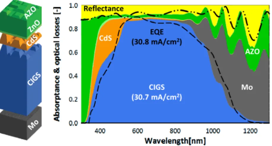
The calibration results are shown in Fig. 3 on the right side, where the simulated and measured characteristics are compared. Each colored area in the plot represents the absorptance in the corresponding layer identified in the 3-D sketch of the model. Absorption in the CIGS (blue area) well corresponds to the measured EQE (dashed black line) except in two portion of the spectrum:
• Between 350 nm and 450 the simulated absorptance is higher than the measured EQE. Since the simulations do not include electrical effects like recombination (i.e. they assume 100% collection efficiency) EQE is expected to be lower than simulated absorption.
• Between 950 nm and 1150 nm measured EQE is higher than the simulated absorptance. In this spectral area it appears that the reflectivity of molybdenum is underestimated (i.e. the absorptance in the molybdenum layer is overestimated).
Over the whole simulated spectrum, the average difference between simulations and measurements is 0.038, a value in line with similar studies carried out by other groups (0.028 [9], 0.027 [27]). It must be noted, however, that the work by Čampa et al. [9] as well as that by Hara et al. [27] employ 1-D simulators, while this contribution employs a rigorous 3-D Maxwell equations solver. The integration of both simulated CIGS absorptance and measured EQE with the photon flux of AM1.5 spectrum as in Eq. (2) yields very similar photocurrent density values: 30.7 mA/cm2 (simulation) and 30.8 mA/cm2 (measurement).
Fig. 3. Rendering of the calibration model (left) and simulation results (right). Both simulated CIGS absorptance (blue area) and reflectance (yellow area) well corresponds to the measured EQE (dashed black line) and reflectance (dash-dotted line, here visualized as 1–R).
3.2. Periodic gratings
Fig. 4. Sketch of the model (left) and simulation results (right) of a device on 1-D gratings with
P = 2000 nm and h = 500 nm. Black lines in the plot indicate ACIGS and 1–R of a flat device (i.e. with no gratings).
1-D gratings are defined here as structures which are uniform in one direction and periodic in the other, with periodicity P. The one-dimensional gratings modelled in this work take the shape of an isosceles triangle, defined by the base and height, i.e. the period P of the grating, and the height h of the grating, as can be observed in Fig. 4. The height and period of the gratings are set to starting values of 2000 nm and 500 nm, respectively. The value of P is chosen relative to the 1500 nm thickness of the CIGS absorber layer. Tan et al. have shown that this minimizes the growth of defective filaments in microcrystalline silicon layers [31], which has a favorable impact on the device electrical performance. Additionally, Sai et al. show that the grating period should exceed the microcrystalline silicon absorber thickness for optimum JSC [32]. It is expected that these considerations hold true also for CIGS layers.
Results of this first simulation (P = 2000 nm, h = 500 nm) are depicted in Fig. 4 (on the right), where each spectrum is the average between those computed for S- and P-polarization. An increase of the absorptance in CIGS (ACIGS) over the whole spectrum range is observed. This
properties of the grating, which allows for a smooth refractive-index matching between air, the incident medium, and cell’s layers. In fact, it can be observed that total cell reflectance is greatly reduced. In addition, scattering of near infrared photons can explain the enhanced response at long wavelengths. Overall, the (implied) photocurrent density generated in the absorber is increased from 30.7 mA/cm2 (flat device) to 33.9 mA/cm2.
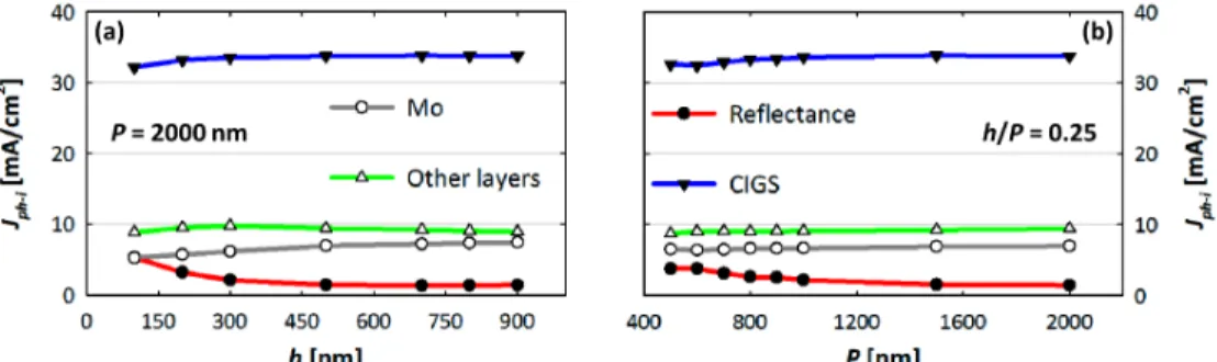
The analysis continued with the optimization of the grating dimensions. With P set at 2000 nm, a series of models differing only in h were run. Results are summarized in Fig. 5(a), where the implied photocurrent density generated or lost in each cell layer (Jph–i), calculated
using Eq. (2), is plotted as function of h:
• Reflectance losses decrease for larger values of h, because taller gratings have better light in-coupling properties. However, having height values larger than 500 nm does not appear to have additional benefits in this respect.
• Losses in the Mo back contact increase with h, because taller structures can couple more light onto the surface of the metal.
• Losses in other layers remain approximately constant and no clear dependency on h can be observed.
The best performance (Jph-CIGS = 33.9 mA/cm2) is achieved for h = 500 nm. For larger
values of h, Jph-CIGS remains almost unchanged.
A similar analysis to evaluate the effect of the grating period (P between 500 nm and 2000 nm) was conducted. In this case, the grating height-to-period ratio was kept constant at 0.25, so that all gratings have the same aspect ratio. Results are depicted in Fig. 5(b):
• Losses in Mo an other non-active layers remain constant for all P values. This suggests that light coupling on Mo surface layer does not depend on the grating height, but rather on h/P (i.e. the aspect ratio of the periodic features).
• Reflectance reduces for larger values of P, for which the refractive index grading is smoother and, consequently, more light can be coupled into the device.
In conclusion, the best results were achieved for the 1-D grating with P = 2000 nm and h = 500 nm. It must be noted that a similarly high performance was achieved for a smaller grating period of 1500 nm. However, it was decided to prefer the larger value of 2000 nm, which will allow for the growth of a higher quality material in manufactured devices as mentioned above.
Fig. 5. Summary of geometrical optimization of gratings height (a) and period (b).
The study was extended to 2-D gratings. Pyramidal periodic features were employed, with the same dimensions of the previously optimized 1-D gratings: period of 2000 nm and height of 500 nm. A sketch of the structure can be observed in Fig. 6 on the left. In particular, tiny regular (i.e. not pseudorandom) truncated pyramids modelling the self-roughness of front CIGS surface are visible. These were also deployed in the simulated models based on 1-D gratings. An initial study, not reported here for brevity, showed no difference in simulated
spectra when using pseudorandom or regular truncated pyramids in models based on periodic gratings. For ease of implementation in our 3-D models, a regular arrangement was chosen.
While 2-D gratings could be more complicated to manufacture, they offer some advantages over 1-D structures. In particular, they can diffract more light away from the incident direction and also excite a higher number of guided modes in the absorber. Results of this work, depicted in Fig. 6, show that the pyramidal 2-D grating can further suppress reflectance when compared to 1-D structures. In this way almost all incident light is coupled into the device. However, since reflectance was already very low in the case of triangular 1-D gratings, the benefits in term of Jph-CIGS are relatively small (1-D best case: 33.9 mA/cm2, 2-D
case: 34.2 mA/cm2). Nevertheless, a careful observation of A
CIGS of both textured solar cell
models shows the presence of a small peak in the 1100-1150 nm region of the spectrum. This peak is more pronounced for the model endowed with 2-D grating, suggesting that light diffraction and wave-guiding phenomena are taking place more strongly than in 1-D grating case. To further investigate this, light propagation inside the models was analyzed.
Fig. 6. 3-D rendering of the pyramidal (2-D) grating model (left) and comparison between simulated CIGS absorptance and cell reflectance of the 1-D and 2-D grating solar cells.
3.3. Eigenmode analysis
Solar cells can support a large variety of optical modes, which display different electromagnetic field distributions [33]. The capacity to produce guided-mode resonances in the absorber layer is a key advantage of periodic gratings over random texturing, and usually explains the absorption enhancement which results from their application.
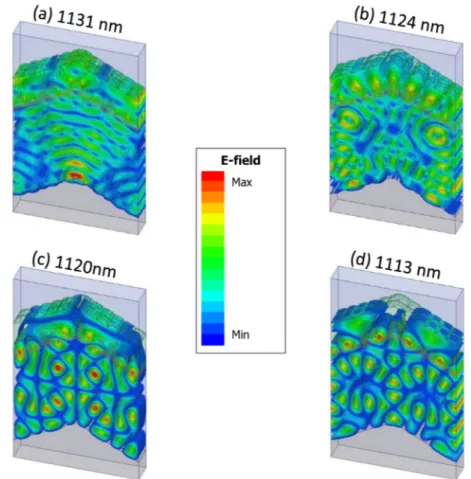
In this work, eigenmode simulations were carried out to provide an insight into the resonances which can arise in the modelled devices due to the presence of gratings. The ‘Eigenmode Analysis’ mode in HFSS does not seek all computable eigenmodes of a structure. Rather, both the number of eigenmodes and the minimum frequency are user-defined, thus limiting the analysis to a certain (narrow) frequency (wavelength) range of interest. To make the analysis clear and visual, the study was limited to model with 1-D triangular gratings. Only the spectral range around the peak observed in Fig. 6 (~1130 nm) was considered.
Results of the eigenmode analysis showed an extremely dense population of resonant modes, as can be seen in Fig. 7. For a selected number of these modes the electric field distribution, which is here used to represent light propagation in the device, was looked into:
• At λ = 1131 nm, it is possible to observe diffraction by the symmetric facets of the grating, which affects the propagation direction of the plane waves inside the CIGS absorber.
• At λ = 1124 nm, a wave-guide pattern that extends from the absorber into the ZnO:Al can be noticed. While wave-guiding in the CIGS absorber leads to an increase in J ph-CIGS, guided modes excited into the front TCO are undesired, leading to parasitic
absorption losses.
• At λ = 1120 nm and λ = 1113 nm, hybridized diffraction and wave-guided resonances appear, similar to what observed by Brongersma et al. in their simulation work [33]. The distribution at λ = 1113 nm is of particular interest, displaying a five-fold symmetric field pattern near the apex of the grating. The presence of this optical resonance can lead to significant absorption enhancement in the CIGS layer.
Fig. 7. Electric field magnitude for selected wavelengths: (a) eigenmode @ 1131 nm, exhibiting a diffraction pattern from gratings’ facets; (b) eigenmode @ 1124 nm, showing wave-guiding in both absorber and front TCO; (c) eigenmode @ 1120 nm and (d) eigenmode @ 1113 nm, where hybridized diffraction and wave-guided resonances can be observed.
The ‘Eigenmode analysis’ carried out showed that the presence of 1-D periodic structures can excite several resonant modes inside the solar cell. Each of this modes exhibits different field patterns and can lead to a significant enhancement of the device absorptance. It is safe to assume that, in the presence of 2-D gratings, even more resonances can be excited. This will result in further increasing of the solar cell performance, as observed in Fig. 6.
3.4. Alternative cell configurations
Despite improvements in anti-reflection achieved by means of periodic gratings, further increase of the absorptance in the CIGS layer is prevented by high parasitic absorption in supporting layers, particularly in the Mo back reflector and in the ZnO:Al front TCO, as can
be observed in Fig. 4. For this reason, alternative cell configurations which mitigate or eliminate these losses are of great interest. The use of (i) a dielectric spacer layer between absorber and metal, (ii) Mo-free back reflectors, and (iii) highly transparent front TCOs are investigated in this section.
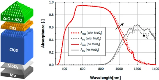
Fig. 8. Sketch of the model with 2-D pyramidal gratings and MoO3 spacer layer (left) and simulation results (right). The introduction of the dielectric spacer layer reduced the parasitic absorptance inside Mo (grey lines) and increased absorption in the CIGS layer (red lines).
Molybdenum is the conventional metallic back reflector / back contact used in CIGS solar cells: it allows for the growth of large CIGS grains, it remains inert during deposition [34], and forms an ohmic contact for the majority charge carriers (holes) through the formation of an intermediate MoSe2 layer [35,36]. On the other hand, it exhibits lower reflectance with
respect to other metals (e.g. Ag). This results in relatively high parasitic absorption losses [34], as also shown in the simulations presented in the previous section of this manuscript. Replacement of Mo with alternative materials remains a challenge, but several possibilities have been investigated. Metals like W, Ta and Nb are promising, since they remain inert during CIGS deposition. However, they do not appear to offer clear advantages with respect to Mo [34]. Other metals are less stable at the high temperatures and Se-rich atmospheres typical of CIGS deposition, and their diffusion into the absorber layer would cause a significant degradation of the cell performance.
Absorption in metallic (textured) back reflectors may be reduced using a dielectric spacer layer between the absorber and the metallic reflector, as commonly done in wafer-based and thin-film silicon solar cells [37–39]. Requisites of this spacer are high vertical conductivity and transparency. Investigations of ZnO/Mo back contacts have been conducted, as well as ZnO/Ag [9]. In this work, the potential of molybdenum trioxide (MoO3) as spacer layer
between CIGS and Mo was tested. MoO3 is a transparent material with relatively high
temperature stability and low absorption, particularly at long wavelengths as can be seen in Fig. 2; it also has sufficiently high vertical conductivity [40], making it suitable as back transparent conductive oxide.
A 80-nm thick MoO3 buffer layer is tested in a 2-D grating cell model, presented in Fig. 8;
grating dimensions are P = 2000 nm and h = 500 nm. Two models, one with spacer layer and one without, were compared. A preliminary study determined that 80 nm was the optimal thickness, guaranteeing sufficient hole conductivity and quenching of molybdenum absorptance (AMo). Simulation results of the abovementioned 2-D gratings based models,
shown in Fig. 8, indicate that the presence of the MoO3 layer effectively reduces AMo. As a
generated inside the CIGS layer increases from 34.2 mA/cm2 (no spacer layer) to 34.8
mA/cm2 (80-nm thick MoO
3 spacer layer).
Table 2. Cell layer thicknesses for configurations B, C, and D.
Layer Material Thickness [nm] Back reflector Ag 300
Substrate Glass 300 Back TCO ITO/IOH 80
Absorber CIGS 1500
Buffer layer CdS 50
Window ZnO 50
Front TCO ZnO:Al/IOH 450/80
A complete removal of Mo from the back reflector could further improve the device optical performance. To this purpose, configurations using a TCO deposited directly on the substrate were investigated. To prevent transmittance losses at the back side, a thin layer (~300 nm) on silver is added on the opposite side of the glass carrier. In this way diffusion of the metal into the cell layers can be prevented [5,9]. At the same time, the high reflectivity of the Ag layer guarantees that no light is transmitted at the back side of the device. Two different TCO materials were tested: tin-doped indium oxide (In2O3:Sn, ITO) and
hydrogenated indium oxide (In2O3:H, IOH). Both materials have high conductivity and
transparency [41,42], but IOH has lower free-carrier absorption in the near infrared region of the spectrum. On the other hand, ITO has higher stability at elevated temperatures and has already been successfully tested as back contact for in thin-film CIGS solar cells [43].
Fig. 9. Different simulated cell configurations (not to scale). These sketches should be imagined as cross-section of the models based on 2-D gratings.
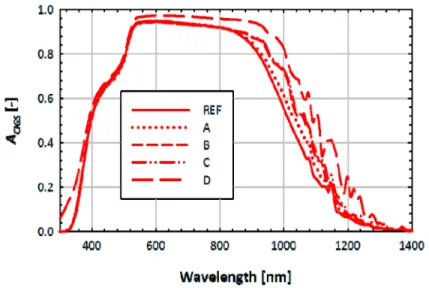
Various alternative configurations were analyzed and compared. ‘REF’ indicates the reference device on optimized 2-D gratings with a Mo back reflector as shown in Fig. 6, while ‘A’ refers to the optimized device with the 80-nm thick MoO3 buffer layer as shown in Fig. 8.
‘B’ is a model with the same pyramidal periodic structures, but employs ITO as back contact and a silver layer behind the glass substrate to ensure high reflectivity at the back side. Model ‘C’ is identical to ‘B’, but the ITO layer has been here replaced by an IOH back TCO. These configurations are depicted in Fig. 9, while layer thicknesses are summarized in Table 2.
Building a realistic model with the glass/Ag back reflector configuration in 3-D Maxwell equations solvers would result in an unwieldy large structure which would strain computational resources – this is due to the necessarily large thickness of the glass layer (millimeter scale, as opposed to the nanometer scale of other layers). To avoid extraordinarily long meshing and solving times, the simulated cells have 300-nm thick glass. Thanks to the presence of 2-D gratings on this necessarily thin substrate, interference phenomena are suppressed, thus ideally modelling an incoherent propagation of light as in an equivalent bulk
glass substrate. In addition, the silver layer is treated as a perfectly conductive layer. As a result, the absorption of the ideal Ag reflector and transmission at the back reflector are exactly zero. While these are necessary approximations, results can be considered reliable since Ag has a very high reflectivity, particularly in the near infrared part of the spectrum and millimeter-thick glass carrier would only absorb a very small amount of light.
Fig. 10. ACIGS of devices with different configurations. Modifications to the back reflector improve performance at long wavelengths (‘A’, ‘B’, ‘C’), while using IOH as front TCO (‘D’) results in an increase of ACIGS over the whole spectrum.
Results of the simulations, presented in Fig. 10, showed that the Mo-free back reflector configurations (‘B’ and ‘C’) perform better than structure where Mo is included (‘REF’ and ‘A’). At short wavelengths all models have similar ACIGS. However, the advantage of the
Mo-free architectures becomes evident in the long-wavelength region (λ > 850 nm), where molybdenum would be parasitically absorbing. Absorptance in CIGS for the Mo-free models is increased in this spectral region, which translates into an increase of Jph-CIGS: from 34.8
mA/cm2 (model ‘A’) to 35.6 mA/cm2 (model ‘B’) and 35.7 mA/cm2 (model ‘C’). The
performance of the devices with ITO and IOH back TCOs are very similar, with the latter showing only a slight improved performance due to the higher infrared transparency of IOH.
In addition to the Mo absorption, losses in the AZO front TCO and the CdS buffer layer contribute to reducing the photocurrent density generated in the CIGS layer. For the TCO, the ZnO:Al layer needs to be relatively thick (> 200 nm) to guarantee sufficient electron conductivity and good electrical performance. The IOH TCO, owing to its high carrier mobility, can be made 80-nm thick [44] to provide with sufficient sheet resistance for lab-scale devices such as the ones investigated in this contribution. Combined with its high transparency (i.e. low extinction coefficient κ, see Fig. 2), the IOH is an ideal candidate as front TCO in thin-film solar cells. In the work here presented, the 400 nm thick ZnO:Al layer was substituted with an 80-nm thick IOH front TCO, while at the back side the IOH/glass/Ag configuration was employed, which corresponds to model ‘D’ in Fig. 9. Simulations showed that this yields an increase of the absorption in the CIGS layer over the whole spectral range, as depicted in Fig. 10, since the highly-transparent front layer allows more light to enter the absorber. Integration with AM1.5 photon flux results in an Jph-CIGS for configuration ‘D’ of
38.6 mA/cm2. This value represents an increase of 7.9 mA/cm2 ( + 26%) over the
non-textured calibrated device. Recent studies have shown that it is possible to substitute the CdS buffer layer with more transparent materials, without sacrificing the device electrical performance [45,46]. These architectures, however, are not investigated in this work to allow a direct comparison of models and reference (manufactured) device.
3.5 Reduction of CIGS thickness
Scarcity of indium could prevent the widespread diffusion of Cu(In,Ga)Se2 technology in the
PV market. Reduction of the absorber thickness while maintaining high absorption levels can help decreasing production costs and promoting diffusion of CIGS solar cells.
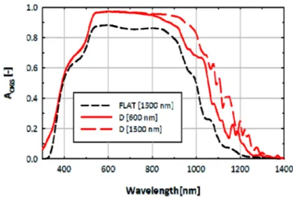
To verify the effectiveness of the approach presented in this work to this purpose, the performance devices with sub-micron thick absorbers was investigated. Thicknesses of CIGS down to 600 nm were tested, in a cell configuration with IOH used as both front and back TCO (model ‘D’ in Fig. 9). As can be observed in Fig. 11, the thinner architecture (600 nm) maintained the high performance of the thicker device (1500 nm) up to λ = ~800 nm. For longer wavelengths a decrease of ACIGS can be noticed, as expected since this is the region of
the spectrum where CIGS absorptance becomes weaker. Nevertheless, the solar cell model with a 600-nm thick absorber still outperformed a much thicker flat non-optimized (AZO front TCO and Mo back reflector) device (included in Fig. 11 as a black dotted line, for reference). The implied photocurrent densities calculated are 36.4 mA/cm2 (thin device) and
30.7 mA/cm2 (flat thick reference) .
Fig. 11. Absorptance in CIGS for cells with configuration ‘D’ and absorber thickness of 600 nm and 1500 nm. ACIGS of the flat calibration model is included as reference.
This shows how, by careful optimization of periodic gratings and materials in the supporting layers, it is possible to obtain substantial improvement of the optical performance (ΔJph-CIGS = + 5.7 mA/cm2) and, at the same time, reduce the utilization of material in the
device (–60% CIGS thickness). At this point it should be noted, however, that effective implementation of IOH inside the architecture of Cu(In,Ga)Se2 thin-film solar cells requires
careful investigation. The study here presented showed the benefits of including this material in the device configuration, resulting in the reduction of parasitic absorption in the front TCO and in the elimination of Mo from the back reflector. However, only experimental analysis of devices with IOH front and back TCO will be able to determine if the solutions proposed in this work can be applied in real devices.
4. Conclusions
A satisfactory optical model of a real thin-film CIGS solar cell in HFSS environment was presented. Relatively good match between the simulated absorptance and reflectance and measurements was obtained. These results were only achieved with a pseudorandom texture model, necessary to include the effect of random self-roughness of CIGS and other layers on the propagation of light.
The results of the application of gratings to the solar cell models led to the following conclusions: (i) the application of 1-D and 2-D periodic gratings results in anti-reflective effect and enhanced CIGS absorption. 2-D structures showed a little performance improvement over their 1-D counterparts; (ii) the implied photocurrent density in the absorber increases with the height and period of the grating in general. These trends appear to level out for values of the period greater than the absorber thickness (1500 nm) and of the grating height-to-period ratio over 0.25; (iii) for all models, improvements in CIGS absorption and device anti-reflection are accompanied by increased absorption in the molybdenum layer.
The eigenmode analysis confirmed the excitation of a dense population of resonances in the cell structure due to the usage 1-D (2-D) periodic texture. The electric field distributions of the periodic texture simulation also showed a diverse range of configurations, highlighting the different light propagation phenomena induced by the presence of the gratings.
Table 3. Implied CIGS absorber photocurrent density for selected models.
Cell CIGS thickness [nm] Jph-CIGS[mA/cm2] Gain [%]
Calibration 1500 30.7 -
1-D 1500 33.8 9.4
2-D [‘REF’] 1500 34.2 11.0
2-D + MoO3 [‘A’] 1500 34.8 13.0 2-D IOH back [‘C’] 1500 35.7 15.9 2-D IOH front & back [‘D’] 1500 38.6 25.3 2-D IOH front & back [‘D’] 600 36.4 18.2
The poor performance of Mo as back reflector remains an obstacle to efficiency improvements in typical CIGS device. However, the use of MoO3 as a dielectric spacer
between absorber and back reflector has been shown in simulations to reduce parasitic losses in the Mo back contact. Nevertheless, absorption in Mo remains high and its replacement with alternative configurations (TCO/glass/metal) can further increase the device performance. The front ZnO:Al TCO is also a major source of parasitic absorption losses in standard CIGS solar cells. Significant improvements can be achieved when a more transparent and conductive material like IOH is employed. Benefits are evident in a wide spectral range, since more light is allowed to enter the absorber and contribute to the photocurrent density generation.
Lastly, simulations of cells with reduced CIGS absorber thickness of 600 nm indicate that the cumulative impact of the modelled light management techniques can result in devices which exceed the photocurrent density of the 1500-nm thick reference flat absorber. These results, as illustrated in Table 3, indicate that the optical performance, and subsequently photocurrent density and efficiency of state-of-the-art CIGS solar cells can be further improved by the application of optimized periodic textures and the use of improved materials in the cell stack. Integration of this materials in the cell architecture, however, as well as the additional parasitic losses resulting from encapsulation of the device, need to be further investigated by modelling and experimental analysis.
Acknowledgments
The research leading to these results has received funding from the European Union's Seventh Framework Program FP7/2007-2013 under grant agreement n° 261901 (AGATHA). The authors thank prof. H. Fujiwara (Gifu University) for useful discussions.