HAL Id: cea-02340816
https://hal-cea.archives-ouvertes.fr/cea-02340816
Submitted on 31 Oct 2019HAL is a multi-disciplinary open access archive for the deposit and dissemination of sci-entific research documents, whether they are pub-lished or not. The documents may come from teaching and research institutions in France or abroad, or from public or private research centers.
L’archive ouverte pluridisciplinaire HAL, est destinée au dépôt et à la diffusion de documents scientifiques de niveau recherche, publiés ou non, émanant des établissements d’enseignement et de recherche français ou étrangers, des laboratoires publics ou privés.
Low-temperature deposition of transparent conductive
layers for perovskite-silicon tandem cells
Jonas van Stappen, Chloé Dindault, Tiphaine Bourgeteau, Heejae Lee, Denis
Tondelier, Bernard Geffroy, Yvan Bonnassieux
To cite this version:
Jonas van Stappen, Chloé Dindault, Tiphaine Bourgeteau, Heejae Lee, Denis Tondelier, et al.. Low-temperature deposition of transparent conductive layers for perovskite-silicon tandem cells. SPIC 2017 (Science et Technologie des Systèmes pi-Conjugués), Oct 2017, Limoges, France. �cea-02340816�
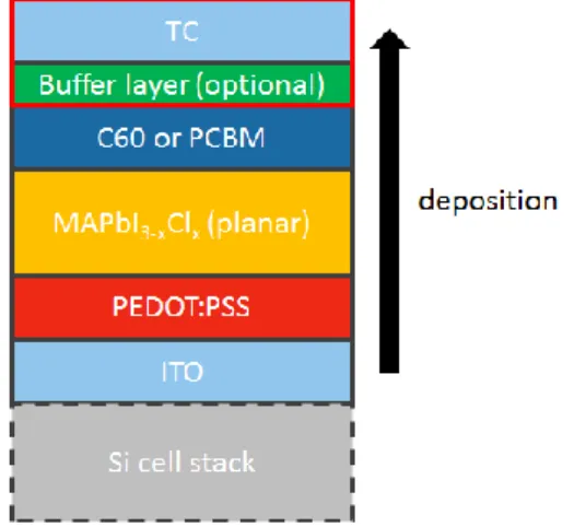
Figure 1 – MAPbI3-xClx cell stack used in this work, with the focus of this contribution
highlighted by the red frame.
Low-temperature deposition of transparent conductive
layers for perovskite-silicon tandem cells
Jonas van Stappen,
1,* Chloé Dindault,
1,2Tiphaine Bourgeteau,
1Heejae Lee,
1Denis
Tondelier,
1,* Bernard Geffroy,
1,3Yvan Bonnassieux
11
LPICM, CNRS, Ecole Polytechnique, Université Paris-Saclay, 91128 Palaiseau Cedex, France 2
Institut Photovoltaïque d’Ile de France (IPVF), 92160 Antony, France 3
LICSEN, NIMBE, CEA, CNRS, Université Paris-Saclay, CEA Saclay, 91191 Gif-sur-Yvette Cedex, France
* Corresponding authors, mail: [email protected] and [email protected]
Since 2013, single-junction research-cell power conversion efficiencies of perovskite cells have risen by about 8%abs to 22.1%, while multicrystalline silicon and monocrystalline silicon efficiencies have risen by less than 2%abs and less than 1%abs, respectively [1]. Tandem cells with a perovskite top cell and a silicon bottom cell, recently achieving 23.6% in two-terminal configuration, present a promising alternative to further increase the relatively stagnant performance of already highly-optimized single-junction silicon cells [2]. To facilitate
such an advance, methods to deposit high-quality transparent conductors (TCs) which do not subject the perovskite layer to degradation during deposition need to be found.
We utilize a spin-coating solution deposition process optimized for high reproducibility, yielding the single-junction MAPbI3-xClx perovskite cell stack shown in Figure 1, with an average efficiency of 7.94 ± 0.68 % with a non-transparent electrode. Two different TC electrodes are tested on these cells: evaporated thin-film semi-transparent Ag layers and low-temperature RF-sputtered indium tin oxide layers. For the latter, buffer layers of either thin-film Ag, Ag/BCP, Ag nanowires or interlinked PCBM are used to protect the organic layer stack from sputtering damage.
By comparing transparency and efficiency, we will identify the most suitable approach. References
[1] M. A. Green, K. Emery, Y. Hishikawa, W. Warta, E. D. Dunlop, D. H. Levi and A. W. Y. Ho-Baillie, Solar cell efficiency tables (version 49). Prog. Photovolt: Res. Appl. (2017), 25: 3–13. doi: 10.1002/pip.2855
[2] K. A. Bush, A. F. Palmstrom, Z. J. Yu, M. Boccard, R. Cheacharoen, J. P. Mailoa, D. P. McMeekin, R. L. Z. Hoye, C. D. Bailie, T. Leijtens, I. M. Peters, M. C. Minichetti, N. Rolston, R. Prasanna, S. Sofia, D. Harwood, W. Ma, F. Moghadam, H. J. Snaith, T. Buonassisi, Z. C. Holman, S. F. Bent, M. D. McGehee,