HAL Id: hal-02953160
https://hal.archives-ouvertes.fr/hal-02953160
Submitted on 30 Sep 2020HAL is a multi-disciplinary open access archive for the deposit and dissemination of sci-entific research documents, whether they are pub-lished or not. The documents may come from teaching and research institutions in France or
L’archive ouverte pluridisciplinaire HAL, est destinée au dépôt et à la diffusion de documents scientifiques de niveau recherche, publiés ou non, émanant des établissements d’enseignement et de recherche français ou étrangers, des laboratoires
LFoundry 150 nm and TowerJazz 180 nm CMOS
Technologies
T. Wang, M. Barbero, P. Barrillon, I. Berdalovic, C. Bespin, S. Bhat, P.
Breugnon, I. Caicedo, R. Cardella, Z. Chen, et al.
To cite this version:
T. Wang, M. Barbero, P. Barrillon, I. Berdalovic, C. Bespin, et al.. Depleted Monolithic Active Pixel Sensors in the LFoundry 150 nm and TowerJazz 180 nm CMOS Technologies. 28th International Workshop on Vertex Detectors, Oct 2019, Lopud Island, Croatia. pp.026, �10.22323/1.373.0026�. �hal-02953160�
PoS(Vertex2019)026
Depleted Monolithic Active Pixel Sensors in the
LFoundry 150 nm and TowerJazz 180 nm CMOS
Technologies
T. Wang∗a, M. Barberob, P. Barrillonb, I. Berdalovicc, C. Bespina, S. Bhatb,
P. Breugnonb, I. Caicedoa, R. Cardellac, Z. Chenb, Y. Degerlid, J. Dingfeldera,
L. Flores Sanz de Acedoc, S. Godiotb, F. Guillouxd, T. Hempereka, T. Hironoa,
F. Hügginga, H. Krügera, T. Kugathasanc, K. Moustakasa, A. Ouraoud, P. Pangaudb,
H. Perneggerc, F. Piroc, D-L. Pohla, P. Riedlerc, P. Rymaszewskia, P. Schwemlingd, W. Snoeysc, M. Vandenbroucked, N. Wermesaand S. Zhanga
aPhysikalisches Institut, University of Bonn
Nußallee 12, 53115 Bonn, Germany
bAix Marseille University, CNRS/IN2P3, Centre de Physique des Particules de Marseille
163 Avenue de Luminy, Marseille, France
cCERN
CH-121 Geneve 23, Switzerland
dIRFU, CEA-Saclay
Gif-sur-Yvette Cedex, 91191 France
E-mail:t.wang@physik.uni-bonn.de
The monolithic CMOS pixel sensor for charged particle tracking has already become a mainstream technology in high energy particle physics (HEP) experiments. During the last decade, progressive improvements have been made for CMOS pixels to deal with the high-radiation and high-rate environments expected, for example, at the future High Luminosity LHC. One of the key ingredients of these improvements is to achieve a fully depleted sensitive layer, where the charge collection is guided by strong drift field lines. CMOS sensors incorporating such charge collection property, often referred to as DMAPS (Depleted Monolithic Active Pixel Sensor), have been recently demonstrated in several large-scale monolithic prototypes with integrated fast readout architectures. This contribution summarizes the recent progress made on the large-scale DMPAS development, focusing on two demonstrator chips designed in the LFoundry 150 nm and the TowerJazz 150 nm CMOS processes, namely LF-Monopix1 and TJ-Monopix1.
The 28th International Workshop on Vertex Detectors - Vertex2019 13-18 October, 2019
Lopud, Croatia
∗Speaker.
c
Copyright owned by the author(s) under the terms of the Creative Commons
PoS(Vertex2019)026
1. Introduction
CMOS pixel sensors utilizing commercial CMOS processes have been realized in the late 1990s for high precision charged particle tracking in HEP experiments [1]. By taking advantage of fabricating sensor elements and complex electronic devices on the same silicon substrate, they have naturally evolved towards forming a detection system on a single chip, i.e. a fully monolithic detector, which allows for low material budget, low cost and easy module assembly as compared to the hybrid pixel technology. However, the existing mature devices, like the MIMOSA28 chip used in the STAR experiment at the RHIC collider [2] and the ALPIDE chip being installed for the ALICE experiment at LHC [3], cannot withstand the high particle rate and high radiation environment encountered, for example, at the future High Luminosity LHC (HL-LHC). The main limiting factor for these devices is the predominant diffusion movement for charge collection. Hence, during the last decade, there has been a trend to improve the depletion within the sensitive layer of CMOS pixels [4], leading eventually to designs with fast charge collection through drift, namely DMAPS. Recently, significant progress has been made for DMAPS devices with several large-scale demonstrator chips developed in different CMOS technologies [5–9]. These devices combine a fully depleted sensitive layer with on-chip fast readout electronics, and are expected to tolerate particle fluences of at least 1015neq/cm2 and total ionization doses of at least 80 Mrad,
while being able to cope with a particle rate higher than 100 MHz/cm2 and distinguish hits from different LHC bunch crossings (25 ns). This contribution summarizes the DMAPS development made in the LFoundry 150 nm CMOS technology and the TowerJazz 180 nm CMOS technology, exemplified by two demonstrator chips called LF-Monopix1 and TJ-Monopix1.
2. Sensor design approaches
The depth of the depleted sensing volume can be approximately described by d ∝√ρ V , where d is the depletion depth, ρ is the resistivity of substrate and V the bias voltage. Thus, it is natural for CMOS pixels to utilize the high resistivity and high voltage features steadily offered by the commercial CMOS processes [10, 11]. In this section, the two design approaches we have been following to achieve a fully depleted sensing layer are described. The design of large-scale fully monolithic prototypes employing these two approaches are also described.
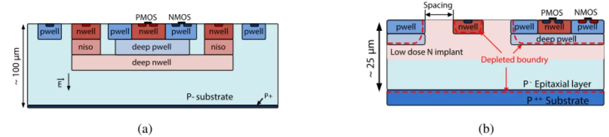
2.1 The large electrode approach in the LFoundry 150 nm CMOS technology
The development of DMAPS in LFoundry 150 nm CMOS technology makes use of a so-called large electrode design to achieve a depleted sensitive layer by combining high resistivity substrate (> 2 kΩ cm) as the sensitive layer and high bias voltage (> 200 V). As shown in figure1(a), the implemented sensor structure mimics the standard planar sensor, and it incorporates a large-area n-type implant (deep nwell) as the collection node, which is an intrinsically radiation-hard structure with uniform drift field within the sensitive volume. The in-pixel electronics is integrated in the collection well thanks to the multiple nested wells offered by the foundry. In particular, the available deep pwell shields the nwells for PMOS transistors from the deep nwell, and allows for full CMOS circuit inside the pixel.
PoS(Vertex2019)026
DMAPS in the LFoundry 150 nm and TowerJazz 180 nm CMOS Technologies T. Wang
nwell
pwell nwell nwell pwell
niso niso deep nwell deep pwell pwell pwell P- substrate E P+ ~ 1 00 μ m NMOS PMOS (a) nwell deep pwell pwell nwell pwell
NMOS pwell
PMOS Spacing
Low dose N implant
P-Epitaxial layer P++Substrate Depleted boundry ~ 2 5 μm (b)
Figure 1: Cross-sectional view of the pixel design using(a)the large electrode approach in the LFoundry
150 nm CMOS technology and(b)the small electrode approach in a modified 180 nm CMOS process from
TowerJazz. The blue region indicates p-type material and the red region indicates n-type material. The
process modification in(b)includes a low dose n-type implant in addition to the standard process.
2.2 The small electrode approach in the TowerJazz 180 nm CMOS technology
The TowerJazz DMAPS development line is derived from the ALPIDE development [3]. As shown in figure1(b), it uses a small nwell as the charge collection node, and the resulting sensor capacitance is ∼ 5 fF or smaller, a value typically more than an order of magnitude smaller than that in a large electrode design. A major benefit of small sensor capacitance is the possibility to employ an ultra-low power analog front-end design (∼ 1 µW/pixel to adequately distinguish hits from different 25 ns time intervals), maintaining at the same time good noise, threshold and timing performance. The sensing layer in this case is a high-resistivity (> 1 kΩ cm) p-type epitaxial layer with typical thickness of 25 - 30 µm. The in-pixel electronics is implemented outside the collection electrode, and the availability of deep pwell as a shielding layer allows for full CMOS circuit inside the pixel. In order to enhance the depletion level, moderate reverse bias (e.g. 6 V) can be applied at the p-type substrate and the pwells. However, a fully depleted sensitive layer requires dedicated process modifications. Figure1(b) shows a modification scheme which adds a low dose n-type implant. Details of such process modifications are described in [12].
3. Design of large-scale demonstrator chips
We have followed both of the aforementioned sensor design approaches and developed two large-scale demonstrator chips named LF-Monopix1 and TJ-Monopix1, respectively. Both chips integrate a fast readout architecture called “column drain” readout, which is similar to the one established for the ATLAS pixel readout chip FE-I3 [13].
Figure2depicts the chip architecture and the pixel schematic diagram shared by the LF- and TJ-Monopix1 chips. The pixel contains both the sensing element and the readout electronics. The charge signal collected from the sensing node is converted into a voltage pulse by a preamplifier, which is then sent to a discriminator circuit that fires when the pulse height exceeds a preset threshold value. An edge detector following the discriminator generates two short pulses, LE and TE, corresponding to the leading edge and trailing edge of the discriminator output respectively. These two pulses strobe the value on the BCID bus into the in-pixel RAM cells, stamping the time of arrival (ToA) and time over threshold (ToT) of the hit. The BCID bus represents the bunch crossing identifier, which carries the signal outputs from a gray counter running at 40 MHz. The hit
PoS(Vertex2019)026
pixels in the column are read out one by one, arbitrated by a token passing scheme. More details of the chip design are described in [5, 6].
Figure 2: The chip architecture and schematic diagram of the two Monopix1 prototypes. The lower right corner shows the timing for operation.
Table3 lists the main parameters of the two Monopix1 chips. As mentioned in section2.2, using the small electrode approach allows for low power analog front-end circuit. In case of TJ-Monopix1, the static current consumption per pixel is less than 1 µA, whereas the pixel static current for LF-Monopix1 is about 20 µA in order to have a fast peaking time ∼ 25 ns with the large sensor capacitance estimated to be ∼ 400 fF. In addition, the small electrode design allows for small pixel size, thanks to the small footprint of the sensing element and a very compact analog front-end circuit derived from the ALPIDE chip [3]. But it should be noted that the pixel size for LF-Monopix1 was chosen to be the same as that of the ATLAS FE-I4 chip [14], and a smaller pixel size is still possible.
LF-Monopix1 TJ-Monopix1
Sensor type large electrode small electrode
Chip size ∼ 1 cm × 1 cm ∼ 1 cm × 2 cm
Pixel size 50 µm × 250 µm 36 µm × 40 µm
Matrix size 129 rows × 36 columns 224 rows × 448 columns
Est. sensor capacitance ∼ 400 fF < 5 fF
Analog current ∼ 20 µA/pixel < 1 µA/pixel
PoS(Vertex2019)026
DMAPS in the LFoundry 150 nm and TowerJazz 180 nm CMOS Technologies T. Wang
4. Measurement results
Both LF-Monopix1 and TJ-Monopix1 chips have been extensively measured before and after irradiation. This section summaries some important results obtained. Lessons learned will also be discussed.
4.1 Results for LF-Monopix1 4.1.1 I-V curves
A high bias voltage is essential to ensure a large depleted sensing volume and a high charge collection field. Dedicated studies concerning the optimization of the guard ring design have been performed in order to improve the breakdown behavior of the sensor [15]. Figure3(a) shows the I-V curve measurements obtained from three chip samples, two of which are taken from back-side processed wafers having thicknesses of 200 µm and 100 µm, respectively. In all three cases, the breakdown voltage is higher than 250 V and the differences between these chips are within the range of fluctuation due to wafer-to-wafer and chip-to-chip variations. For irradiated chips, as shown in figure3(b), the I-V curves are only measured up to 200 V, in order to limit the current consumption and protect the chips from thermal runaway. It is noted that breakdown voltage is expected to be higher for irradiated chips, and a bias voltage beyond 400 V has already been easily applied on dedicated test sensors for bare sensor performance studies [16, 17].
(a) (b)
Figure 3: (a)I-V curves measured for chip samples with different thickness before irradiation. (b) I-V
curves for a neutron irradiated chip, a proton irradiated chip and an unirradiated chip for comparison. The
measurements for(b)have been performed in a climate chamber at an atmospheric temperature of -25◦C.
4.1.2 Efficiency
The hit detection efficiency was measured with a 2.5 GeV electron beams at the Bonn Electron Stretcher Accelerator ELSA facility. Figure4 shows the efficiency map measured for both an unirradiated chip and a chip irradiated with neutrons up to a fluence of 1015neq/cm2. The threshold
was tuned to 1800 e−and 1600 e−for the unirradiated and the neutron irradiated chip, respectively. At these thresholds, the noise occupancy levels of the chips are much lower than 40 Hz/pixel, a
PoS(Vertex2019)026
value typically required for the p-p experiments at HL-LHC. The chips were cooled down to lower than -40◦C by dry ice. During the threshold tuning, pixels with very high noise were disabled (masked). This has resulted in a few low efficiency rectangular shapes in figure4 due to masked pixels and these regions are excluded from the efficiency calculation. The percentage of masked pixels is kept below 1%. The average hit detection efficiencies are (99.7±0.1)% and (98.9±0.1)% for the unirradiated and the irradiated chip, respectively. The dominant error of this measurement is due to misassignment between the beam track extrapolation and a given hit in LF-Monopix1.
(a) (b)
Figure 4: Hit detection efficiency map of(a)an unirradiated and(b) a neutron irradiated (1015n
eq/cm2)
LF-Monopix1 chip. Detection efficiencies are (99.7±0.1)% and (98.9±0.1)% for the unirradiated and irradiated chip, respectively. Inefficient regions correspond to masked pixels. Five and one pixel were masked in the unirradiated and irradiated chip, respectively. The masked regions and edges of measured area were excluded from the efficiency calculation.
Figure5shows the in-pixel efficiency close to the region of the joint corner among 2 × 2 pixels. In order to increase the statistics, data of multiple 2 × 2 pixels are superimposed. Before irradiation, high efficiency has been achieved uniformly throughout the pixels. After irradiation, as shown in figure5(b), only a slight efficiency drop can be observed, which is more visible at the pixel corner due to charge trapping and charge sharing among multiple pixels, rendering less signal charge to be collected by a single pixel.
4.2 Results for TJ-Monopix1
4.2.1 Noise and threshold measurement
The noise performance and threshold distribution has been studied by injecting an external voltage pulse on a test injection capacitor in each pixel. The probability of pixel firing can be recorded as a function of the injection amplitude, forming the so-called "S curves". The noise and threshold parameters of each pixel can be extracted by fitting the corresponding "S curve" with the error function, after calibrating the injection circuit with an55Fe radioactive source.
Figure6 shows the noise and threshold distribution for a sub-matrix with the deep pwell partially removed under the pwells close the sensing node. Before irradiation, the average noise
PoS(Vertex2019)026
DMAPS in the LFoundry 150 nm and TowerJazz 180 nm CMOS Technologies T. Wang
(a) (b)
Figure 5: In-pixel efficiency close to the joint corner of 2 × 2 pixels for (a) an unirradiated chip and
(b) a neutron irradiated (1015neq/cm2) chip. The hit efficiency for the unirradiated chip is homogeneous
throughout the pixels. For the irradiated chip, there is only a slight efficiency drop at the pixel corner.
is 16 e−, which agrees well with the simulated value. After a particle fluence of 1015neq/cm2, as
shown in figure6(a), the noise increases to 23 e−. The threshold dispersion is expected to be less than 20 e− from circuit simulation. However, measurements show that the value is 33 e− before irradiation and 66 e− after a fluence of 1015neq/cm2 (figure6(b)). Because of the excessive noise
after irradiation and much large threshold dispersion than expectation, low threshold operation (e.g. < 200 e−) is not possible. The concerned sub-matrix in this section was operated at an average threshold of ∼ 350 e−before irradiation, and at an average threshold of ∼ 570 e−after a fluence of 1015neq/cm2. It is noted that a high threshold can significantly influence the detection efficiency,
especially after irradiation when a portion of the signal charge is lost due to trapping. Therefore, an improvement of the analog front-end circuit is one of the essential aspects for the next chip.
(a) (b)
Figure 6: Distributions of(a)noise and(b)threshold of one sub-matrix with partially removed deep pwell
in TJ-Monopix1 before and after irradiation to 1015neq/cm2.
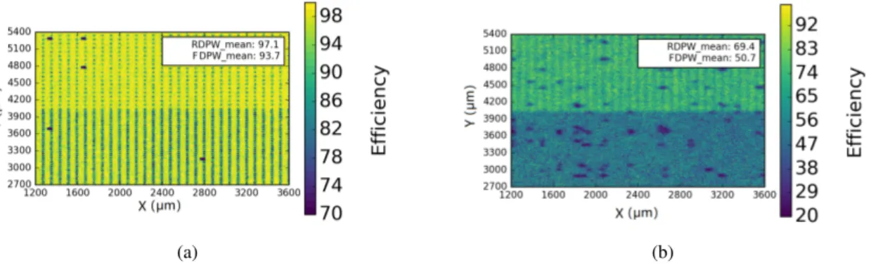
4.2.2 Efficiency
Figure7 shows the efficiency map measured with the 2.5 GeV electron beams at the ELSA facility, for an unirradiated chip and a neutron irradiated chip at 1015neq/cm2. For the unirradiated
chip, full efficiency was expected, but the measured mean detection efficiency is 97.1% in the region where deep pwell is partially removed (RDPW) and 93.7% in the region with deep pwell
PoS(Vertex2019)026
covering the full electronic area (FDPW). After irradiation, the efficiency drops significantly, down to 69.4% in the RDPW region and to 50.7% in the FDPW region. The higher efficiency measured for the RDPW region suggests that the shape of deep pwell may modulate the field lines towards the sensing node. Similar effects have also been observed in the MALTA chip sharing a similar sensor configuration as TJ-Monopix1 [7].
(a) (b)
Figure 7: Hit detection efficiency map of(a)an unirradiated and(b) a neutron irradiated (1015neq/cm2)
TJ-Monopix1 chip. The upper half of the matrix has the deep pwell partially removed (RDPW) and the lower half of the matrix has full deep pwell coverage (FDPW).
By projecting the efficiency into sub-pixel regions, low efficient corners have been observed in the unirradiated chip. Figure8 compares the in-pixel efficiency map of the unirradiated chip with a layout of 2 × 2 pixels. It can be seen that the low efficiency parts coincide with the pixel corners containing large-area active regions. For the other pixel corners, e.g. the center region in figure8(a), an efficiency as high as expected has been achieved. It is noted that the active region is isolated by thick field oxide and is formed before dopant implantation. The low dose N implant layer (see figure1(b)) might be deeper under those large active regions due to the absence of field oxide. Hence, it is suspected that a volume with localized minimum potential for electrons has been created under the low efficiency pixel corner because of the deeper N−implant, which leads to incomplete charge collection. In TJ-Monopix1, these large active regions are only used for filling structures as decoupling capacitors, and can be modified in the future in order to achieve a pixel design with uniformly distributed active regions.
The results obtained in this section indicate that the lateral collection field needs to be improved for high efficiency, especially after irradiation. This requires more careful pixel layout design as well as further sensor engineering. Two different technological fixes have been proposed based on TCAD simulation [18], and both of them have been proven to be effective for improving the lateral field substantially in later tests with another chip [19].
5. Conclusions
DMAPS devices in large format have already been established, making them readily available towards detector systems that may be very attractive for high-rate and high-radiation environments in future applications like the ATLAS experiment at HL-LHC. Our LFoundry DMAPS development line has followed the large electrode concept which is an intrinsically radiation hard design approach.
PoS(Vertex2019)026
DMAPS in the LFoundry 150 nm and TowerJazz 180 nm CMOS Technologies T. Wang
(a) (b)
Figure 8:(a)In-pixel efficiency projected into the 2 × 2 pixel region and(b)layout of 2 × 2 pixels containing
only the selected relevant layers. The results are taken from a sub-matrix with full deep pwell coverage (FDPW). The corners with low efficiency coincide with the corners containing large active area. The active region is typically used for implementing active devices like MOS transistors, and different active regions are isolated by thick field oxide.
The latest prototype called LF-Monopix1 is, to the authors’ knowledge, the first fully monolithic DMAPS design in the LFoundry technology that has demonstrated high sensor bias voltage with small leakage, full circuit functionality and high radiation tolerance to a particle fluence of at least 1015neq/cm2. Intensive R&D has also been performed on DMAPS design with a small electrode
in order to enhance the radiation tolerance, and important lessons have been learned with the prototypes in the TowerJazz 180 nm CMOS technology, pointing out the weakness of the current design and the path for future improvements. Technological fixes as well as design optimization for the small electrode design have been implemented in a small scale test chip called MiniMALTA in TowerJazz, which has already shown significant improvements in both sensor charge collection property and circuit performance [19]. The design of next-generation Monopix chips in the two mentioned technologies are on-going, both of which feature optimized analog front-end electronics, smaller pixels and larger sensor format than their ancestors. Technological fixes will also be implemented in the TowerJazz chip. The submission of these new chips is expected in early 2020.
Acknowlegements
This work has been supported in parts by the Deutsche Forschungsgemeinschaft (DFG) under grant number WE 976/4-1, the German Federal Ministry of Education and Research (BMBF) under grant number 05H15PDCA9, the H2020 project AIDA-2020 under GA no. 654168 and the H2020 project STREAM under GA no. 675587.
References
[1] R. Turchetta, J. Berst, B. Casadei, G. Claus, C. Colledani, W. Dulinski et al., A monolithic active pixel
sensor for charged particle tracking and imaging using standard VLSI CMOS technology,Nucl.
Instrum. and Meth.458 (2001) 677.
[2] G. Contin, The STAR PXL detector,J. Instrum.11 (2016) C12068.
PoS(Vertex2019)026
[3] M. Mager, ALPIDE, the monolithic active pixel sensor for the ALICE ITS upgrade,Nucl. Instrum.
and Meth.824 (2016) 434.
[4] T. Hemperek, Overview and perspectives of depleted CMOS sensors for high radiation environments,
Proc. Sci.309 (2018).
[5] T. Wang, P. Rymaszewski, M. Barbero, Y. Degerli, S. Godiot, F. Guilloux et al., Development of a depleted monolithic CMOS sensor in a 150 nm CMOS technology for the ATLAS inner tracker
upgrade,J. Instrum.12 (2017) C01039.
[6] T. Wang, M. Barbero, I. Berdalovic, C. Bespin, S. Bhat, P. Breugnon et al., Depleted fully monolithic CMOS pixel detectors using a column based readout architecture for the ATLAS inner tracker
upgrade,J. Instrm.13 (2018) C03039.
[7] L. S. Argemi, I. A. Asensi, I. Berdalovic, D. Bortoletto, R. Cardella, F. Dachs et al., The MALTA
CMOS pixel detector prototype for the ATLAS pixel ITK,Proc. Sci.348 (2019).
[8] H. Augustin, N. Berger, S. Dittmeier, F. Ehrler, C. Grzesik, J. Hammerich et al., Mupix8 — large area
monolithic hvcmos pixel detector for the mu3e experiment,Nucl. Instrum. and Meth.936 (2019) 681.
[9] M. Kiehn, A. Herkert, A. Weber, A. Schöning, A. Miucci, A. Fehr et al., Performance of the
ATLASPix1 pixel sensor prototype in ams aH18 CMOS technology for the ATLAS ITk upgrade,J.
Instrum.14 (2019) C08013.
[10] I. Peri´c, A novel monolithic pixelated particle detector implemented in high-voltage CMOS
technology,Nucl. Instrum. and Meth.A582 (2007) 876.
[11] M. Havránek, T. Hemperek, H. Krüger, Y. Fu, L. Germic, T. Kishishita et al., DMAPS: a fully depleted
monolithic active pixel sensor—analog performance characterization,J. Instrum.10 (2015) P02013.
[12] W. Snoeys, G. A. Rinella, H. Hillemanns, T. Kugathasan, M. Mager, L. Musa et al., A process modification for CMOS monolithic active pixel sensors for enhanced depletion, timing performance
and radiation tolerance,Nucl. Instrum. and Meth.871 (2017) 90.
[13] I. Peri´c, L. Blanquart, G. Comes, P. Denes, K. Einsweiler, P. Fischer et al., The FEI3 readout chip for
the ATLAS pixel detector,Nucl. Instrum. and Meth.A565 (2006) 178.
[14] M. Garcia-Sciveres, D. Arutinov, M. Barbero, R. Beccherle, S. Dube, D. Elledge et al., The FE-I4
pixel readout integrated circuit,Nucl. Instrum. and Meth.A636 (2011) S155.
[15] J. Liu, M. Barbero, S. Bhat, P. Breugnon, I. Caicedo, Z. Chen et al., Simulations of depleted CMOS
sensors for high-radiation environments,J. Instrum.12 (2017) C11013.
[16] D.-L. Pohl, T. Hemperek, I. Caicedo, L. Gonella, F. Hügging, J. Janssen et al., Radiation hard pixel
sensors using high-resistive wafers in a 150 nm CMOS processing line,J. Instrum.12 (2017) P06020.
[17] I. Mandi´c, V. Cindro, A. Gorišek, B. Hiti, G. Kramberger, M. Zavrtanik et al., Charge-collection
properties of irradiated depleted CMOS pixel test structures,Nucl. Instrum. and Meth.A903 (2018)
126.
[18] M. Munker, M. Benoit, D. Dannheim, A. Fenigstein, T. Kugathasan, T. Leitner et al., Simulations of CMOS pixel sensors with a small collection electrode, improved for a faster charge collection and
increased radiation tolerance,J. Instrum.14 (2019) C05013.
[19] M. Dyndal, V. Dao, P. Allport, I. A. Tortajada, M. Barbero, S. Bhat et al., Mini-MALTA: Radiation hard pixel designs for small-electrode monolithic CMOS sensors for the high luminosity LHC,