HAL Id: cea-02494007
https://hal-cea.archives-ouvertes.fr/cea-02494007
Submitted on 28 Feb 2020
HAL is a multi-disciplinary open access
archive for the deposit and dissemination of
sci-entific research documents, whether they are
pub-lished or not. The documents may come from
teaching and research institutions in France or
abroad, or from public or private research centers.
L’archive ouverte pluridisciplinaire HAL, est
destinée au dépôt et à la diffusion de documents
scientifiques de niveau recherche, publiés ou non,
émanant des établissements d’enseignement et de
recherche français ou étrangers, des laboratoires
publics ou privés.
Hybrid Prototyping Methodology for Rapid System
Validation in HW/SW Co-Design
Arief Wicaksana, Amir Charif, Caaliph Andriamisaina, Nicolas Ventroux
To cite this version:
Arief Wicaksana, Amir Charif, Caaliph Andriamisaina, Nicolas Ventroux.
Hybrid Prototyping
Methodology for Rapid System Validation in HW/SW Co-Design. The Conference on Design and
Architectures for Signal and Image Processing 2019 (DASIP 2019), Oct 2019, Montreal, Canada.
�cea-02494007�
Hybrid Prototyping Methodology for Rapid System
Validation in HW/SW Co-Design
Arief Wicaksana, Amir Charif, Caaliph Andriamisaina and Nicolas Ventroux
CEA, List, Embedded Computing Laboratory 91191 Gif-sur-Yvette CEDEX, France
Abstract—As the System-on-Chip (SoC) complexity increases, hardware/software co-design plays an important role to improve design productivity, reduce time to market, and optimize the overall results. Consequently, there is a high interest in providing rapid system validation in such a paradigm to achieve the aforementioned objectives. There exist in previous works proto-typing techniques related to the development phase. FPGA-based prototyping has the benefits of enabling HW/SW integration and system validation after the Register Transfer Level (RTL) implementation is available while virtual platforms provide capabilities to accelerate software development with higher level functional models, e.g. Transaction Level Modeling (TLM).
In this paper, we propose a hybrid prototyping methodology which takes advantage of virtual and FPGA-based prototyping in a single framework. We aim to provide a rapid and flexible system validation solution for HW/SW co-design at various stages of development based on the availability of TLM and RTL implementations. The proposed methodology allows online and offline performance analysis and debugging for early feedback in HW/SW architecture exploration. This was evaluated in the experiments with a neural network processor as a case study.
Index Terms—hybrid prototyping, rapid system validation, HW/SW co-design
I. INTRODUCTION
System-on-Chip (SoC) architects nowadays are facing greater challenges in development due to the ever-increasing size and complexity of SoC design. Hardware architectures and the software stacks that drive them need to be validated together for higher productivity and reduced time to market. Unfortunately, the traditional development process allows inte-grating and validating hardware/software (HW/SW) only after hardware development is finished and the first silicon samples are available [1]. To overcome such a limitation, various techniques in HW/SW co-design with or without hardware models were proposed [2]. Each technique differs from the others in terms of simulation speed, debugging capability, HW/SW availability, etc.
For years, Field-Programmable Gate Array (FPGA) has been targeted in physical prototyping to validate systems based on their Register Transfer Level (RTL) implementations. It provides accuracy and execution speed close to the real operation. However, FPGA-based prototypes do not offer the same level of visibility and control over the design compared to simulation and emulation environments [3]. Furthermore, software and hardware designs can only be deployed in FPGA after the RTL implementations are ready.
Virtual prototyping, on the contrary, offers a simulation environment before RTL implementations are available. It allows SoC architects to start software development earlier,
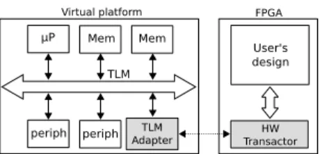
TLM µP Mem
TLM Adapter
Virtual platform FPGA
HW Transactor User's design Mem periph periph
Fig. 1:Typical system built on a hybrid prototyping framework
thereby shortening the overall schedule. Virtual prototyping uses SystemC/TLM [4] as the de facto standard to model sys-tem architecture with different simulation speeds and accuracy levels. Despite that, the performance of a virtual platform when building simulation environments close to the real application is impacted by the degree of the complexity of the models.
This paper presents a hybrid prototyping methodology for rapid system validation in HW/SW co-design. It combines the strength of virtual and FPGA-based prototyping in a single validation framework. Figure 1 describes a typical system built using such a methodology. Our work enables rapid HW/SW integration and system validation in SoC development by pro-viding prototyping solutions at various stages of development based on the availability of TLM and RTL implementations. As a result, SoC architects (users) are granted with an opti-mized and flexible validation flow as well as the possibility of incremental architecture explorations.
We propose a new method for integrating FPGA prototyping and virtual prototyping approaches. For this purpose, both virtual and physical prototypes are executed concurrently in the framework and synchronized every quantum as per a loosely timed model in TLM. A TCP-based connection is used to allow seamless communication and flexible FPGA implementation. As a result, the use of locally-connected and remote FPGAs is possible within our solution. Besides the validation results, the methodology also provides performance analysis and debugging features which are important in valida-tion iteravalida-tions. Component statistics from virtual and physical prototypes are accessible from a unified debugging interface. Furthermore, this interface also enables to use breakpoints and logic analyzers in the FPGA to perform runtime analysis.
The remainder of this paper is organized as follows. Sec-tion II presents a review of some related works. SecSec-tion III describes the proposed system validation flow using our hybrid prototyping solution. Section IV details the hybrid prototyping framework and its features. Section V presents the experiments with a case study of neural network processor validation. Finally, Section VI presents the conclusion and perspectives.
II. RELATEDWORKS
Co-simulation solutions based on virtual prototyping have been proposed to provide system validation using Sys-temC/TLM models. An example of a co-simulation framework which targets multi-processors system on chip (MPSoC) is presented in [5]. The processor is modeled in a set of In-struction Set Simulators (ISS) that executes the SW parts of the system while the hardware is described in SystemC. As their model is cycle-accurate, it offers visibility close to RTL simulation but with a very slow performance. Other works propose to use a processor emulator such as QEMU to provide an accurate and realistic CPU model [6, 7]. The integration of QEMU to emulate the processors and TLM to model the hardware modules results in a fast co-simulation method in exchange for cycle accuracy.
Both higher performance and cycle accuracy in validation can be obtained by integrating FPGA-based emulation [8, 9]. In [8], a C/C++ simulator models the processors and an FPGA emulates their peripherals. This offers a high verifica-tion accuracy and full synchronizaverifica-tion between simulator and FPGA thanks to its shared register communication. However, the FPGA utilization in [8] is non-optimal due to the costly synchronization from the C/C++ simulator every clock cycle. The work in [9] presents a combination of different abstraction levels to emulate the entire system in FPGA-based prototyp-ing. Embedded microprocessors in FPGA are used to run TLM models while RTL modules are mapped in the reconfigurable logic arrays. The communication overhead between TLM and RTL is reduced since they run on the same platform. However, this solution consumes significant FPGA resources and limits the SoC design that can be fitted inside the FPGA.
An accurate and much more rapid validation can be achieved by FPGA-based prototyping [3]. It allows a large number of verification cycles running at speed much closer to real time. Despite that, FPGA prototypes lack visibility and control over the design compared to simulation and emulation environments. To overcome such limitations, many works have been done to add debugging capabilities in FPGA. Logic analyzers [10, 11] are provided by FPGA vendors to monitor internal signals inside the FPGA in exchange for a significant amount of memory resources. The work in [12] presents an internal node probing methodology to dump out signal activities from FPGAs during co-simulation. However, this solution requires extensive modification from initial RTL designs to integrate the probes. [13] presents a less intrusive method using an FPGA-based trace module to monitor internal signals and provide activity events, such as the number of executed instructions and RAM read/write accesses.
The use of virtual prototyping complemented by FPGA prototyping is by far showing the highest potential in system validation. Such a combination is presented in [14–16]. The work in [14] uses a cycle-accurate virtual platform simulator and IPC (Inter-Process Communication) to communicate with physical prototypes. [15] shows a platform that integrates functional simulation and an FPGA for HW/SW verification. HAPS [16] offers a possibility of using the cycle-accurate virtual prototyping tool from Synopsys with TLM interface to manipulate the hardware platform.
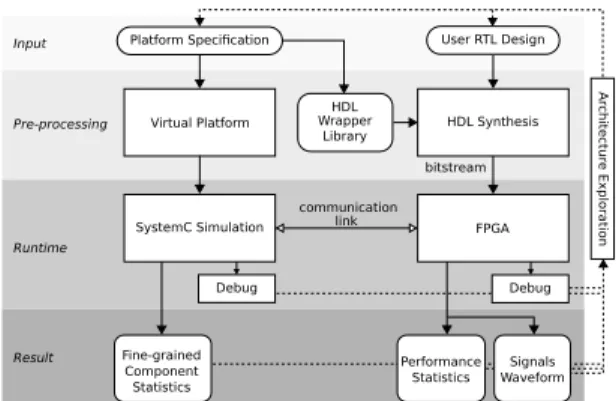
Platform Specification User RTL Design
Virtual Platform
SystemC Simulation FPGA
HDL Synthesis bitstream Wrapper Library HDL Input Pre-processing Runtime communication link Fine-grained Component Statistics Debug Result Ar chitec tur e Exploration Signals Waveform Performance Statistics Debug
Fig. 2: System validation flow provided by our hybrid prototyping
solution
Our hybrid prototyping solution is distinct from the existing works in that it uses a loosely-timed model in the virtual plat-form. The virtual and physical prototypes can concurrently run and synchronize whenever a communication occurs to reduce the overhead. We also provide a flexible implementation of the FPGA thanks to the light TCP-based communication. Finally, our solution supports runtime debugging and performance analysis for both virtual and FPGA-based prototypes.
III. HW/SW VALIDATIONOVERVIEW
We propose a system validation methodology for HW/SW co-design using a hybrid prototyping framework. This method-ology takes advantage of both virtual and FPGA-based pro-totyping to validate HW/SW architectures. Figure 2 depicts the validation flow provided in our framework. The proposed framework takes as an input a platform specification which describes the full system architecture and software stacks. It also takes the user’s RTL design for the parts that need to be validated as prototypes in FPGAs. As the output, HW/SW validation results and performance statistics of each component are generated by the framework.
The virtual platform in our framework uses the provided specification to build the system architecture from Sys-temC/TLM models and to include software binaries. Then, the platform is simulated using SystemC. Meanwhile, the specification also describes a communication wrapper which is implemented as a HW transactor in the FPGA platform. The wrapper and the user’s design are then synthesized together to generate a configuration file (bitstream) for the targeted FPGA. Afterwards, both the virtual and FPGA-based prototypes are concurrently executed. During execution, our hybrid frame-work allows users to debug on specific parts of execution both in the virtual platform and FPGA using breakpoint addresses. The detail of this feature will be explained in Section IV. The runtime debug feature has shown to be very useful in multiple iterations for rapid HW/SW validation.
Furthermore, the proposed framework offers not only rapid system validation results, but also performance statistics which can be used to find errors and optimize the system architecture. The activity report of each component, whether they be virtual or physical is accessible from a unified interface during valida-tion. This interface is provided by the virtual prototyping tool used in our framework. It allows users to extract fine-grained component statistics from SystemC simulation for online and
offline analysis, and design statistics from the FPGA through the communication link. This communication link is built from the virtual platform’s interface and the wrapper added in the FPGA. The statistics in the FPGA record the performance of validated designs, e.g. read/write events, read/write cycles, etc. For a more thorough offline analysis, the wrapper in the FPGA enables internal signal monitoring and recording. The selection process of signals should be done before the synthesis while the recording process can be controlled by users at runtime.
The high complexity of modern SoC demands hardware and software parts to be developed and validated together in a condition close to the real application. The proposed hybrid prototyping methodology is able to address this challenge. For instance, developing a Linux driver for a new peripheral device requires access to specific library and functions. The use of vir-tual platform enables functional and compatibility verification of this driver directly on the targeted operating system. The FPGA integration in the framework allows reusing stable IPs or incrementally adding new IPs to the architecture. As more SoCs integrate accelerators, the proposed hybrid prototyping framework can be an excellent tool in the development of such a system. The presented methodology can be used throughout development of complex systems, from the early stage where the entire system is described only in functional models until the final prototyping stage before manufacturing. Moreover, most parts of the flow presented in Figure 2 are automated and users only need to deal with providing the platform specification and RTL design. The next section will detail our hybrid prototyping framework and its features.
IV. HYBRIDPROTOTYPINGFRAMEWORKARCHITECTURE
Firstly, we will present the virtual prototyping solution used in this work. Then, we will detail the communication architecture between the virtual platform and the FPGA which enables them to simulate a common system. Finally, we will describe some features for debugging and performance analysis in rapid system validation provided by our framework. A. Virtual Prototyping Tool
In this work, the virtual platform is built using VPSim [7]. VPSim is an existing tool, part of the SESAM EDA frame-work, which is used for virtual prototyping and Design Space Exploration (DSE). As a virtual prototyping tool, VPSim is based on SystemC/TLM simulation. And thanks to its efficient implementation of loosely-timed TLM models, it exhibits a very high speed in HW/SW validation. VPSim includes a large library of CPUs, buses and peripheral models that can be used to build the required SoC architecture. It is also capable of integrating third-party SystemC/TLM models and external FMI systems as proxy components.
The strength of using VPSim lies especially in its ability to perform dynamic configuration of the modeled platform. VP-Sim only requires a single compilation at the beginning and is able to dynamically instantiate the platform before simulation. This gives a high flexibility in architecture exploration during iterative validation scenarios. Another advantage brought by VPSim is that it enables users to perform architecture profiling and performance analysis. Once the simulation is launched, it gathers each component activity and provides fine-grained
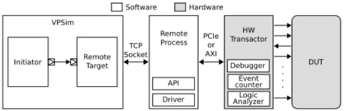
DUT Debugger Event counter Logic Analyzer HW Transactor Remote Process PCIeor AXI TCP Socket Software Hardware
Initiator RemoteTarget
API Driver VPSim
Fig. 3:Communication between VPSim and FPGA in the Proposed
Hybrid Prototyping Framework
statistics. These statistics can be viewed either during runtime via VPSim’s built-in debug and profiling utility or at the end of simulation.
In this work, the VPSim’s built-in debug and profiling utility is used as a unified interface for debugging both the virtual platform and the FPGA. At runtime, users can halt the entire execution and enter an interactive mode. In this mode, performance statistics at the current time can be extracted from each component in the validated system. Furthermore, the debugging interface allows users to create breakpoints in the FPGA prototype. The start and end of the signal monitoring process are also controlled from this interface.
B. Communication between Virtual – FPGA Prototype In addition to the rich component library offered by VPSim, a feature that connects the virtual platform and the design under test (DUT) in FPGAs is necessary in our framework. From VPSim’s point of view, the DUT in FPGAs is considered as a TLM remote target. Remote target is a proxy component that connects VPSim to external prototyping devices, such as RTL simulators or FPGAs. Figure 3 describes a logical representation of the connection between VPSim and a DUT in FPGAs. When a TLM initiator, such as a CPU, needs to access a peripheral device or accelerator in FPGAs, it communicates with an instantiated remote target inside VPSim. The remote target is connected to an external remote process via a TCP socket. Thanks to the communication using TCP socket, connecting VPSim to a remote FPGA via Ethernet network is also possible. The remote process then forwards read/write accesses from the TLM initiator to the HW Transactor through a PCIe or AXI interconnect. Finally, the HW Transactor will perform read and write operation with the DUT based on the access requests from TLM initiator.
In contrast with the existing works [14, 16] which directly connect the TLM target to the HW Transactor in FPGAs, we propose to create a remote process between them. Combined with the TCP socket used in the communication, our frame-work gives freedom in connecting the FPGA resources and sharing them among users. It enables to use either locally connected or remote FPGAs. Another reason is to allow a utilization of multiple FPGA resources in the prototyping. As the number of PCIe/AXI connection that a PC can provide is limited, expensive prototyping platforms use an FPGA as a router to the other FPGAs in the system. We provide a possibility of using several smaller FPGAs connected to the virtual platform. As more SoC-FPGA platforms with server-like performance are becoming available in the market, our solution will provide better flexibility and scalability.
The virtual platform in our proposed hybrid prototyping framework uses a loosely-timed model for the SystemC/TLM
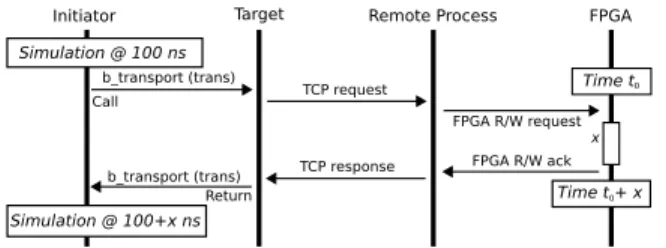
Target
b_transport (trans) Call
Return
Initiator Remote Process
b_transport (trans) FPGA TCP request TCP response FPGA R/W request FPGA R/W ack x Simulation @ 100+x ns Simulation @ 100 ns Time t0 Time t + x0
Fig. 4: Communication between VPSim simulation and FPGA
execution in the proposed framework
Algorithm 1 VPSim – FPGA communication mechanism
procedure FPGATRANSPORT
FPGATime← getFpgaTime() if req = READ then
readF pga() else if req = WRITE then
writeF pga()
return (getFpgaTime() − FPGATime)
simulation. The communication between TLM initiators and targets is therefore blocking. We apply this blocking com-munication to the FPGA-based prototype to ensure consistent behavior during overall validation. The execution in VPSim and in the FPGA run in parallel over a certain duration and perform a synchronization during the communication.
The communication mechanism between the virtual plat-form and the FPGA is depicted in Figure 4. When using a loosely-timed model in SystemC, the simulation of TLM initiators and targets proceeds at every quantum. We extend this approach for the synchronization between VPSim and the FPGA in the proposed framework. The time spent by the FPGA to handle the request is calculated in the VPSim simulation time. It is extracted from the FPGA each time a communication occurs. During a read/write request, a TLM
initiator calls b_transport on a target socket. This call
triggers a TCP request to the remote process which is located outside of VPSim, leading to a R/W request on the FPGA prototype. After the FPGA handles the request, it sends an acknowledgment signal to the remote process, which will be forwarded to the TLM target, and finally returns from the
call to b_transport. The FpgaTransport procedure in
Algorithm 1 shows how the remote process performs a R/W request and extracts the real execution time.
The FPGA execution proceeds at every quantum, just like a TLM module. We add a SystemC thread in VPSim to trigger a ’step’ in the FPGA and put it into a ’sleep’ mode in order to let other threads proceed in the simulation. The FPGA execution will continue for a quantum and will be blocked until the next trigger is received from the SystemC thread. Hence, the execution of VPSim and the FPGA run in parallel with each local quantum while being synchronized to a global simulation time. It is worth noting that the FPGA timing can be decoupled from the rest of the system to obtain higher performance in functional validation where time accuracy is not necessary. C. Run-Time Performance Analysis and Debug
In contrast to RTL simulation and emulation, FPGA-based prototyping does not offer detailed information regarding circuit activity. Consequently, the ability to perform runtime
performance analysis and debugging is limited in FPGA-based prototypes. Nevertheless, there are some basic features which can be added in rapid verification or validation without incurring a significant penalty to the validation performance. As presented in Figure 3, the HW Transactor wraps the DUT and supports the communication with TLM models in VPSim. In addition to this functionality, we integrate the following capabilities to offer higher design visibility and control in system validation.
1) Performance Counter
Performance counters are integrated to measure the number of read/write operations, read/write cycles, read/write bandwidth, and access to addresses. These counters monitor bus activities connected to the DUT and summarize data activity into a simple statistics report. The performance counters work throughout vali-dation except for number of access counters which must be controlled from the VPSim debugging interface. 2) Breakpoint Debugger
Our framework allows users to assign breakpoint ad-dresses to the FPGA through VPSim’s interface at runtime. When there is any activity (read or write) to a breakpoint address, the execution in VPSim and the FPGA will freeze at the exact moment. From this point, users may send a command to show performance statistics in the FPGA, and view the component states and CPU registers, check the memory contents, etc. in VPSim. They can also add another breakpoint and resume the execution.
3) Logic Analyzer
The ability to precisely monitor signal activities has proven to be compelling especially during HW valida-tion. We include a configurable logic analyzer inside the HW Transactor to monitor more detailed activity in the FPGA. Selected signals in the FPGA are recorded during prototyping. The signal selection is done inside the HW Transactor before synthesis. To minimize hard-ware overhead that may reduce FPGA performance, the recorded signal activities are flushed and dumped to a VCD file. The start and end of recording is controlled from the debugging interface of VPSim.
V. CASESTUDY
To evaluate our hybrid prototyping methodology, we con-sidered a case study of HW/SW validation during a SoC devel-opment. The objective was to validate a real image processing application which used deep neural network methodology. A neural network IP core was built to provide high-performance image classification in the system. Using the proposed hybrid prototyping methodology, we performed the experiments to validate the IP and software stacks that drive it.
A. Framework Setup
The setup was built using a PC and a remote server which contained an FPGA resource. The PC has 8 cores of Intel i7 @ 3.4 GHz and 16 GB of DDR memory. It runs 64-bit Linux Ubuntu 16.04 LTS as its operating system and has VPSim installed for virtual prototyping. The remote server has 8 cores of Intel Xeon @ 2.67 GHz and 16 GB of DDR memory. It runs
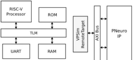
RISC-V Processor ROM RAM AXI Bus PNeuro IP TLM VPSim R emoteT ar get UART
Fig. 5:Architecture with RISC-V and PNeuro IP
64-bit Red Hat Enterprise Linux 7. In addition, the server is connected with an FPGA prototyping platform via PCIe.
Due to availability reasons, we used the ProFPGA duo V7 platform [17] from proDesign to provide the FPGA resource in the server. ProFPGA duo V7 is a modular pro-totyping platform with a possibility of integrating multiple FPGAs and various supporting modules. In this work, we only used a single XC7V585T FPGA module. It integrates XC7V585T-1FFG1761 from Xilinx Virtex-7 family which contains 582 Klogic cells, 29 Mbits of block memory, 1260 DSP slices, etc. The connection between the FPGA and the PC server use a 4-lane PCIe Gen 2 which can offer up to 4 GB/s theoretical bandwidth. It is worth noting that the communication between VPSim and the FPGA is light and generic which allows a utilization of other commercial FPGAs. With the increasing popularity of MPSoC-FPGA platforms, e.g. Zynq Ultrascale+, the remote server can be replaced with such platforms by adapting the API and drivers used. B. HW/SW Validation Environment
For this case study, we used the framework to validate the PNeuro IP [18] and its software stacks. PNeuro is an IP devel-oped to accelerate deep neural network (DNN) applications, e.g. image classification. It is a neural network processor which can be programmed with 32-bit instructions for both control and computing. The SIMD clusters of PNeuro allows it to perform all the operations required in DNN (convolutions, pooling, non-linear functions, etc.) in parallel.
In a real-life scenario, accelerator such as PNeuro IP is provisioned for machine learning tasks while the rest of execution and system control is executed by general pur-pose processors. In the targeted architecture, this role of the general purpose processor is assigned to a multi-core RISC-V processor. Figure 5 presents the hardware architecture of the validated system. Besides the RISC-V and PNeuro, the architecture integrates a RAM, a ROM, and a UART controller for peripheral devices. For the software part, the global application which accesses PNeuro is executed by the RISC-V processor.
In the experiments, components can be allocated both in the virtual platform and in the FPGA according to the required accuracy and model availability. The PNeuro IP was synthe-sized and programmed in the FPGA to validate its hardware architecture. Meanwhile, we modeled the RISC-V processor, memories (RAM and ROM), and UART controller in VPSim. The image processing software that used PNeuro was also loaded in the RAM for the validation process. The remote target, remote process and HW Transactor (cf. Figure 3) are represented as VPSim remote target in Figure 5. To adapt to PNeuro’s input/output ports, the HW Transactor implements
TABLE I:Resource Utilization in the FPGA (Place-and-Route)
LUT FF BRAM HW Transactor 2806 2956 1* PNeuro 73716 11308 66 Overhead +3.8% +26.1% N/A
*For each 32-bit data record during 1024 cycles
the AXI4 interface. The working frequency of the design inside FPGA is fixed at 100 MHz.
Table I presents the resource utilization in the FPGA. HW Transactor and PNeuro IP were synthesized using Vivado Design Suite 2018.2. The logic and register utilization of HW transactor in FPGA are relatively constant as they do not depend on the validated systems. They take less than 1% of the used resource in the FPGA. When being compared to PNeuro IP, the HW Transactor generates 3.8% overhead in logic utilization which is relatively small. The register overhead is 26.1% due to the resource required for storing the configuration of event counters, breakpoint, and signal monitoring infrastructure.
BRAMs are required in HW transactor to temporarily record signal activities before being dumped to a VCD file. The amount of BRAM needed in the framework is linear to the number of signals probed and how often the data are dumped out. We found that 1 BRAM was required to record 32-bit data during 1024 cycles. Our framework uses 5 BRAMs at a minimum to monitor AXI4 channels in the experiments. In case of a larger quantum in the FPGA prototype, the amount of used BRAMs in the HW Transactor will increase.
C. Experimental Results
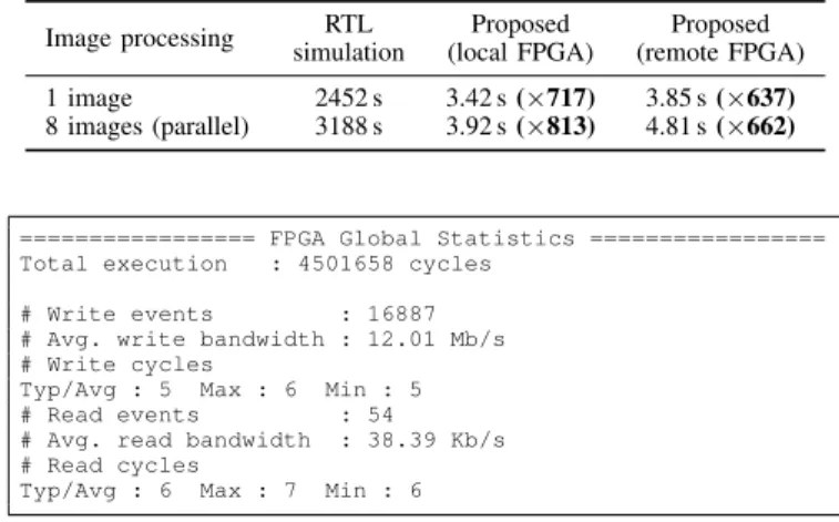
In the experiments, we ran two applications on the PNeuro IP for HW/SW validation: classification of 1 image and 8 images in parallel. The former application executed 379894 instructions while the latter executed 454153 instructions. The higher number of instructions in the second application is due to more image transfers between the RAM and PNeuro. For comparison purposes, we also validated the system using the proposed framework with a locally-connected FPGA, and in RTL simulator Questa 10.6 by Mentor Graphics [19]. To locally connect VPSim and the FPGA, we installed VPSim in the remote server (cf. Section V-A).
Table II shows the comparison of validation time using the proposed hybrid prototyping framework and a RTL simulation. The RTL simulation only dumps the AXI4 interface signals for minimum observation and faster execution. Even so, we can see from the table that the proposed hybrid prototyping methodology results in a much faster (at least 637 times) val-idation process compared to RTL simulation. In our solution, the use of remote FPGAs adds a small overhead compared to local FPGAs due to the delay in Ethernet communication. Hence, this overhead increases with communication between VPSim and the FPGA. In these experiments, the processor RISC-V was pooling the results from PNeuro throughout validation which presented an unfavorable condition in the communication. The performance comparison with other hy-brid prototyping solutions is unavailable due to few equivalent system-level validation results in the literature.
TABLE II: PNeuro validation time comparison
Image processing simulationRTL (local FPGA)Proposed (remote FPGA)Proposed 1 image 2452 s 3.42 s (×717) 3.85 s (×637) 8 images (parallel) 3188 s 3.92 s (×813) 4.81 s (×662)
================= FPGA Global Statistics =================
Total execution : 4501658 cycles
# Write events : 16887
# Avg. write bandwidth : 12.01 Mb/s # Write cycles
Typ/Avg : 5 Max : 6 Min : 5
# Read events : 54
# Avg. read bandwidth : 38.39 Kb/s
# Read cycles
Typ/Avg : 6 Max : 7 Min : 6
Fig. 6:FPGA statistics report at the end of HW/SW validation
Both VPSim and the FPGA produces performance statistics which can be shown at runtime via VPSim debug interface or in a report at the end of HW/SW validation. Figure 6 depicts an example of the statistics report produced for the FPGA. The statistics in the FPGA are produced by the performance counters in HW Transactor. It shows R/W events, average bandwidth, and cycle required to perform a single read/write by DUT. Similarly, VPSim also generates a report of read/write count, instructions count, etc. from SystemC simulation.
Another feature tested during validation is the logic analyzer which monitors FPGA internal signals. Figure 7 presents the output of AXI4 bus signal monitoring exported to a waveform in gtkwave tool. As explained in Section IV, the provided signal monitoring has a very small impact on the validation performance. However, our current implementation sequentially dumps signals into a file for every monitored signal, which is not optimized. This is frequently performed to reduce BRAM utilization which decreases validation speed. It took 55.81 s to monitor the entire validation at a minimum amount of BRAMs and it generated a VCD file with a size of 434 MB. In future works, this monitoring implementation can be improved with a scan-chain methodology presented in [20] or statistical sampling method [21].
VI. CONCLUSIONS
We present a hybrid prototyping methodology to provide a rapid system validation in HW/SW co-design. This method-ology merges a fast HW/SW validation provided by virtual prototyping with a rapid and accurate hardware verification by FPGA. It offers the ability to validate both software and hardware designs in various stages of SoC development, from high-level functional description to RTL implementations. In
Fig. 7:Real-time AXI4 bus monitoring results shown in gtkwave
this work, the hybrid prototyping solution is based on VPSim and a commercial FPGA locally or remotely connected.
The proposed solution is capable of generating performance statistics reports from both VPSim and FPGA executions. These statistics can be accessed in the middle or at the end of validation iterations. In addition, we add runtime debugging feature which uses breakpoint addresses to freeze execution and perform a thorough analysis at runtime. For signal monitoring in FPGA, a logic analyzer is provided for offline analysis. In future works, we are looking forward to increasing communication and monitoring speed, and to add physical statistics during validation, such as dynamic power consumption. Further measurements with High-Level Synthesis (HLS) benchmark applications are also considered.
REFERENCES
[1] Soonhoi Ha and Jrgen Teich. Handbook of Hardware/Software Codesign. Springer Publishing Company, Incorporated, 2017.
[2] James A Rowson. Hardware/Software Co-simulation. In 31st Design Automation Conference, pages 439–440. IEEE, 1994.
[3] Nitin Gupta and Chethan Harakchand. Embracing the FPGA Challenge for Processor Design Verification. In 2014 15th International Microprocessor Test and Verification Workshop, pages 39–43. IEEE, 2014.
[4] John Aynsley et al. OSCI TLM-2.0 Language Reference Manual. Open SystemC Initiative, 24, 2009.
[5] Stefano Cordibella, Franco Fummi, Giovanni Perbellini, and Davide Quaglia. A HW/SW Co-simulation Framework for the Verification of Multi-CPU Systems. In High Level Design Validation and Test Workshop, 2008. HLDVT’08. IEEE International, pages 125–131. IEEE, 2008.
[6] Marius Monton, Antoni Portero, Marc Moreno, Borja Martinez, and Jordi Carra-bina. Mixed SW/SystemC SoC Emulation Framework. In Industrial Electronics, 2007. ISIE 2007. IEEE International Symposium on, pages 2338–2341. IEEE, 2007. [7] Amir Charif, Gabriel Busnot, Rania Mameesh, Tanguy Sassolas, and Nicolas Ventroux. Fast Virtual Prototyping for Embedded Computing Systems Design and Exploration. In 11th Workshop on Rapid Simulation and Performance Evaluation: Methods and Tools, 2019.
[8] Yuichi Nakamura, Kouhei Hosokawa, Ichiro Kuroda, Ko Yoshikawa, and Takeshi Yoshimura. A Fast Hardware/Software Co-verification Method for System-on-a-Chip by using a C/C++ Simulator and FPGA Emulator with Shared Register Communication. In Proceedings of the 41st annual Design Automation Conference, pages 299–304. ACM, 2004.
[9] Nobuyuki Ohba and Kohji Takano. An SoC Design Methodology using FPGAs and Embedded Microprocessors. In Proceedings of the 41st annual Design Automation Conference, pages 747–752. ACM, 2004.
[10] Xilinx Inc. ChipScope Integrated Logic Analyzer (ILA). https://www.xilinx.com/ products/intellectual-property/chipscope ila.html.
[11] Intel FPGA Inc. Quartus SignalTap II Logic Analyzer. https://www.intel.com/ content/dam/www/programmable/us/en/pdfs/literature/ug/signal.pdf.
[12] Sangjun Yang, Heejun Shim, Wooseung Yang, and Chong-Min Kyung. A new RTL Debugging Methodology in FPGA-based Verification Platform. In Proceedings of 2004 IEEE Asia-Pacific Conference on Advanced System Integrated Circuits, pages 180–183. IEEE, 2004.
[13] Guillaume Patrigeon, Pascal Benoit, and Lionel Torres. FPGA-based platform for fast accurate evaluation of Ultra Low Power SoC. In 2018 28th International Sym-posium on Power and Timing Modeling, Optimization and Simulation (PATMOS), pages 123–128. IEEE, 2018.
[14] Dionysios Diamantopoulos, Efstathios Sotiriou-Xanthopoulos, Kostas Siozios, George Economakos, and Dimitrios Soudris. Plug&Chip: A Framework for Supporting Rapid Prototyping of 3D Hybrid Virtual SoCs. ACM Transactions on Embedded Computing Systems (TECS), 13(5s):168, 2014.
[15] Zheng Zheng, Xinan Wang, Zhaoyang Guo, and Guoxing Zhang. An auto-matic software/hardware verification platform prototype for reconfigurable audio algorithm in media soc. In 2015 IEEE 11th International Conference on ASIC (ASICON), pages 1–4. IEEE, 2015.
[16] Synopsys Inc. HAPS Prototyping Solutions. https://www.synopsys.com/ verification/prototyping/haps.html.
[17] ProDesign Inc. ProFPGA duo Motherboard. https://www.profpga.com/products/ motherboards-overview/profpga-duo-.
[18] Alexandre Carbon, J-M Philippe, Olivier Bichler, Renaud Schmit, Benoˆıt Tain, D Briand, Nicolas Ventroux, Michel Paindavoine, and Olivier Brousse. PNeuro: A scalable energy-efficient programmable hardware accelerator for neural networks. In 2018 Design, Automation & Test in Europe Conference & Exhibition (DATE), pages 1039–1044. IEEE, 2018.
[19] Mentor Graphics Inc. Questa Advanced Simulator. https://www.mentor.com/ products/fv/questa/.
[20] X Cheng, AW Ruan, YB Liao, P Li, and HC Huang. A Run-Time RTL Debugging Methodology for FPGA-based Co-simulation. In 2010 International Conference on Communications, Circuits and Systems (ICCCAS), pages 891–895. IEEE, 2010. [21] Roland E Wunderlich, Thomas F Wenisch, Babak Falsafi, and James C Hoe. Statistical Sampling of Microarchitecture Simulation. ACM Transactions on Modeling and Computer Simulation (TOMACS), 16(3):197–224, 2006.