HAL Id: cea-01973705
https://hal-cea.archives-ouvertes.fr/cea-01973705
Submitted on 8 Jan 2019
HAL is a multi-disciplinary open access
archive for the deposit and dissemination of
sci-entific research documents, whether they are
pub-lished or not. The documents may come from
teaching and research institutions in France or
abroad, or from public or private research centers.
L’archive ouverte pluridisciplinaire HAL, est
destinée au dépôt et à la diffusion de documents
scientifiques de niveau recherche, publiés ou non,
émanant des établissements d’enseignement et de
recherche français ou étrangers, des laboratoires
publics ou privés.
Carrier scattering by workfunction fluctuations and
interface dipoles in high-κ/metal gate stacks
Zaiping Zeng, Francois Triozon, Yann-Michel Niquet
To cite this version:
Zaiping Zeng, Francois Triozon, Yann-Michel Niquet. Carrier scattering by workfunction fluctuations
and interface dipoles in high-κ/metal gate stacks. 2016 International Conference on Simulation of
Semiconductor Processes and Devices (SISPAD 2016), Sep 2016, Nuremberg, Germany.
�10.1109/SIS-PAD.2016.7605223�. �cea-01973705�
Carrier scattering by workfunction fluctuations and
interface dipoles in high-
κ
/metal gate stacks
Zaiping Zeng
∗†, Franc¸ois Triozon
‡†and Yann-Michel Niquet
∗†§∗CEA, INAC-MEM, L Sim, Grenoble, France †University Grenoble Alpes
‡CEA, LETI-MINATEC, Grenoble, France §Email: [email protected]
Abstract—The introduction of a high-κ/metal gate stack in metal-oxide-Semiconductor field-effect transistors can cause a significant degradation of the mobility, especially at weak in-version densities. This degradation is commonly ascribed to remote Coulomb scattering (RCS, i.e., charges trapped at the SiO2/HfO2 interface). However, very large densities of RCS
charges are usually needed to reproduce the experimental data. In this work, we explore alternative scattering mechanisms by quantum calculations of the carrier mobilities. We consider, in particular, metal grain workfunction fluctuations and local dipoles at the SiO2/HfO2 interface. Similarly to RCS, both
scattering mechanisms are found to reduce the carrier mobility significantly at low carrier densities. However, the mobility exhibits a different dependence on the thickness of high-κ layer, which provides a way to identify the dominant mechanism.
I. INTRODUCTION
High-κ/metal gate stacks have been introduced in Metal-Oxide-Semiconductor Field-Effect-Transistors (MOSFETs) in order to keep a tight electrostatic control over short channels while limiting gate leakage currents. However, they are re-sponsible for a significant degradation of the carrier mobilities, especially at weak inversion densities. A number of scattering mechanisms have been put forward to explain this degradation, such as remote Coulomb scattering (RCS, i.e., charges trapped at the SiO2/HfO2 interface). However, the density of RCS
charges needed to reproduce the experimental mobilities is usually very high (a few 1013 cm−2 [1], [2]), and shall result in significant threshold voltage shift and variability. Therefore, we explore in this work alternative mechanisms, such as granularity in the metal gate and local dipoles at the SiO2/HfO2 interface, using quantum calculations in the
non-equilibrium Green’s Functions (NEGF) framework. NEGF al-lows a straightforward, explicit introduction of such disorders in the geometry of the devices.
II. METHODOLOGY AND DEVICES
The simulated devices are (100) fully-depleted silicon-on-insulator (FDSOI) transistors with film thickness tSi= 4 nm
and width W = 60 nm. The transport properties are computed in the non-equilibrium Green’s function (NEGF) framework. We focus on electrons, described within the effective-mass ap-proximation. The NEGF equations are solved self-consistently
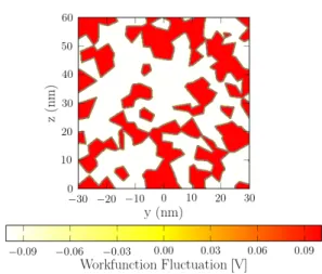
Fig. 1. An example of metal grain pattern in a L = 60 nm × W = 60 nm device with an average grain diameter D = 5 nm. The workfunction fluctuation is plotted in each grain at the metal/HfO2 interface. Each grain
has a probability p = 0.4 to have a workfunction WF = 4.4 eV (i.e., ∆WF = −0.1 eV) and a probability p = 0.6 to have a workfunction WF = 4.6 eV (i.e., ∆WF = 0.1 eV) [3].
in a fully coupled mode space approach [4]. In our calcula-tions, we take into account carrier-phonon scattering as well as scattering by workfunction fluctuations in the metal gate, or scattering by charges/dipoles at the SiO2/HfO2 interface.
A detailed review of the methodology can been found in Ref. [5]. The carrier mobilities are computed from a quasi-Fermi level analysis [6] in a 60 nm long channel.
III. RESULTS AND DISCUSSION
A. Scattering by metal-gate workfunction fluctuations The gate metal is usually granular, and the size and ori-entation of the grains depends on device processing. The workfunction of the grains may vary with their orientation, which results in local variations of the workfunction and gate potential [7], [8]. A lot of efforts have already been devoted to the assessment of the impact of these fluctuations [3], [9]–[12]. However, the vast majority of these studies focused on the effects of the workfunction fluctuations on the intrinsic device variability (i.e., threshold voltage, on and off-current, etc...).
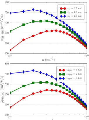
Fig. 2. Phonons + Metal grains limited electron mobility as a function of carrier density for different grain sizes (with average diameter D). The phonon-limited mobility is plotted for comparison. The thickness of the SiO2
and HfO2 layers is tox= 1 nm and tHfO2= 2 nm, respectively.
No attention has been paid to the impact of these fluctuations on the carrier mobility in long channels.
We focus here on Titanium Nitride (TiN), one of most technologically relevant metal gate materials. It is known to form grains with size in the 2 nm to 20 nm range. Depending on the grain orientation, the work function may vary between 4.6 eV (h100i orientation with 60% abundance) and 4.4 eV (h111i orientation with 40% abundance). The workfunction and gate potential may therefore vary by ∆WF = ±0.1 eV [3] from one grain to the other. An example of grain pattern (local workfunction fluctuations) is shown in Fig. 1. The average size of the grains is D = 5 nm. To generate such a pattern, we choose N = W L/(πD2) random seed points at
the metal/HfO2interface and define the grain associated with
each seed as the set of points closer to that seed than to any other. The workfunction of each grain is then either WF = 4.6 eV with 60% chance and 4.4 eV with 40% chance.
We first examine how the electron mobility depends on the grain size. The total phonons (PH) + metal grains (MG) mobility µPH+MG is plotted in Fig. 2. There is a significant
degradation of the mobility at low carrier densities. Metal grain scattering therefore behaves, in this respect, as RCS. The mobility gets worse with increasing grain size at least up to D = 10 nm.
In order to find an unique signature of MG scattering, we have analyzed how the phonon + MG mobility depends on the thickness of the SiO2 (tox) and HfO2 (tHfO2) layers and compared with the phonon + RCS mobility. The results are plotted in Fig. 3. We find that the phonon + MG mobility increases with increasing tox. This is also true for the phonon +
RCS mobility [13]: the disorder moves away from the channel in both cases. However, the phonon + MG mobility increases with increasing tHfO2, while the phonon + RCS mobility de-creases. [13]. Indeed, the effects of workfunction fluctuations are washed out when the gate is moved away from the channel,
Fig. 3. Phonons + Metal grains limited electron mobility as a function of carrier density, for different thickness of the SiO2layer tox(tHfO2 = 2 nm,
upper panel) and different thickness of the HfO2layer (tox= 1 nm, lower
panel). The average grain size is D = 5 nm.
while the effects of RCS charges at the SiO2/HfO2 interface
are enhanced because they are not screened as efficiently by the gate.
We can quantify these trends on the partial RCS and MG mobilities. They are defined from Matthiessen’s rule as µ−1M = µ−1PH+M− µ−1PH, where “M” is a given scattering mechanism (MG or RCS), and phonons (PH) are taken as a reference [5]. The dependence of the partial RCS and MG mobilities on tox
and tHfO2 are plotted in Fig. 4, at low carrier density n = 2 × 1012cm−2. The RCS mobility decreases almost exponentially with decreasing tox , and so does the MG mobility (Fig. 4).
Yet the the MG mobility increases with increasing tHfO2 (as the gate is moved away from the channel), while the RCS mobility decreases (as the RCS charges are less screened by the gate).
B. Scattering by interface dipoles
In addition to MG scattering, we have analyzed scattering by dipoles (instead of charges) at the SiO2/HfO2 interface. These
dipoles might result from the incorporation of metal dopants in HfO2to modulate the threshold voltage for example [14]. The
dipoles are perpendicular to the interface and are treated in the same way as RCS in the NEGF solver [5]. In the following,
Fig. 4. Partial RCS, MG and DP mobilities as a function of tox (tHfO2 =
2 nm, upper panel) and tHfO2 (tox = 1 nm, lower panel), at low carrier
density n = 2 × 1012cm−2. For MG, the average grain size is D = 5 nm, while the density of RCS (or DP) charges is n = 1013cm−2.
the density of interface dipoles is nDP= 1013 cm−2 and the
magnitude of each dipole is p = 0.5e · nm.
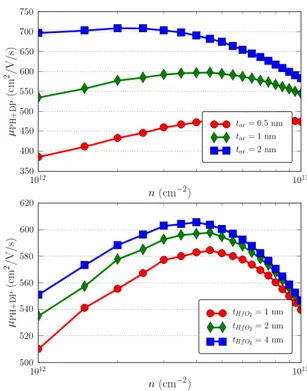
The computed phonons (PH) + interface dipoles (DP) mobility µPH+DP is plotted as a function of the inversion
density in Fig. 5. Similarly to the MG and RCS scattering, interface dipoles also cause a significant degradation of the mobility at low carrier densities [1]. The total PH + DP mobility increases with increasing either toxor tHfO2 (see Fig. 6) – though the mobility shows a much weaker dependence on tHfO2 than on tox. Namely, the partial DP mobility µDP increases exponentially with increasing tox, as for MG and
RCS scattering (see Fig. 4). In contrast with RCS however, it weakly increases with increasing tHfO2. Indeed, while the field created by a single charge at the SiO2/HfO2interface is better
screened when decreasing tHfO2 (because the image charge in the metal is opposite), the field created by a single dipole is enhanced (because the image dipole is the same sign). The partial DP mobility is expected to behave as 1/(nDP× p2).
Fig. 5. Phonons + interface dipoles (DP) limited electron mobility as a function of carrier density with tox = 1 nm and tHfO2 = 2 nm. The
density of local dipoles is nDP = 1013 cm−2 and the dipole strength is
p = 0.5e · nm. The phonon-limited mobility is plotted for comparison.
Fig. 6. Phonons + interface dipoles (DPs) limited electron mobility as a function of carrier density, for different thickness of the SiO2 layer tox
(tHfO2 = 2 nm, upper panel) and different thickness of the HfO2 layer
(tox= 1 nm, lower panel).
C. Discussion
The scattering by RCS charges, dipoles at the SiO2/HfO2
in-terface or metal gate workfunction fluctuations show different dependences on tHfO2. These mechanisms are not exclusive one from the other, so that the actual mobility in a device is certainly a combination of RCS, MG and DP contributions.
Yet a detailed analysis of the dependence of the mobility on toxand tHfO2might help to identify the dominant mechanism. Note that workfunction fluctuations have little impact on the threshold voltage as they average to ∼ 0. Both charges and dipoles at the SiO2/HfO2 interface result in significant
threshold voltage shifts unless they also average to zero (i.e., distribution of positively and negatively charged traps at the interface, or distribution of up and down dipoles). Fluctuations in the band alignment at the SiO2/HfO2 interface due to
non-homogeneities at this interface [15] could actually be mimicked by a distribution of dipoles at the interface with zero average.
IV. CONCLUSIONS
In the Non-equilibrium Green’s Functions framework, we have studied carrier scattering by metal grain (MG) work-function fluctuations and by dipoles (DP) at the SiO2/HfO2
interface in high-κ/metal gate stacks. Both workfunction fluc-tuations and interface dipoles result in a significant degradation of the mobility, especially at low carrier densities. In this respect, they behave the same as Remote Coulomb Scattering (RCS) by charges at the SiO2/HfO2 interface. However, the
RCS mobility decreases with increasing HfO2thickness, while
the MG mobility significantly increases and the DP mobility only weakly increases. These different dependences might provide a way to identify the dominant scattering mechanism experimentally.
ACKNOWLEDGEMENT
This work was supported by the French National Research Agency (ANR) project Noodles, and partly supported by the European Union Horizon 2020 research and innovation program under grant agreement No. 688101 SUPERAID7. The calculations were run on the TGCC/Curie machine thanks to allocations from GENCI and PRACE.
REFERENCES
[1] P. Toniutti, P. Palestri, D. Esseni, F. Driussi, M. De Michielis, and L. Selmi, “On the origin of the mobility reduction in n-and p-metaloxidesemiconductor field effect transistors with hafnium-based/metal gate stacks,” J. Appl. Phys., vol. 112, no. 3, p. 034502, 2012.
[2] V. H. Nguyen, Y. M. Niquet, F. Triozon, I. Duchemin, O. Nier, and D. Rideau, “Quantum Modeling of the Carrier Mobility in FDSOI Devices,” IEEE Transactions on Electron Devices, vol. 61, no. 9, pp. 3096–3102, 2014.
[3] H. F. Dadgour, K. Endo, V. K. De, and K. Banerjee, “Grain-Orientation Induced Work Function Variation in Nanoscale Metal-Gate Transistors– Part I: Modeling, Analysis, and Experimental Validation,” IEEE Trans. Electron Devices, vol. 57, no. 10, pp. 2504–2514, 2010.
[4] J. Wang, E. Polizzi, and M. Lundstrom, “A three-dimensional quan-tum simulation of silicon nanowire transistors with the effective-mass approximation,” J. Appl. Phys., vol. 96, no. 4, pp. 2192–2203, 2004. [5] Y.-M. Niquet, V.-H. Nguyen, F. Triozon, I. Duchemin, O. Nier, and
D. Rideau, “Quantum calculations of the carrier mobility: Methodology, Matthiessen’s rule, and comparison with semi-classical approaches,” J. Appl. Phys., vol. 115, no. 5, p. 054512, 2014.
[6] L. Bourdet, J. Li, J. Pelloux-Prayer, F. Triozon, M. Casse, S. Barraud, S. Martinie, D. Rideau, and Y.-M. Niquet, “Contact resistances in trigate and FinFET devices in a non-equilibrium Green’s functions approach,” J. Appl. Phys., vol. 119, no. 8, p. 084503, 2016.
[7] A. Yagishita, T. Saito, K. Nakajima, S. Inumiya, K. Matsuo, T. Shibata, Y. Tsunashima, K. Suguro, and T. Arikado, “Improvement of threshold voltage deviation in damascene metal gate transistors,” IEEE Transac-tions on Electron Devices, vol. 48, no. 8, pp. 1604–1611, 2001. [8] H. Dadgour, V. De, and K. Banerjee, “Statistical modeling of
metal-gate Work-Function Variability in emerging device technologies and implications for circuit design,” in Proc. of Int. Conf. on Computer Aided Design, 2008, pp. 270–277.
[9] A. R. Brown, J. R. Watling, and A. Asenov, “Intrinsic parameter fluctuations due to random grain orientations in high-κ gate stacks,” J. Comput. Electron., vol. 5, no. 4, pp. 333–336, 2006.
[10] S. Agarwal, R. K. Pandey, J. B. Johnson, A. Dixit, M. Bajaj, S. S. Furkay, P. J. Oldiges, and K. V. R. M. Murali, “Ab initio Study of Metal Grain Orientation-Dependent Work Function and its Impact on FinFET Variability,” IEEE Trans. Electron Devices, vol. 60, no. 9, pp. 2728–2733, 2013.
[11] S. M. Nawaz, S. Dutta, A. Chattopadhyay, and A. Mallik, “Comparison of Random Dopant and Gate-Metal Workfunction Variability Between Junctionless and Conventional FinFETs,” IEEE Electron Device Lett., vol. 35, no. 6, pp. 663–665, 2014.
[12] M. Bajaj, K. Nayak, S. Gundapaneni, and V. R. Rao, “Effect of Metal Gate Granularity Induced Random Fluctuations on Si Gate-All-Around Nanowire MOSFET 6-T SRAM Cell Stability,” IEEE Trans. Nanotechnol., vol. 15, no. 2, pp. 243–247, 2016.
[13] P. Toniutti, P. Palestri, D. Esseni, and L. Selmi, “Revised analysis of the mobility and ion degradation in high-κ gate stacks: Surface optical phonons vs. remote coulomb scattering,” in ESSDERC 2008 - 38th European Solid-State Device Research Conference, Sept 2008, pp. 246– 249.
[14] P. D. Kirsch, P. Sivasubramani, J. Huang, C. D. Young, M. A. Quevedo-Lopez, H. C. Wen, H. Alshareef, K. Choi, C. S. Park, K. Freeman, M. M. Hussain, G. Bersuker, H. R. Harris, P. Majhi, R. Choi, P. Lysaght, B. H. Lee, H.-H. Tseng, R. Jammy, T. S. Bscke, D. J. Lichtenwalner, J. S. Jur, and A. I. Kingon, “Dipole model explaining high-k/metal gate field effect transistor threshold voltage tuning,” Applied Physics Letters, vol. 92, no. 9, p. 092901, 2008.
[15] Y.-M. Niquet and C. Delerue, “Band offsets, wells, and barriers at nanoscale semiconductor heterojunctions,” Phys. Rev. B, vol. 84, p. 075478, Aug 2011.