HAL Id: cea-00308133
https://hal-cea.archives-ouvertes.fr/cea-00308133
Submitted on 20 Aug 2008
HAL is a multi-disciplinary open access
archive for the deposit and dissemination of
sci-entific research documents, whether they are
pub-lished or not. The documents may come from
teaching and research institutions in France or
abroad, or from public or private research centers.
L’archive ouverte pluridisciplinaire HAL, est
destinée au dépôt et à la diffusion de documents
scientifiques de niveau recherche, publiés ou non,
émanant des établissements d’enseignement et de
recherche français ou étrangers, des laboratoires
publics ou privés.
Growth of one-dimensional Si/SiGe heterostructures by
thermal CVD
Céline Mouchet, Laurence Latu-Romain, Cyril Cayron, Emmanuelle Rouvière,
Caroline Celle, Jean-Pierre Simonato
To cite this version:
Céline Mouchet, Laurence Latu-Romain, Cyril Cayron, Emmanuelle Rouvière, Caroline Celle, et al..
Growth of one-dimensional Si/SiGe heterostructures by thermal CVD. Nanotechnology, Institute of
Physics, 2008, 19 (335603), �10.1088/0957-4484/19/33/335603�. �cea-00308133�
Nanotechnology 19 (2008) 335603 (4pp) doi:10.1088/0957-4484/19/33/335603
Growth of one-dimensional Si/SiGe
heterostructures by thermal CVD
Celine Mouchet
1, Laurence Latu-Romain
1, Cyril Cayron
2,
Emmanuelle Rouviere
1, Caroline Celle
1and Jean-Pierre Simonato
11CEA, LITEN, DTNM, LCH, 38054 Grenoble, France
2CEA, LITEN, DTH, Grenoble Electron Microscopy @ Minatec, 38054 Grenoble, France
E-mail:jean-pierre.simonato@cea.fr
Received 5 March 2008, in final form 27 May 2008 Published 7 July 2008
Online atstacks.iop.org/Nano/19/335603
Abstract
The first results on a simple new process for the direct fabrication of one-dimensional
superlattices using common CVD chambers are presented. The experiments were carried out in a 200 mm industrial Centura reactor (Applied Materials).
Low dimensionality and superlattices allow a significant increase in the figure of merit of thermoelectrics by controlling the transport of phonons and electrons. The monocrystalline nanowires produced according to this process are both one-dimensional and present
heterostructures, with very thin layers (40 nm) of Si and SiGe. Concentrations up to 30 at.% Ge were obtained in the SiGe parts.
Complementary techniques including transmission electronic microscopy (TEM), selected area electron diffraction (SAED), energy dispersive x-ray spectroscopy (EDS), scanning transmission electron microscopy (STEM) in bright field and high angle annular dark field (HAADF STEM), and energy-filtered transmission electron microscopy (EF-TEM) were used to characterize the nanoheterostructures.
S Supplementary data are available fromstacks.iop.org/Nano/19/335603
(Some figures in this article are in colour only in the electronic version)
One-dimensional nanostructures are emerging as outstanding building blocks in nanoscience and nanotechnologies [1–6]. Semiconducting nanowires have the potential for various appli-cations that include optoelectronics, sensing, nanoelectronics, and thermoelectricity. Thermoelectric materials are of inter-est for many applications and in particular for capturing waste heat since they allow the conversion of heat into electricity. These materials are experiencing a surge in research activity aimed at increasing their performance [7]. The latter depends on the material’s thermoelectric figure of merit ZT, given by ZT= S2σ T/κ where S is the thermoelectric power (Seebeck coefficient),σ is the electrical conductivity, T is the tempera-ture, andκ is the thermal conductivity. In order to achieve a high figure of merit, several strategies can be envisaged. Re-duction of the dimensionality to form two- or one-dimensional materials and superlattice structures allows a significant in-crease in the ZT by controlling the transport of phonons and electrons [8–10].
Recently, very promising results were obtained with silicon nanowires, proving that even pure silicon can lead
to high performance thermoelectric materials [11, 12]. Previously, Yang et al achieved the synthesis of Si/SiGe superlattice nanowires [13]. To realize the synthesis of these semiconductor nanowires with longitudinal ordered heterostructures, a hybrid process with a pulsed laser ablation system coupled to a chemical vapor deposition chamber was developed. Thermal conductivity measurements showed effectively that the κ values of the Si/SiGe superlattice nanowires are much lower than those of pure Si ones with similar diameters [14].
Among available processes for the synthesis of silicon based nanowires [15], the VLS (vapor–liquid–solid) method is by far the most common route to fabricate Si, Ge, or SiGe nanowires [16–23]. It is remarkable to note that, to our knowledge, no growth of Si/SiGe has been previously reported with unmodified CVD chambers. Though there are a variety of methods for synthesizing one-dimensional nanostructures containing heterojunctions, such as for instance MBE (molecular beam epitaxy) [2, 24], a general method expendable in common CVD chambers
Nanotechnology 19 (2008) 335603 C Mouchet et al Si water Si growth SiGe growth SiH4 SiH4 + GeH4 SiH4 Au T>500°C Dewetting Incubation multistep synthesis
Scheme 1. Schematic illustration of the fabrication process of Si/SiGe nanowires.
has not yet been described. We report herein the growth of Si/SiGe superlattice nanostructures via the VLS method using simply SiH4 and GeH4 as gas precursors, and their characterization by transmission electronic microscopy (TEM), selected area electron diffraction (SAED), energy dispersive x-ray spectroscopy (EDS), scanning transmission electron microscopy (STEM) in bright field and high angle annular dark field (HAADF STEM), and energy-filtered transmission electron microscopy (EF-TEM). TEM and SAED characterizations were conducted with a conventional Jeol 2000FX, and STEM and EF-TEM images were realized with a Jeol 2010FEF, both microscopes operating at 200 kV.
The growth of the Si/SiGe nanowires was performed according to the VLS method developed for pure Si nanowires [16–23], and more particularly using growth conditions developed for pure silicon nanowires on this reactor [23]. A 10 nm gold thin film was deposited on a (111)-oriented silicon wafer by physical vapor deposition and dewetting was realized during 10 min at 550◦C under H2 atmosphere. This process allowed transformation of the gold thin film into an array of gold droplets used as catalysts for mediating the growth of nanowires [22]. The wafer was placed in a 200 mm Centura reactor (Applied Materials) at 10 Torr. A constant flow rate of hydrogen as diluent gas was maintained during the experiment (10 slm), and temperature was set at 550 or 700◦C. The key point of the synthesis was the ability to control the composition of the gas precursors in the gas phase. At the beginning, pure silane was introduced in the reactor to ensure formation of the liquid Au–Si alloy (eutectic temperature: 363◦C) and the commencement of silicon nanowire growth after the incubation delay.
Block-by-block growth of Si/SiGe was carried out under a constant flow of SiH4gas (100 sccm) by turning the GeH4 mixing valve on and off. Depending on the expected Ge concentration in SiGe, the germane flow was either 70 or 140 sccm. The successive feed-in of germane was done regularly so as to fabricate periodically changing slices of both Si and SiGe compositions (scheme1).
Figure 1 shows an STEM image of a nanowire grown at 700◦C with 70 sccm of germane and removed from the growth substrate by sonication (pure ethanol, 40 W, 30 s). The rather large diameter of the nanowire (∼450 nm) is inherent
Au
1 µm
Si SiGe
Figure 1. STEM image of a Si/SiGe nanowire superlattice grown at
700◦C. Dark areas are Ge enriched.
to the synthesis temperature, which is relatively high, and thus unfavorable to small diameters. The catalyst droplet remained at the tip of the nanowire and the basis was found to be larger than the mean diameter of the nanowire. The image reveals 18 light (Si) and 18 dark (SiGe) periodic layers, in agreement with the expected sequential composition of nanowires. EDS was used to evaluate the chemical composition of both regions. The ratio of x-ray signals corresponding to Si and Ge atoms gave an estimate of 14 at.% Ge in the SiGe phase. By a twofold increase of the germane flow (i.e. 140 sccm), the amount of Ge atoms in the crystalline structure was doubled, with an EDS measured content of 30 at.% Ge. This value is probably slightly underestimated due to the beam scattering in the nanowire. This indicates that by using this growth technique the Ge content can be fine tuned by regulating the germane flow during the synthesis of the nanowires.
In order to narrow down the diameters of the nanowires, further experiments were carried out at 550◦C. The germane flow was set to 140 sccm. Moreover, the gold film thickness was reduced to 2 nm instead of 10 nm to generate smaller gold droplets after dewetting. The nanowires obtained under these conditions were effectively narrower (diameter∼ 100±20 nm) and they also showed superlattices. The nanowire shown in figure 2 was fabricated under these conditions. It was composed of 45 periods of SiGe and 45 periods of Si layers. Smooth surfaces are obtained under these conditions whereas 2
500 nm
Figure 2. TEM image (bright field) of a Si/SiGe nanowire.
Figure 3. Result of using a 90/60 eV EF-TEM image ratio obtained
on the Si/SiGe superlattice nanowire. The SiGe layers appear in white. Inset: qualitative profile of Ge content along the nanowire axis between 0 and 30 at.%.
rather rough surfaces are revealed at higher temperature (figure1). Though this surface roughness is not well controlled and understood at this point, it may actually be of interest for the thermoelectric properties of these materials [12].
The layers with different compositions are only slightly visible, because the contrast is rather low due to low mass contrast between Si and SiGe parts, and because of the absence of diffraction contrast. In order to obtain a more accurate mapping of the Ge atoms in the nanowire, EF-TEM experiments were carried out according to a specific procedure [25] on nanowires containing∼30% Ge atoms in the SiGe layers. The contrast obtained using a two-window EF-TEM 90/60 eV ratio gives an accurate visualization of Ge distribution (figure3). Even though the superlattice appears clearly, some diffusion of Ge atoms into the Si parts of the nanowire is obvious. This might be simply due to the fact that germane was introduced sequentially into the reactor, without complete atmosphere purging. Thus, some Ge species probably remained in the gas phase when pure SiH4 was fed in during the CVD process. Nevertheless, the image shows unequivocally the alternation of Si and SiGe layers, with very thin slice thickness (around 50 nm).
Scanning transmission electron microscopy (HAADF STEM) was also performed for the chemical mapping of the nanowires (figure 4). The spot size was below 1 nm. Besides the longitudinal ordered heterostructure imaging, some tiny gold particles were observed along the nanowire surface. This was also observed on high magnification SEM images of pure Si nanowires, with sometimes new catalytic growth of very slender nanowires (figure S1 available at stacks.iop.org/Nano/19/335603). Despite some recent investigation on the surface migration of gold during the synthesis, this phenomenon remains unclear, and it is undoubtedly experimental conditions dependent [26–29]. However, for electronic or thermoelectric applications, gold can be easily removed from the nanowires by chemical gold removers [30].
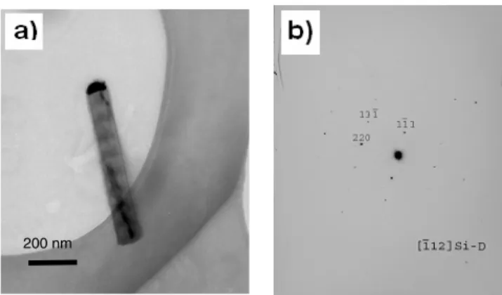
The crystalline nature of the nanowires was characterized on the nanowire shown in figure 5(a) by SAED (diffraction pattern, figure5(b)). This nanowire came from the same batch as those used for EF-TEM experiments (i.e. ∼30 at.% Ge content in SiGe parts). Analysis on a few nanowires showed that the growth occurs mainly along the [112] direction. The aperture used for the SAED experiments was approximately four times larger than the nanowire diameter, leading to the observation of many Si and SiGe layers. Diffractions show that the nanowires have a very good crystallinity, in agreement with Yang et al [12]. Moreover, no splitting of the diffraction
Nanotechnology 19 (2008) 335603 C Mouchet et al
200 nm
Figure 5. (a) Bright field image of a nanowire and (b) its SAED
diffraction pattern.
spots could be observed, even at high frequencies, which demonstrates the epitaxy between the Si and SiGe layers.
In summary, Si/SiGe superlattice nanowires were synthesized by simple modulation of the gas composition, and more specifically the germane content, during the growth. These nanomaterials were characterized by complementary electronic microscopy techniques. The fabrication process is simple and can be carried out in any common CVD chamber, as for example the 200 mm industrial reactor used in this study. We believe that this technique could be extended to detailed compositions and structures of one-dimensional superlattices and should give access to high performance materials for thermoelectric applications. Experiments are ongoing for adding dopants during the synthesis, which should improve the electrical conductivity and thus increase the thermoelectric figure of merit of these nanoheterostructures.
Acknowledgments
This research was supported by the European project Hydromel NMP2-CT-2006-026622. The authors would like to acknowledge Dr Natalio Mingo, Pascal Faucherand, and Severine Poncet for their help, and Dr Laure Guetaz and Dr Dominique Lafond for HAADF-STEM and EF-TEM experiments.
References
[1] Lu W and Lieber C M 2007 Nat. Mater.6 841–50
[2] Mieszawska A J, Jalilian R, Sumanasekera G U and Zamborini F P 2007 Small5 722–56
[3] Chen L J 2007 J. Mater. Chem.17 4639–43
[4] Lieber C M and Wang Z L 2007 MRS Bull. 32 99–108 [5] Patolsky F, Timko B P, Zheng G and Lieber C M 2007
MRS Bull. 32 142–9
[6] Sun Y and Rogers J A 2007 Adv. Mater.19 1897–916
[7] Snyder G F and Toberer E S 2008 Nat. Mater.7 105–14
[8] Venkatasubramanian R, Siivola E, Colpitts T and O’Quinn B 2001 Nature413 597–602
[9] Hicks L D and Dresselhaus M S 1993 Phys. Rev. B47 16631–4
[10] Yang C C, Armellin J and Li S 2008 J. Phys. Chem. C
112 1482–6
[11] Boukai A I, Bunimovich Y, Tahir-Kheli J, Yu J K,
Goddard W A III and Heath J R 2008 Nature451 168–71
[12] Hochbaum A I, Chen R, Delgado R D, Liang W, Garnett E C, Najarian M, Majumdar A and Yang P 2008
Nature451 163–8
[13] Wu Y, Fan R and Yang P 2002 Nano Lett.2 83–6
[14] Li D, Wu Y, Fan R, Yang P and Majundar A 2003
Appl. Phys. Lett.83 3186–8
[15] Teo B K and Sun X H 2007 Chem. Rev.107 1454–532
[16] Wagner R S and Ellis W C 1964 Appl. Phys. Lett.4 89–90
[17] Givargizov E I 1975 J. Cryst. Growth31 20–30
[18] Westwater J, Gosain D P, Tomiya S, Usui S and Ruda H 1997
J. Vac. Sci. Technol. B15 554–7
[19] Morales M and Lieber C M 1998 Science279 208–11
[20] Yu B, Sun X H, Calebotta G A, Dholakia G R and Meyyappan M J 2006 J. Cluster Sci.17 579–97
[21] Zhang X, Lew K K, Nimmatoori P, Redwing J M and Dickey E C 2007 Nano Lett.7 3241–5
[22] Sharma S, Kamins T I and Williams R S 2005 Appl. Phys. A
80 1225–30
[23] Latu-Romain L, Mouchet C, Cayron C, Rouviere M and Simonato J-P 2008 J. Nanopart. Res. 10 at press
[24] Zakharov N D, Werner P, Gerth G, Schubert L, Sokolov L and Gosele U J 2006 J. Cryst. Growth290 6–10
[25] Pantel R, Jullian S, Delille D, Dutartre D, Chantre A, Kermarrec O, Campidelli Y and Kwakman L F 2003
Micron34 239–47
[26] Hannon J B, Kodambaka S, Ross F M and Tromp R M 2006
Nature440 69–71
[27] Kodambaka S, Hannon J B, Tromp R M and Ross F M 2006
Nano Lett.6 1292–6
[28] G¨osele U 2006 Nature440 34–5
[29] Kawashima T, Mizutani T, Nakagawa T, Torii H, Saitoh T, Komori K and Fujii M 2008 Nano Lett.8 362–8
[30] Woodruff J H, Ratchford J B, Goldthorpe A, McIntyre P C and Chidsey C E D 2007 Nano Lett.7 1637–42