Broadband Transparent Optical Phase Change Materials
The MIT Faculty has made this article openly available.
Please share
how this access benefits you. Your story matters.
Citation
Zhang, Yifei, et al. "Broadband Transparent Optical Phase Change
Materials." Conference on Lasers and Electro-Optics, 14-19 May,
2017, San Jose, California, OSA, 2017, p. JTh5C.4. © 2017 Optical
Society of America
As Published
https://doi.org/10.1364/CLEO_AT.2017.JTh5C.4
Publisher
Optical Society of America
Version
Author's final manuscript
Citable link
http://hdl.handle.net/1721.1/114692
Terms of Use
Creative Commons Attribution-Noncommercial-Share Alike
This material is based upon work supported by the Assistant Secretary of Defense for Research and Engineering under Air Force Contract No. FA8721-05-C-0002 and/or FA8702-15-D-0001. Any opinions, findings, conclusions or recommendations expressed in this material are those
of the authors and do not necessarily reflect the views of the Assistant Secretary of Defense for Research and Engineering.
Broadband transparent optical phase change materials
Yifei Zhang1, Junying Li2, Jeffrey B. Chou3, Zhuoran Fang1, Anupama Yadav4, Hongtao Lin1, Qingyang Du1, JeromeMichon1, Zhaohong Han1, Yizhong Huang1, Hanyu Zheng1, Tian Gu1, Vladimir Liberman3, Kathleen Richardson4, Juejun Hu1,*
1Department of Materials Science and Engineering, Massachusetts Institute for Technology, Cambridge, MA, USA 2The Key Laboratory of Optoelectronic Technology & System, Education Ministry of China, Chongqing University, Chongqing, China
3Lincoln Laboratory, Massachusetts Institute of Technology Lexington, Massachusetts, USA 4College of Optics and Photonics, University of Central Florida, Orlando, Florida, USA
Abstract: We report a new group of optical phase change materials Ge-Sb-Se-Te (GSST) with low
loss from telecom bands to LWIR. We further demonstrated GSST-integrated SiN photonics with significantly improved switching performance over conventional GST alloys.
2017 Optical Society of America
OCIS codes: (160.3130) Integrated optics materials; (160.4670) Optical materials
Optical phase change materials (O-PCMs) are a unique class of materials which exhibit extraordinarily large optical property change (e.g. index change n > 1) when undergoing a solid-state phase transition. These materials, exemplified by Mott insulators such as VO2 and chalcogenide alloys (ChAs) such as Ge-Sb-Te (GST) compounds, have been exploited for a plethora of emerging optical applications including optical switching, photonic memories, reconfigurable metasurface, and non-volatile display [1-5]. These traditional phase change materials, however, generally suffer from large optical losses even in their dielectric states. For instance, the archetypal ChA phase change material GST is optically absorbing at the telecommunication bands due to its small bandgap and the resulting interband absorption, whereas its crystalline form is plagued by high free carrier absorption (FCA) in the mid-wave and long-wave infrared (LWIR) (Fig. 1a). The large optical losses fundamentally limit the performance of photonic devices based on traditional O-PCMs. We define the optical figure-of-merit (FOM) for O-PCMs as: FOM = n/k, where n is the index change upon phase transition and k denotes the extinction coefficient. It can be directly shown that this FOM dictates the attainable insertion loss and contrast ratio of tunable optical devices based on O-PCMs [6].
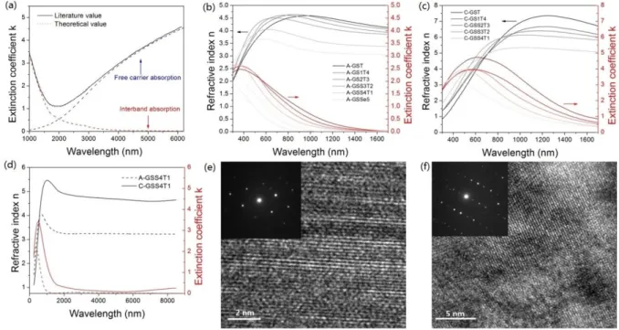
Figure 1: (a) Optical absorption of the classical phase change alloy Ge2Sb2Te5 fitted to show combined contributions from interband transition, Urbach tail, and FCA based on Drude models; (b, c) optical properties of GSST alloys in their (b) amorphous and (c) crystalline states; (d) optical properties of amorphous (dashed lines) and crystalline (solid lines) Ge2Sb2Se4Te1 from the visible range to LWIR; (e, f) TEM image and SAED patterns of crystallized (e) Ge2Sb2Se4Te1 and (f) Ge2Sb2Se5.
Here we report the synthesis, characterization and device integration of a new class of O-PCMs, Ge-Sb-Se-Te (GSST) alloys. A series of GSST thin films with the compositions of Ge2Sb2SexTe5-x (x = 1, 2, 3, 4, and 5) were prepared using thermal evaporation. We experimentally validated that Se substitution of Te results in an increase in optical band gap, enabling low loss operation in the technologically important 1310 nm and 1550 nm telecommunication bands (Figs. 1b and 1c). Meanwhile, the GSST materials claim reduced free carrier concentrations and mobility compared to GST as revealed by Hall measurements, which effectively suppresses FCA in the infrared. As an example, Fig. 1d shows that the Ge2Sb2Se4Te1 (GSS4T1) material features broadband transparency covering 1 micron to the LWIR. The large index contrast between the amorphous and crystalline states (n = 1.8) and the low optical loss of the GSS4T1 alloy lead to an exceptionally large FOM of > 900 at 1550 nm wavelength, over 20 times larger than that of the classical Ge2Sb2Te5 (GST 225) phase change alloy. Figures 1e and 1f present high-resolution TEM images and selected area electron diffraction (SAED) patterns (insets) of the GSS4T1 and Ge2Sb2Se5 alloys in their crystalline form. Unlike GST which exhibits an intermediate cubic phase during transition, GSS4T1 directly crystallizes into a hexagonal structure. On the other hand, the Ge2Sb2Se5 alloy forms an orthorhombic structure which is not reported in the classical GST group.
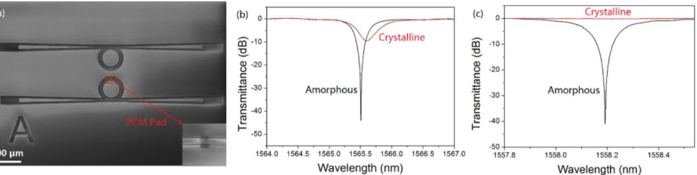
Figure 2: (a) SEM images of fabricated ring resonator devices; (b, c) transmission spectra of (b) GST-based device and (c) GSS4T1-based device.
To demonstrate the enhanced optical performance of the new O-PCMs, we deposited and patterned via lift-off GSST and GST patterns on single-mode SiN waveguide resonator devices fabricated following standard CMOS process protocols detailed elsewhere [7]. Figures 2b and 2c plot the transmittance spectra of SiN micro-ring devices integrated with the classical GST 225 phase change material and the GSS4T1 alloy when they are switched from amorphous to crystalline state. The device integrated with the GSS4T1 material claims a large on/off contrast ratio of 41 dB and an insertion loss of 0.2 dB, both of which represent significant improvements compared to state-of-the-art GST-based devices [1, 8]. Reversible switching of the GSS4T1 material using 4 ns laser pulses was also experimentally validated. Our theoretical model shows that improved cavity Q-factor due to reduced parasitic optical loss from GSST and enhanced switching contrast benefiting from the large FOM account for the performance boost.
In sum, we have demonstrated a new group of optical phase change materials Ge-Sb-Se-Te featuring broadband optical transparency covering the telecom bands up to LWIR. We anticipate that the materials will open up numerous emerging applications based on non-volatile photonic reconfiguration capitalizing on the enhanced optical performance of the materials compared to conventional phase change alloys.
References
1. M. Rudé, J. Pello, R. E. Simpson, J. Osmond, G. Roelkens, J. J. van der Tol, and V. Pruneri, "Optical switching at 1.55 μm in silicon racetrack resonators using phase change materials," Appl Phys Lett 103, 141119 (2013).
2. Q. Wang, E. T. F. Rogers, B. Gholipour, C. M. Wang, G. H. Yuan, J. H. Teng, and N. I. Zheludev, "Optically reconfigurable metasurfaces and photonic devices based on phase change materials," Nat Photonics 10, 60-65 (2016).
3. C. Ríos, M. Stegmaier, P. Hosseini, D. Wang, T. Scherer, C. D. Wright, H. Bhaskaran, and W. H. Pernice, "Integrated all-photonic non-volatile multi-level memory," Nat Photonics 9, 725-732 (2015).
4. P. Hosseini, C. D. Wright, and H. Bhaskaran, "An optoelectronic framework enabled by low-dimensional phase-change films," Nature 511, 206-211 (2014).
5. A.-K. U. Michel, D. N. Chigrin, T. W. Maß, K. Schönauer, M. Salinga, M. Wuttig, and T. Taubner, "Using low-loss phase-change materials for mid-infrared antenna resonance tuning," Nano Lett 13, 3470-3475 (2013).
6. X. Y. Sun, Q. Du, T. Goto, M. C. Onbasli, D. H. Kim, N. M. Aimon, J. Hu, and C. A. Ross, "Single-step deposition of cerium-substituted yttrium iron garnet for monolithic on-chip optical isolation," ACS Photonics 2, 856-863 (2015).
7. Q. Du, Y. Huang, O. Ogbuu, W. Zhang, J. Li, V. Singh, A. M. Agarwal, and J. Hu, "Gamma radiation effects in amorphous silicon and silicon nitride photonic devices," Opt Lett 42, 587-590 (2017).
8. M. Stegmaier, C. Ríos, H. Bhaskaran, C. D. Wright, and W. H. Pernice, "Nonvolatile All‐Optical 1× 2 Switch for Chipscale Photonic Networks," Adv Opt Mater 5, 1600346 (2017).