Publisher’s version / Version de l'éditeur:
Applied Physics Letters, 98, 6, 2011
READ THESE TERMS AND CONDITIONS CAREFULLY BEFORE USING THIS WEBSITE. https://nrc-publications.canada.ca/eng/copyright
Vous avez des questions? Nous pouvons vous aider. Pour communiquer directement avec un auteur, consultez la première page de la revue dans laquelle son article a été publié afin de trouver ses coordonnées. Si vous n’arrivez pas à les repérer, communiquez avec nous à [email protected].
Questions? Contact the NRC Publications Archive team at
[email protected]. If you wish to email the authors directly, please see the first page of the publication for their contact information.
NRC Publications Archive
Archives des publications du CNRC
This publication could be one of several versions: author’s original, accepted manuscript or the publisher’s version. / La version de cette publication peut être l’une des suivantes : la version prépublication de l’auteur, la version acceptée du manuscrit ou la version de l’éditeur.
For the publisher’s version, please access the DOI link below./ Pour consulter la version de l’éditeur, utilisez le lien DOI ci-dessous.
https://doi.org/10.1063/1.3548544
Access and use of this website and the material on it are subject to the Terms and Conditions set forth at
Carrier dynamics between delocalized and localized states in type-II
GaAsSb/GaAs quantum wells
Baranowski, M.; Syperek, M.; Kudrawiec, R.; Misiewicz, J.; Gupta, J.A.; Wu,
X.; Wang, R.
https://publications-cnrc.canada.ca/fra/droits
L’accès à ce site Web et l’utilisation de son contenu sont assujettis aux conditions présentées dans le site LISEZ CES CONDITIONS ATTENTIVEMENT AVANT D’UTILISER CE SITE WEB.
NRC Publications Record / Notice d'Archives des publications de CNRC:
https://nrc-publications.canada.ca/eng/view/object/?id=f0ddbfa3-3d3d-416c-8473-198c067e05b0 https://publications-cnrc.canada.ca/fra/voir/objet/?id=f0ddbfa3-3d3d-416c-8473-198c067e05b0Carrier dynamics between delocalized and localized states in type-II
GaAsSb/GaAs quantum wells
M. Baranowski,1,a兲M. Syperek,1R. Kudrawiec,1J. Misiewicz,1J. A. Gupta,2X. Wu,2and R. Wang2
1
Institute of Physics, Wroclaw University of Technology, Wybrzeze Wyspianskiego, 2750-370 Wroclaw, Poland
2
Institute for Microstructural Sciences, National Research Council of Canada, Ottawa K1A 0R6, Canada
共Received 15 November 2010; accepted 6 January 2011; published online 10 February 2011兲 The carrier dynamics in type-II GaAsSb/GaAs quantum well 共QW兲 is investigated by time-resolved photoluminescence at low temperature. A detailed analysis of the experimental data reveal a complex carrier relaxation scenario involving both delocalized and localized states. We show that the QW emission is controlled by the dynamics of the band bending effect, related to temporal changes in the spatial charge separation near the GaAsSb/GaAs heterointerface, whereas localized states play a significant role in the carrier relaxation/redistribution between QW states. © 2011
American Institute of Physics. 关doi:10.1063/1.3548544兴
GaAsSb/GaAs quantum well 共QW兲 structures have at-tracted considerable attention for their potential application in optoelectronic and electronic devices. This interest is mostly driven by the unique band structure properties of the GaAsSb QWs, which are controlled by the Sb concentration. One of the most important features is the possibility to tune the conduction lineup from type-I to type-II band alignment.1–6While the type-I structures found their applica-tion in light emitting devices, the unique properties of type-II GaAsSb/GaAs heterostructures can result in substantial im-provements in the performance of near infrared detectors and heterojunction bipolar transistors.7,8 Type-II GaAsSb/GaAs QWs9–11 have also been used in the development of laser diodes emitting at 1.3 m, which may provide an interesting alternative to GaAs-based telecommunications lasers based on highly strained InGaAs/GaAs QWs, dilute nitride QWs, or InAs quantum dots.
In spite of several reports addressing the optical proper-ties of type-II GaAsSb/GaAs QWs, there is still a lack of comprehensive studies on the carrier dynamics in this sys-tem. Previous experimental results in the literature3,4do not provide any detailed picture of the mechanisms for carrier relaxation. The main goal of this letter is to use time-resolved photoluminescence 共TRPL兲 to which may finally bring some understanding into the carrier relaxation pro-cesses in the type-II GaAsSb/GaAs quantum wells. We show a strong influence of the dynamic band bending effect4,12,13 on the observed PL kinetics and point out the important role of carrier trapping by localized states, which affects the re-laxation dynamics in the structure. Eventually, we propose a carrier relaxation scenario where the carrier transfer between delocalized and localized states plays an important role.
The investigated structure was grown on an N + GaAs共100兲 substrate in a molecular beam epitaxy system. The growth began with a 100 nm undoped GaAs buffer layer and 20-period 共2 nm GaAs/2 nm AlAs兲 superlattice followed by 200 nm of GaAs. The active region of the structure con-sists of two 7 nm GaAs0.8Sb0.2 wells separated by a 20 nm
GaAs barrier. It forms a double quantum well system with
holes and electrons confined in the GaAsSb and GaAs layer, respectively. The quantum coupling between the two QWs can be neglected because of very thick GaAs barrier. The active region was covered with a 100 nm GaAs layer and finally overgrown by a 50 nm layers of Al0.33Ga0.67As and
GaAs.
In the TRPL experiment, the sample was excited non-resonantly 共Elaser= 1.57 eV兲 by a mode-locked Ti:sapphire
laser with 3.8 MHz repetition rate and pulse duration of 160 fs. The PL signal was dispersed by a 0.3 m focal length spectrometer and detected by the S1 streak camera. The overall time resolution of the system was ⬃90 ps. In the case of continuous wave 共cw兲 experiments, the sample was excited at 532 nm 共2.33 eV兲 using a frequency-doubled neodymium-doped yttrium aluminium garnet; Nd:Y3Al5O12
共YAG兲 laser and the PL signal was detected by an InGaAs linear array detector.
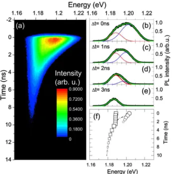
Figure 1共a兲 shows the TRPL emission from the active region of the investigated structure in the form of a streak image. The streak represents the time evolution of the PL emission intensity versus energy of the emitted photons. Its detailed analysis can give more insight into the observed PL signal. At first, we have extracted several horizontal intensity profiles taken at specific time intervals 共⌬t兲 after the excita-tion pulse arrival 关see Figs. 1共b兲–1共e兲兴. At ⌬t ⬇ 0, the PL band profile is asymmetric, suggesting a contribution of sev-eral optical transitions in the emission spectrum. We have concluded that the emission band can be well fitted using a sum of two Gauss functions, as shown in Figs. 1共b兲–1共d兲. Hence, we have shown that at least two optical transitions, the high and low energy ones, have a major impact on the observed PL emission from the active region of the investi-gated structure at an early time scale. Further analysis per-formed on the PL intensity profiles reveals that the position of the high energy transition shifts ⬃6 meV toward lower energy as the time elapses 关see circles in Fig.1共f兲兴. Simulta-neously, its intensity decreases monotonically and finally vanishes completely above ⌬t ⬃ 2.5 ns. The low energy op-tical transition behaves differently. There is no significant shift of its energy position up to ⌬t ⬃ 2.5 ns 关see squares in Fig.1共f兲兴. However, after crossing that point, its energy po-a兲
Electronic mail: [email protected].
APPLIED PHYSICS LETTERS 98, 061910 共2011兲
0003-6951/2011/98共6兲/061910/3/$30.00 98, 061910-1 © 2011 American Institute of Physics Downloaded 16 Feb 2011 to 132.246.27.224. Redistribution subject to AIP license or copyright; see http://apl.aip.org/about/rights_and_permissions
sition shifts to the red by ⬃10 meV on the several nanosec-onds time scale, which is accompanied by the intensity drop. Tentatively, we assigned the high energy PL emission to the optical transition involving the QW ground state, whereas the low energy PL emission is assigned to the radiative re-combination from the broad distribution of localized states 共LS兲. Next we will strengthen our conclusions by simple theoretical considerations and additional experimental evi-dence.
During energy relaxation processes, photoexcited carri-ers in a type-II system tend to spatial separation forced by the different electron and hole confinement regimes. Elec-trons captured by the conduction band potential minimum in the GaAs layer and holes trapped by the valence band poten-tial in the GaAsSb layer form an electric dipole. The band bending conditions are modified substantially by spatial charge separation close to the GaAsSb/GaAs heterointerface and thus can affect the energy of quantized levels in a dy-namic manner. The electric field 共兲 thus produced is propor-tional to number of carriers n injected to the active region and forms a triangularlike quantum well.12,13 The ground state energy 共E兲 in such a well depends on electric field as
E共t兲⬀ 共t兲2/3. 共1兲
Since 共t兲 is determined by the initial photoexcitation and by further recombination processes 关I共t兲 ⬃ dn / dt兴, Eq. 共1兲 sug-gests that the energy of quantized levels inside the QW will vary with I共t兲2/3 in a linear manner. This trend is clearly visible in Fig.2共circles兲 for the high energy transition. If the low energy transition originated from the QW, one would expect a similar linear shift of the transition energy. How-ever, the LS peak position depicted as squares in Fig. 2 be-haves differently. It remains constant up to the point when the QW is fully depleted 共⌬t ⬃ 2.5 ns兲 and is then redshifted,
followed by a substantial drop in intensity. The energy shift and intensity changes of this peak can be explained if we assume with the presence of localized states distributed be-low the QW ground state 共i.e., the mobility edge兲 and char-acterized by different trapping potential depth. The PL emis-sion from such states will be weakly affected by the electric field changes due to the strong electron 共hole兲 spatial con-finement. The observed shift of the peak position at ⌬t ⬎ 2.5 ns can be rather related to the carrier redistribution within the broad ensemble of localized states.14,15The local-ized states in the investigated structure are attributed to GaAsSb alloy inhomogeneities and QW interface roughness. To evaluate the contribution of the LS emission in the ob-served PL kinetics, we performed a standard CW experiment measuring the PL peak position versus temperature at low excitation conditions. Figure 3 shows that in the low tem-perature region, a strong deviation of the emission energy versus temperature is observed in relation to the theoretical expectations predicted by the Varshni formula. Such behav-ior is often attributed to carrier localization where the energy of recombining electron-hole pairs at low temperature is lowered by the binding energy of the trapping potential. However, at high temperatures, the thermal energy is suffi-ciently high to free the carriers from their traps. The local-ization energy in our case is of ⬃12 meV, which stays roughly similar to the ⬃10 meV given by the analysis of the streak image horizontal profiles in Fig.1and the energy shift dependence versus carrier density in Fig.2. We would like to note that CW PL spectra do not clearly reveal the double-peak feature due to averaging of the CW PL intensity over time. Nevertheless, if we look at the temperature dependence
FIG. 1. 共Color online兲 共a兲 Streak image of the PL emission for the active region of the investigated structure at 10 K 共Pexc= 0.4 W cm−2兲. 共b兲
Horizontal profiles of the streak image taken shortly after pulse arrival 共⌬t ⬇ 0 ps兲 and at a longer time scale together with their spectral compo-nents 关共c兲–共e兲兴. 共f兲 The peak position of the high energy 共circles兲 and low energy 共squares兲 spectral components together with their intensities indi-cated by the symbol size.
FIG. 2. 共Color online兲 Dependence of the QW 共circles兲 and LS 共squares兲 emission peaks vs I2/3. The size of the points represents peak intensity.
FIG. 3. 共Color online兲 Temperature dependence of the CW PL peak energy position for the active region of investigated structure 共circles兲. The solid line represents a theoretical curve according to the Varshni equation. The inset shows the FWHM parameter vs temperature.
061910-2 Baranowski et al. Appl. Phys. Lett. 98, 061910 共2011兲
of the full width at half maximum 共FWHM兲 parameter 共inset in Fig.3兲, we can observe its nonmonotonic behavior, which indicates coexistence of two type transitions 共LC and QW emission兲 in the range of 40–80 K.
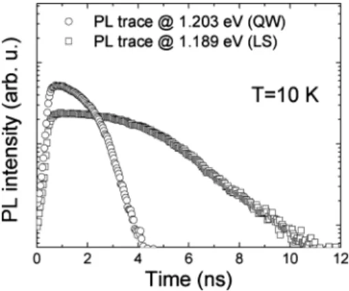
Let us now turn to the PL decay profiles. The first indi-cation of a multistage relaxation process in the active region of the structure is given in Fig. 1. It is well visible that the intensity of the QW transition indicated by the size of circles decreases monotonically up to ⌬t ⬃ 2.5 ns. However, over the same time scale, the LS peak intensity illustrated by the size of the squares in Fig. 1共f兲 remains nearly constant and starts to decrease at ⌬t ⬎ 2.5 ns. This suggests a state filling effect similar to that observed for quantum dots in high power optical pumping regimes.16This is further confirmed by the PL decay profiles demonstrated in Fig. 4, which shows two TRPL traces taken at the low energy side 共mostly contributed by the LS emission兲 and at the maximum of the total emission band 共dominated by the QW emission兲. With these excitation conditions, the high energy PL shows non-exponential decay preceded by a rather fast rise time. After an initial fast PL rise time, the low energy PL emission hibits an extensive plateau during the first ⬃2.5 ns after ex-citation and an acceleration of the PL decay after the point where the high energy emission drops by several orders of magnitude. This can be explained as follows. Just after exci-tation, carriers are trapped by their potential minima in the GaAs 共electrons兲 and GaAsSb layers 共holes兲, as indicated by the relatively fast PL rise time. However, a part of the pho-toexcitated carrier population is also efficiently trapped and distributed within the LS ensemble situated energetically be-low the QW mobility edge. The extended plateau observed for the LS emission is related with the population of the localized states from some higher lying states. The state fill-ing of LS is either provided by the direct relaxation from the barrier or by charge transfer from the QW. It appears that the
former relaxation channel can play a major role. This would be explained by the considerable speed up of the PL decay rate for the low energy transitions after complete depletion of the QW.
In conclusion, we have investigated the PL kinetics from GaAsSb QWs with type-II conduction band alignment. De-tailed analysis of the PL intensity profiles at different times shows that the total PL emission band at the early stage after optical pulse excitation is dominated by the emission from the delocalized and localized states. We have shown that the observed PL kinetics are strongly influenced by the dynamic of band bending conditions resulting from the dynamic change of the spatial charge separation near the GaAsSb/ GaAs heterointerface. Analysis of the PL decay profiles at different emission energy confirmed a multistage relaxation process in the active region of the investigated structure. We point out the important role of the charge transfer between delocalized and localized states.
M.S. acknowledges financial support from the Founda-tion of Polish Science within the START program. Part of the research was realized within the NLTK Project No. POIG.02.02.00-00-003/08-00.
1
G. Liu, S.-L. Chuang, and S.-H. Park,J. Appl. Phys. 88, 5554 共2000兲.
2
R. Teissier, D. Sicault, J. C. Harmand, G. Ungaro, G. L. Roux, and L. Largeau,J. Appl. Phys. 89, 5473 共2001兲.
3
M. Dinu, J. E. Cunningham, F. Quochi, and J. Shah,J. Appl. Phys. 94,
1506 共2003兲.
4
X. D. Luo, C. Y. Hu, Z. Y. Xu, H. L. Luo, Y. Q. Wang, J. N. Wang, and W. K. Ge,Appl. Phys. Lett. 81, 3795 共2002兲.
5
G. Ji, S. Agarwala, D. Huang, J. Chyi, and H. Morko,Phys. Rev. B 38,
10571 共1988兲.
6
J.-B. Wang, S. R. Johnson, S. A. Chaparro, D. Ding, Y. Cao, Yu. G. Sadofyev, Y.-H. Zhang, J. A. Gupta, and C. Z. Guo, Phys. Rev. B 70,
195339 共2004兲.
7
P.-J. Niu, H. H. H.-W. Dong, W. Wang, and J. Zhou,Proc. SPIE5624, 630
共2005兲.
8
X. Sun, S. Wang, X. G. Zheng, X. Li, J. C. Campbell, and A. L. Holmes, Jr.,J. Appl. Phys. 93, 774 共2003兲.
9
M. Yamada, T. Anan, K. Kurihara, K. Nishi, K. Tokutome, A. Kamei, and S. Sugou,Electron. Lett. 36, 637 共2000兲.
10
T. Anan, M. Yamada, K. Nishi, K. Kurihara, K. Tokutome, A. Kamei, and S. Sugou,Electron. Lett. 37, 566 共2001兲.
11
F. Quochi, J. Cunningham, M. Dinu, and J. Shah,Electron. Lett. 36, 2075
共2000兲.
12
N. N. Ledentsov, J. Böhrer, M. Beer, F. Heinrichsdorff, M. Grundmann, D. Bimberg, S. V. Ivanov, B. Y. Meltser, S. V. Shaposhnikov, I. N. Yass-ievich, N. N. Faleev, P. S. Kop’ev, and Zh. I. Alferov,Phys. Rev. B 52,
14058 共1995兲.
13
Y. S. Chiu, M. H. Ya, W. S. Su, and Y. F. Chen,J. Appl. Phys. 92, 5810
共2002兲.
14
T. S. Ko, T. C. Lu, T. C. Wang, J. R. Chen, R. C. Gao, M. H. Lo, H. C. Kuo, S. C. Wang, and J. L. Shen,J. Appl. Phys. 104, 093106 共2008兲.
15
T. Akasaka, H. Gotoh, Y. Kobayashi, H. Nakano, and T. Makimoto,Appl. Phys. Lett. 89, 101110 共2006兲.
16
S. Grosse, J. H. H. Sandmann, G. von Plessen, J. Feldmann, H. Lipsanen, M. Sopanen, J. Tulkki, and J. Ahopelto,Phys. Rev. B 55, 4473 共1997兲.
FIG. 4. The TRPL traces taken from the streak image in Fig.1. The high energy PL trace 共circles兲 is mostly due to the QW emission, whereas the low energy PL trace 共squares兲 is due to the LS emission.
061910-3 Baranowski et al. Appl. Phys. Lett. 98, 061910 共2011兲