Publisher’s version / Version de l'éditeur:
Journal Of Physics, 210, 2010-03-02
READ THESE TERMS AND CONDITIONS CAREFULLY BEFORE USING THIS WEBSITE. https://nrc-publications.canada.ca/eng/copyright
Vous avez des questions? Nous pouvons vous aider. Pour communiquer directement avec un auteur, consultez la
première page de la revue dans laquelle son article a été publié afin de trouver ses coordonnées. Si vous n’arrivez pas à les repérer, communiquez avec nous à [email protected].
Questions? Contact the NRC Publications Archive team at
[email protected]. If you wish to email the authors directly, please see the first page of the publication for their contact information.
Archives des publications du CNRC
This publication could be one of several versions: author’s original, accepted manuscript or the publisher’s version. / La version de cette publication peut être l’une des suivantes : la version prépublication de l’auteur, la version acceptée du manuscrit ou la version de l’éditeur.
For the publisher’s version, please access the DOI link below./ Pour consulter la version de l’éditeur, utilisez le lien DOI ci-dessous.
https://doi.org/10.1088/1742-6596/210/1/012019
Access and use of this website and the material on it are subject to the Terms and Conditions set forth at
Biexciton binding energy control in site-selected quantum dots
Reimer, M. E.; Dalacu, D.; Poole, P. J.; Williams, R. L.
https://publications-cnrc.canada.ca/fra/droits
L’accès à ce site Web et l’utilisation de son contenu sont assujettis aux conditions présentées dans le site LISEZ CES CONDITIONS ATTENTIVEMENT AVANT D’UTILISER CE SITE WEB.
NRC Publications Record / Notice d'Archives des publications de CNRC: https://nrc-publications.canada.ca/eng/view/object/?id=6ecb81d6-9257-4fa9-9674-c3d02aa22de2 https://publications-cnrc.canada.ca/fra/voir/objet/?id=6ecb81d6-9257-4fa9-9674-c3d02aa22de2
Biexciton binding energy control in site-selected
quantum dots
M. E. Reimer,1,2 D. Dalacu,1 P. J. Poole,1 and R. L. Williams1
1 Institute for Microstructural Sciences, National Research Council of Canada, Ottawa K1A 0R6, Canada
2 Kavli Institute of Nanoscience, Delft University of Technology, P.O. Box 5046, 2600 GA Delft, The Netherlands
E-mail: [email protected]
Abstract. A unique nanotemplate deposition technique is utilized in growth of semiconductor quantum dots which enables precise control over the dot dimensions and nucleation site. Here, we demonstrate tuning of the biexciton binding energy in a single, site-selected InAs/InP quantum dot through manipulation of the nanotemplate dimensions and thus, dot size. A monotonic decrease of the biexciton binding energy from the binding to anti-binding regime through zero is observed with increasing dot size. Piezoelectric fields in large quantum dots are suggested as the mechanism to obtain an unbound biexciton state. The tunability of the biexciton binding energy demonstrated here for a deterministically positioned quantum dot is an important step towards a scalable route in the generation of entangled photon pairs that emit around the telecommunications band of 1.55 µm.
1. Introduction
The generation of entangled photon pairs in semiconductor quantum dots relies heavily on the removal of the fine-structure splitting (FSS) of the intermediate exciton states in the biexciton-exciton radiative cascade [1]. Recent proposals to circumvent this requirement and thus produce entangled photon pairs even in the presence of non-zero FSS include the following: tuning of the biexciton binding energy to zero with a lateral electric field and time-reordering [2–5]; modulation of the exciton and biexciton energy levels with a frequency corresponding to the FSS [6]; and, coupling of the biexciton and exciton transitions to cavity modes with orthogonal polarizations [7]. Until now, experimental investigations of biexciton binding energy, ∆XX,
on dot size have been performed on randomly located quantum dots [8–13]. However, in this work, we demonstrate tuning of the biexciton binding energy by controlling the nanotemplate dimensions and thus, dot size of a single, site-selected InAs/InP quantum dot. In particular, the nanotemplate dimensions control the lateral dot dimensions, while the amount of dot material deposited controls the dot height and therefore exciton emission energy [14, 15]. Additionally, these results also investigate a new regime for the dependence of ∆XX on dot size in larger
quantum dots that emit near the telecommunications band of 1.55 µm, a wavelength range of interest for applications in quantum cryptography. Of particular importance is that ∆XX is
found to be directly influenced by the dimensions of the ridge nanotemplate. Here, ∆XX can be
tuned from the binding (bound) to antibinding (unbound) regime through zero – a regime not previously studied in large dots.
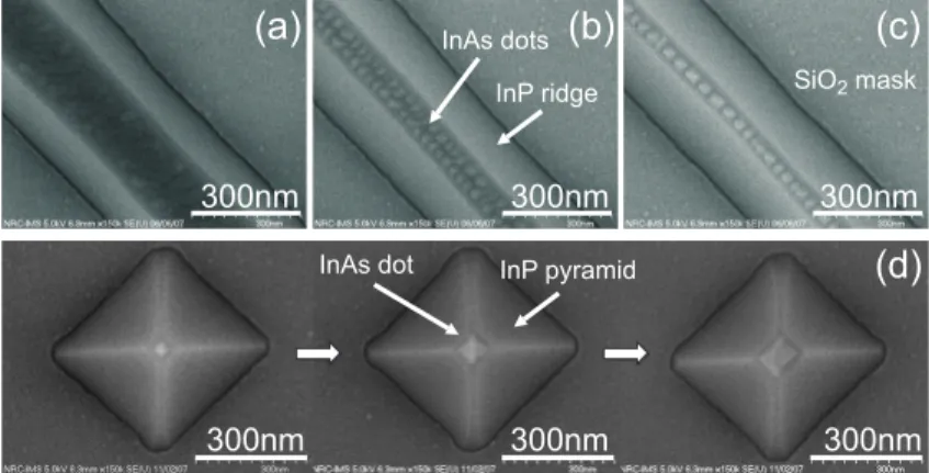
300nm InP ridge InAs dots (b) 300nm SiO mask2 (c) 300nm (a) 300nm 300nm 300nm (d) InP pyramid InAs dot
Figure 1. Plan view SEM images of uncapped ridge nanotemplates with varying base width dimensions: (a) 390 nm, (b) 335 nm, and (c) 325 nm. The top (001) surface lateral dimensions reduces with decreasing ridge base width until only a single row of quantum dots is obtained in (c). (d) Control of single dot dimensions via square-based nanotemplate. The base width dimensions of the nanotemplate increase from left to right, corresponding to an increase in dot size.
2. Sample
SEM images of ridge nanotemplate structures of ‘stripe’ geometry with varying base widths, w0,
produced under identical growth conditions are shown in Figure 1. Since the ridge nanotemplates are subject to identical growth conditions, larger starting base widths will result in a wider area available for quantum dot growth. If the ridge is sufficiently wide, dots are randomly distributed on top of the ridge in a manner similar to that of conventionally grown dots on planar substrates, as shown in Figure 1(a). As the top (001) surface, w, of the nanotemplate narrows, the dot growth is affected in two ways. First, the top width of the nanotemplate confines the area available for growth. When lateral dimensions are significantly reduced, the quantum dots will order on the top apex as to minimize the strain. The randomly distributed flat dots as shown in Figure 1(a) will transition to a double ordered dot array as shown in Figure 1(b). By reducing the ridge base width further, the lateral dimensions of the ridge (001) apex can only support a single row of quantum dots as shown in Figure 1(c). The lateral dimensions of the dots shown in Figure 1(c) are approximately 30-40 nm. Second, the amount of dot material (InAs) deposited on the top (001) surface is enhanced as the ratio of w0/w increases. This corresponds to an increase
in the quantum dot height and dot emission shift towards the telecommunications wavelength of 1.55 µm [15]. The increase in quantum dot height can be inferred by the enhanced contrast of the SEM images from Figures 1(a)-(c). To facilitate single dot isolation and application of lateral electric fields for entangled photon pair generation, a pair of Schottky gates with narrow 300 nm gaps are fabricated [2, 3, 16]. Similar control of the dot dimensions can be achieved on the single dot level as shown in Figure 1(d). Here, the template geometry is modified to a square-based nanotemplate.
3. Identification of exciton and biexciton in experiment
To identify the exciton (X) and biexciton (XX) in experiment, a combination of both power (state-filling spectroscopy) and polarization dependent spectroscopy of the observed photoluminescence (PL) emission spectra was conducted, similarly to previous studies [8,11,12]. Moreover, electric field dependence can be used as an additional experimental tool to identify the exciton and biexciton since Coulomb interactions play an important role [3,4]. Consequently, the exciton and biexciton exhibit unique signatures (i.e. Stark shifts, fine-structure, life time,
(a) Bound XX (b) Unbound XX
Figure 2. Typical state-shell filling spec-troscopy of (a) bound and (b) unbound biexciton for a single prepositioned quan-tum dot on ridge nanotemplate at zero elec-tric field. In the lower panel are fits (solid lines) to the data within the random cap-ture model. Evidence of exciton and biex-citon are inferred from the resulting linear and superlinear power dependence of inte-grated intensity on excitation power.
etc.) as a function of lateral electric field which allows the biexciton-exciton cascade to be differentiated from all other cascades, including charged excitonic states [3, 4].
Typical single dot PL for single, site-selected InAs/InP quantum dots as a function of increasing excitation power at zero electric field is shown in the upper panel of Figure 2. In Figure 2(a) the observed biexciton peak is bound, while in Figure 2(b) the biexciton is unbound. These assignments of X and XX transitions are determined within the random capture model by fitting the integrated intensity of the emission peaks as a function of excitation power [12]. Within this simple model, the slope is proportional to one and two for X and XX, respectively, which allows the observed optical transitions (X and XX) to be readily determined [12]. Excellent fits are obtained for both the bound and unbound biexciton cases, as shown in the lower panel of Figure 2. In addition, the saturation of both X and XX observed in experiment is well described by Poissonnian statistics for increasing excitation power. The assignment of X, and XX observed in experiment is confirmed in independent studies by polarization dependent spectroscopy and their electric field dependence [2, 3].
Consistent with literature, ∆XX = EX− EXX [8,11,12]. Here, a bound (unbound) biexciton
has a positive (negative) ∆XX and is found at lower (higher) energy than X. The biexciton
binding energy is a direct result of Coulomb interactions of the two electron-hole pairs building the biexciton and correlations of higher lying states [4]. The positive contributions to ∆XXarises
from e-h Coulomb attraction and correlation effects, while the negative component comes from the Coulomb repulsion between carriers of the same type. Thus, an unbound biexciton can be manifested in small dots from a weaker dependence on electron-hole Coulomb interactions than electron-electron and hole-hole Coulomb repulsion or when the number of bound states decreases, thus leading to a reduction in correlations [11]. In contrast, strain induced piezoelectric fields in large dots can result in a separation of charges, thus leading to an unbound biexciton state [9,13].
4. Biexciton binding energy tuning via ridge nanotemplate
The dependence of ∆XX on dot size for 19 individual InAs/InP quantum dots in ridge
nanotemplates is shown in Figure 3. In the data range for X emission similar to Chauvin et al. [13], the dependence of ∆XX on X emission energy is remarkably similar (bound XX regime). In addition, however, there is a transition from the bound to unbound XX regime
for decreasing X emission energy. The tuning range controlled via the ridge nanotemplate is rather large; ∆XX = +3.1 meV at X emission energy of 1011 meV, while ∆XX ≃ −4 meV near the telecommunications wavelength of 1.55 µm (800 meV). This corresponds to a controlled tuning range for ∆XX of 7.1 meV. The observed crossover point for zero XX binding energy (i.e.
∆XX = 0) occurs in the energy range between ∼ 910 − 930 meV. The resulting dependence of
∆XX on dot size is attributed to increases in piezoelectric fields with increasing dot size [9, 13].
Piezoelectric fields tend to separate charges which lead to an unbound XX state [9]; however, the antibinding regime has not been achieved yet in large quantum dots until this work. The antibinding regime for XX in large dots may be a very important step towards the realization of a scalable route for the generation of entangled photon pairs. The piezoelectric fields that produce a separation of charges leading to an antibinding XX state may also reduce the fine-structure splitting near zero since this splitting depends strongly on the electron-hole wavefunction overlap [3, 17]. Indeed, in the work of Chauvin et al., no FSS was observed within the spectral resolution of 100 µeV for large dots [13]. Similar results were obtained for the dots exhibiting an unbound XX state studied here within the spectral resolution of 50 µeV (data not shown).
Figure 3. Controlled tunability of biexciton binding energy, ∆XX, on dot size for ridge nanotemplate. Decreasing the
ridge base width increases the dot height for the same amount of dot material deposited and shifts the the excition emission energy towards the telecommunications band around 1.55 µm (800 meV), while reducing ∆XX. The scatter of ∆XX for
a given exciton emission energy is due to variations in the lateral dot dimensions for a given quantum dot height.
5. Summary
The controlled tunability of ∆XX via the ridge nanotemplate presented here for individual
InAs/InP quantum dots is desirable for the realization of a scalable route to producing entangled photon pair sources. With appropriate choice of the growth conditions, ∆XX can be engineered
to zero. In cases where there are small deviations from ∆XX = 0, a lateral electric field can be
used to remove the biexciton binding energy [2, 3].
Acknowledgments
The authors would like to acknowledge the financial support of the Natural Sciences and Engineering Research Council, QuantumWorks and the Business Development Bank of Canada.
References
[1] Stevenson R M, Young R J, Atkinson P, Cooper K, Ritchie D A and Shields A J 2006 Nature 439 179–182 [2] Reimer M E et al. 2007 Voltage induced hidden symmetry and photon entanglement generation in a single,
site-selected quantum dot (Preprint arXiv:0706.1075)
[3] Reimer M E, Korkusi´nski M, Dalacu D, Lefebvre J, Lapointe J, Poole P J, Aers G C, McKinnon W R, Hawrylak P and Williams R L 2008 Phys. Rev. B 78 195301
[4] Korkusinski M, Reimer M E, Williams R L and Hawrylak P 2009 Phys. Rev. B 79 035309
[5] Avron J E, Bisker G, Gershoni D, Lindner N H, Meirom E A and Warburton R J 2008 Phys. Rev. Lett. 100 120501
[6] Coish W A and Gambetta J M 2009 Sideband eraser of ‘which-path’ information for entangled photons on demand (Preprint arXiv/0907.0437)
[7] Pathak P K and Hughes S 2009 Phys. Rev. B 79 205416
[8] Rodt S, Heitz R, Schliwa A, Sellin R L, Guffarth F and Bimberg D 2003 Phys. Rev. B 68 035331 [9] Rodt S, Schliwa A, P¨otschke K, Guffarth F and Bimberg D 2005 Phys. Rev. B 71 155325
[10] Seguin R, Schliwa A, Rodt S, P¨otschke K, Pohl U W and Bimberg D 2005 Phys. Rev. Lett. 95 257402 [11] Sarkar D, van der Meulen H P, Calleja J M, Becker J M, Haug R J and Pierz K 2006 Journal of Applied
Physics 100023109
[12] Savio C D, Pierz K, Ade G, Danzebrink H U, G¨obel E and Hangleiter A 2006 Applied Physics B: Lasers and
Optics 84317–322
[13] Chauvin N, Salem B, Bremond G, Guillot G, Bru-Chevallier C and Gendry M 2006 Journal of Applied
Physics 100073702
[14] Lefebvre J, Poole P J, Fraser J, Aers G C, Chithrani D and Williams R L 2002 J. Cyrstal Growth 234 391–398
[15] Lefebvre J, Poole P J, Aers G C, Chithrani D and Williams R L 2002 J. Vac. Sci. Technol. B 20 2173–2176 [16] Reimer M E et al. 2008 Physica E: Low-dimensional Systems and Nanostructures 40 1790–1793