HAL Id: tel-01808972
https://hal.archives-ouvertes.fr/tel-01808972v2
Submitted on 1 Feb 2019
HAL is a multi-disciplinary open access archive for the deposit and dissemination of sci-entific research documents, whether they are pub-lished or not. The documents may come from teaching and research institutions in France or abroad, or from public or private research centers.
L’archive ouverte pluridisciplinaire HAL, est destinée au dépôt et à la diffusion de documents scientifiques de niveau recherche, publiés ou non, émanant des établissements d’enseignement et de recherche français ou étrangers, des laboratoires publics ou privés.
considerations for three-dimensional integration circuits
Yue Ma
To cite this version:
Yue Ma. First order Electro-thermal compact models and noise considerations for three-dimensional integration circuits. Electronics. Université de Lyon, 2018. English. �NNT : 2018LYSEI042�. �tel-01808972v2�
N°d’ordre NNT : 2018LYSEI042
THESE de DOCTORAT DE L’UNIVERSITE DE LYON
opérée au sein de(INSA-LYON)
Ecole DoctoraleN° ED160
(ELECTRONIQUE,ELECTROTECHNIQUE,AUTOMATIQUE)
Spécialité/ discipline de doctorat :
Electronique, micro et nanoélectronique, optique et laser Soutenue publiquement le 16/05/2018, par :
(Yue MA)
Modèles compacts électro-thermiques du
premier ordre et considération de bruit
pour les circuits 3D
Devant le jury composé de :
BRU-CHEVALLIER, Catherine Directrice de Recherche INSA-LYON Présidente BEYNE, Eric Docteur IMEC Rapporteur TODRI-SANIAL, Aida Docteur, HDR LIRMM Rapporteure KAMINSKI-CACHOPO, Anne Professeur IMEP-LaHC Examinatrice FAKRI-BOUCHET, Latifa Docteur, HDR Université Claude Bernard Examinatrice GONTRAND, Christian Professeur INSA-LYON Directeur de thèse SOUIFI, Abdelkader Professeur INSA-LYON Invité
Institut National des Sciences Appliquées de Lyon & Institut des Nanotechnologies de Lyon
N° d’ordre: 2018LYSEI042 Année 2018
Thèse
Présentée devant
L’institut national des sciences appliquées de Lyon
Pour obtenir le grade de Docteur
École doctorale: Electronique, Electrotechnique et Automatique Par
MA Yue
First order Electro-thermal compact models and
noise considerations for three-dimensional integration
circuits
(Modèles compacts électro-thermiques du premier ordre et
considération de bruit pour les circuits 3D)
Soutenance prévue le 16 mai 2018 devant la Commission d’examen
_____________________________________________________
Présidente Catherine BRU-CHEVALLEIR Directrice de recherche (INSA de Lyon) Rapporteur Aida TODRI-SANIAL Docteur, HDR (Lirmm, Monpellier) Rapporteur Eric BEYNE Docteur (IMEC, Leuven, Belgium) Examinatrice Anne KAMINSKI-CACHOPO Professeur (INP, Grenoble)
Examinatrice Latifa FAKRI-BOUCHET HDR (Université Claude Bernard) Directeur de thèse Christian GONTRAND Professeur (INSA de Lyon)
Invité Abdelkader SOUIFI Professeur (INSA de Lyon) Invité Jean-Philippe COLONNA Docteur (CEA, Grenoble)
Acknowledgements
Acknowledgements
Over three and a half years of doctoral research in France, this dissertation draws an end of my short PHD research journey. The completion of the work cannot be finished without the support and encouragement of numerous people including my professors, friends, and colleagues. It is a pleasure for me to have the opportunity to express my gratitude to all those people.
First and foremost, I’m grateful to my supervisor, Professor Christian GONTRAND, for his continuous support of my PhD study and research, for his patience, enthusiasm, immense knowledge. I appreciate all his contributions of time to make my Ph.D. experience productive and stimulating. The joy and enthusiasm he has for his research was contagious and motivational for me, even during tough times in the Ph.D. pursuit. Without his guidance and persistent help, this dissertation cannot be achieved.
I am very thankful to Dr. Aida Todri-Sanial and Dr. Eric BEYNE, for taking their precious time to review my thesis manuscript.
I am also very grateful to Anne KAMINSKI, Latifa FAKRI-BOUCHET, Catherine BRU-CHEVALLIER, Abdelkader SOUIFI and Jean-Philippe COLONNA for having accepted to be examiners and guests of my thesis defense.
I would also like to express my heartfelt gratefulness to Francis CALMON and Luc FRECHETTE for their kindness supports during this work. Special thanks to Yvan DOYEUX (CNRS - IT Engineer) for his support to customize virtual machines at INL Computing Center for any purpose.
I also gratefully acknowledge support from the CNRS/IN2P3 Computing Center (Lyon / Villeurbanne - France), for providing a significant amount of the computing resources needed for this work.
I want to thank all the members of the INL for the good moments we shared: Daniel BARBIER, Matteo VIGNETTI, Daniel THOMAS, Rémi RAFAEL, Charles CHATARD, Tulio CHAVES-DE-ALBUQUERQUE, Getenet-tesega AYELE, Lin WANG, Edgar LEON-PEREZ, Hui LI, Jia LIU, … And I should also thank China Scholarship Council (CSC) for their fundings of research.
I thank all my friends in Lyon with whom I shared many good moments during my study here: Jinjiang GUO, Wenjun HAO, Xiaolu JIANG, Bin BAO, Qing LIU, Chengsi ZHOU, Teng ZHANG, Zengqiang ZHAI, Yunxin WANG, Bingxue ZHANG, Jiayu ZHANG, Bingqing XIE, Xin ZHENG, Bomin FU, Qin Qin….
Institut National des Sciences Appliquées de Lyon & Institut des Nanotechnologies de Lyon
Contents
Acknowledgements ... 3
Contents ... 4
Chapter 1: Introduction ... 8
1.1) From Two-Dimension (2D) IC to Three-Dimension (3D) IC ... 8
1.2) Roadmap of 3D Integrated Circuits ... 11
1.3) Development of 3D IC ... 13
1.4) Background and outline ... 18
Chapter 2: Electrical modeling of TSV ... 21
2.1) Single TSV analytical approach ... 21
2.1.1) Cylindrical TSV parasitic parameters ... 21
2.1.1.1) Cylindrical TSV Resistance: ... 22
2.1.1.2) Cylindrical TSV Capacitance: ... 23
2.1.1.3) Cylindrical TSV Inductance ... 26
2.1.1.4) Interconnection delay ... 27
2.1.1.5) Power dissipation during interconnection ... 27
2.1.2) Taper TSV parasitic parameters ... 28
2.1.2.1) Taper TSV Resistance: ... 29
2.1.2.2) Taper TSV Capacitance: ... 29
2.1.2.3) Taper TSV Inductance ... 31
2.1.3) Single Tapper TSV analytical result ... 31
2.2) Substrate modeling and verification by using coplanar wave model ... 35
2.2.1) CPW parasitic extraction ... 35
2.2.2) Experimental de-embedding process for CPW ... 38
2.2.3) ADS Parameter extraction and model fitting on experimental data ... 41
2.2.4) 3D-TLE extraction (homemade extractor) results ... 44
2.2.5) High resistive substrate study ... 45
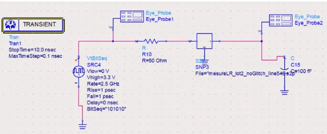
2.2.6) Transient study - Eye diagram ... 46
2.3) TSV models’ parasitic extraction ... 49
integration circuits
2.3.2) Simulation of 2 TSVs U-model ... 53
2.3.3) TSV matrix model ... 58
2.4) A 26GHz TSV based 3D filter ... 62
2.5) Conclusion ... 65
Chapter 3: Electro-thermal modeling of 3D circuits ... 66
3.1) Introduction ... 66
3.2) Electro-thermal modeling of substrate ... 67
3.2.1) Brief introduction of mathematical tools ... 67
3.2.1.1) Green Kernels ... 68
3.2.1.2) Substrate Analysis ... 68
3.2.1.3) Transmission Line Analogy for Multilayered Media ... 70
3.2.2) Simulation Results by using Green/TLM ... 73
3.2.2.1) Contacts Embedded ... 74
3.2.2.2) Alteration of the Contacts’ Shape and Their Number ... 76
3.2.3) Heat equation ... 77
3.3) Thermal connection modeling ... 82
3.3.1) 3D IC heat analysis ... 83
3.3.1.1) 3D IC heat transfer compact model without TSVs ... 83
3.3.1.2) 3D IC top layer chip temperature analysis model by considering TSVs ... 84
3.3.1.3) 3D IC Thermal modeling result ... 85
3.3.2) CMP (Chip multiprocessor) heat transfer ... 89
3.3.2.1) Thermal resistance matrix ... 91
3.3.2.2) CMP Thermal modeling result ... 91
3.3.2.3) CMP conclusion ... 94
3.4) Electro-thermal (ET) modeling of VLS circuits ... 95
3.4.1) Electrical modeling of VLS (Very Large Scale) circuits... 95
3.4.2) Electrical modeling result of 3D IC ... 96
3.4.2.1) Case I: Electrical modeling of 3xRLC segments model ... 96
3.4.2.2) Case II: CPW (Coplanar Wave Model) ... 97
3.4.2.3) Case III: Two TSVs (through silicon via) U-model ... 99
3.4.3) Thermal modeling of VLS circuits ... 104
Institut National des Sciences Appliquées de Lyon & Institut des Nanotechnologies de Lyon
3.4.4.1) Case I: One via model ... 108
3.4.4.2) Case II: One TSV model with substrate RC effect ... 112
3.4.4.3) Case III: One TSV model with a very high thermal resistance ... 114
3.5) Conclusion ... 114
Chapter 4: Heat pipe Simulation ... 116
4.1) Introduction ... 116
4.2) Configuration I & II 2D simulation ... 117
4.2.1) 2D heat pipe Analytical solution ... 117
4.2.2) FEM simulation[135] ... 121
4.2.3) Results and discussion ... 125
4.3) Configuration III 3D simulation ... 129
4.3.1) Effective thermal resistances for 3D flat heat pipes ... 129
4.3.2) Analytical solution for 3D heat pipe (configuration III) ... 133
4.3.3) Comparison results with FEM simulation ... 139
4.4) Performance-limiting Conditions ... 142
4.5) Conclusion ... 145
Chapter 5: Noise in 3D circuits ... 146
5.1) Introduction ... 146
5.2) Noise calculation using the Langevin method ... 149
5.3) Noise calculation using the impedance field method ... 153
5.4) Noise calculation using the transfer impedance method principle: formulation .... 157
5.5) Substrate noise: towards 3D ... 161
5.6) Electrical and thermo-mechanical noise impacts of through-silicon via (TSV) on transistor 162 5.6.1) Investigation method of electrical noise ... 163
5.6.2) Investigations method of thermo-mechanical noise impact ... 165
5.7) Results and discussion ... 167
5.8) Conclusion ... 172
Chapter 6: General Conclusion ... 174
Appendix A: Extraction of the CPW propagation parameters ... 177
Appendix B: Résumé en français ... 180
integration circuits
Institut National des Sciences Appliquées de Lyon & Institut des Nanotechnologies de Lyon
Chapter 1: Introduction
AI (Artificial intelligence) is a very fresh and hot topic application area that can benefit from the 3D IC. Google AlphaGo and IBM Watson’s Jeopardy defeat the best human Shogi player, but they all ran on server clusters, which are too difficult for widespread use. Today automatic driving technique uses more specialized processors, but the automobiles are not safe enough. The safety need will require more sophisticated control systems that are likely to increase computational requirements.
As we know from “von Neumann bottleneck”, data moves between the separate MPU (microprocessor unit) and memory. In this case, latency is unavoidable. These years, processor speeds have increased significantly to about 4.2 GHz. But the memory improves mostly in the density, that’s to say that the memory can store more data in a fixed space, rather than in the augmentation of transfer rates. As MPU working frequency has increased, the processor has spent an increasing amount of waiting time, in order to write and read from memory. So no matter how fast the MPU can work, it is limited by the memory transfer rate. [1], [2]
Figure 1 Performance (speed) gap between MPU and memory increasing with time[3] (Performance’s unit is number of transistors per unit cm2)
So the next generation of AI architectures is emerging the need for more densely integrated memory and processor. For example, the memory occupies a very big space in the IBM’s TrueNorth neural network chip, Google TensorFlow and the new generation of GPUs used in automatic driving cars have huge memories.
1.1) From Two-Dimension (2D) IC to Three-Dimension (3D) IC
As Figure 2a illustrates, a traditional von Neumann computer system is the heterogeneous integration of logic cells (yellow), memory chips (orange), and the interconnections (gray). For example, here Data A saves the data from RF electronics, Data B saves data from camera sensors,
integration circuits
the dynamic random-access memory (DRAM) process has a 10× higher memory density than the same generation’s logic cell. So the cache in the MPU is too small for the implementation of memory, and the data must inevitably be moved through the high-energy loss route between logic and memory, twice per communication (as shown in the green line).
Figure 2b shows the equivalent data-transmission route for one merge stage of a bitonic sort. The light yellow logic layer on top (with black points) shows the merging of four stages of bitonic sort. When applying the structure in Figure 2b, the comparisons and exchange can be placed on the logic layer. Data to be calculated (Data A) and a place of storage (Data B) are located in the bottom orange memory and connected through short wires crossing the large 2D plane, rather than a border.
(a) (b)
Figure 2 Advantage of 3D for interconnections. (a) 2D systems comprise logic and memory chips, with the green curve illustrating a mixed logic–memory calculation that’s inefficient precisely because of this logic and
memory partitioning. (b) 3D systems with tight coupling between logic and memory avoid high latency paths, bandwidth bottlenecks, and conversion of signals to high energy levels for off-chip interconnects. The blue curve
shows a representative data-movement step in sorting.
For the 3D structure in Figure 2b, data can be read all at once from memory, and then compared and exchanged in hardware. A traditional computer will need to transport all the data from memory to the processor sequentially, so, the memory bottleneck becomes a principal issue when processing a huge amount of data and other low-level kernels in artificial intelligence (AI). So the 3D circuits has a better advantage.
Moore’s Law seems to be showing down. Because of the physics limits, the technical challenges of continuously miniaturization are difficult to overcome, which is increasing the cost and slowing the pace of scaling. In addition, the benefits of scaling are decreased because of the mismatch between the scaling and the former performance advantages. So the future semiconductor industry focuses on two technical issues. Functional diversification is the first direction. It is the main driving force of System-In-Package (SiP) architecture. The second one is 3D IC, as shown in the Figure 3. This can gain the functionalities of one given node and also
Institut National des Sciences Appliquées de Lyon & Institut des Nanotechnologies de Lyon increases performance and reduces power supply. There are several driving factors for 3D integration. The benefits include better performance, reduced power supply, reduced latency, lower cost and smaller size compared to 2.5D and 2D plane packaging. Some of the basic driving factors for 3D integration are presented in the Figure 4 below.[4]
Figure 3 Elements incorporated into complex SiP packages through heterogeneous integration
Figure 4 Driving forces for 3D Integration[5], [6]
3D IC leads to a revolution of potential new scale-up. The interconnections between logic and memory has restricted systems for decades. Solving this bottleneck could continue improving system performance and advancing semiconductor industry. However, in order to get the advances, it needs some more time to work through the engineering processes (as shown in Figure 4 and Figure 5). But every little breakthrough in the engineering processes will reduce the von Neumann
integration circuits
bottleneck’s impact. For applications that could benefit from denser integration, this could offer continuous performance increases as linewidth scaling.
Figure 5 Preview of the 2017 International Roadmap for Devices and Systems’ predictions for future 3D structures. D: drain; FDSOI: fully depleted silicon on insulator; G: gate; LGAA: lateral gate-all-around; S: source;
TBOX: thin buried oxide; VGAA: vertical gate-all-around[2]
1.2) Roadmap of 3D Integrated Circuits
Computing performance can be substantially improved by monolithically integrating several new heterogeneous memory layers on top of logic layers powered by a combination of CMOS and “new switch” transistors. This new phase, called 3D power scaling, will continue to support an increase in transistor count at Moore’s law pace well into the next decade. ——Computing in science & engineering March/ April 2017, vol.19, No.2.
The 2D integration will reach the point where no more 2D scaling will be possible, the death of Moore’s law is spoken out everywhere, but the development of vertical integration of transistors and integration of layers of vertical transistors is on the way to continue increasing the transistors’ density per cm2 at a same or faster velocity than Moore’s law in the future.
The 2017 IRDS (International Roadmap for Device and System) road map projects the development of integrated-circuit technology for the next 15 years. Figure 5 offers a preview[2]. As we can see, 2D planar scaling in accordance with Moore’s law is predicted to end until the mid-2020s, after which further advances will come mainly from the stack of layers. This miniaturization will reduce die purchase fee, energy costs and operational benefits[7]. This evolution demonstrates that 3D VLSI offers the possibility to stack devices and enable high-density interconnects at device level (100 million “via” per mm2), as Table 1 shows. 3D packaging has been available for decades in large scale, with interconnections, performance, and energy efficiency. Fully integrated 3D (3D Monolithic) is supposed to be available in less than one decade.
Institut National des Sciences Appliquées de Lyon & Institut des Nanotechnologies de Lyon
Table 1 Evolution of 3D integration options toward 3D VLSI[1]
Options Links Bandwidth Latency Power Time frame
Wire-bond stack 100s Low High High Available for 30
years
Through silicon via (TSV) or
microbump stack 1,000s Medium Medium Medium
Available for 10 years
3D VLSI stack 100,000s High Low Low <10years
In the 1970s, two fundamental laws became the footstones for the whole industry: Moore’s and Dennard’s scaling laws. Dennard’s scaling law presented how to improve transistor performance by means of geometrical scaling. At the beginning of the previous decade, physical scaling (the gate oxide thickness limit) came to a halt, and the advent of new transistor by reducing the horizontal dimensions and introducing new materials and new physical effects continues the Dennard’s law. The new era is name equivalent scaling. And the vertical structures begin replace planar transistor. The predictive revolution date is 2021. At that moment, device built via 2D scaling will reach a fundamental manufacturing 2D physics limit, the transition to complete vertical device structures, heterogeneous integration in conjunction with reduced power consumption become the technology drivers.[2], [3]
Figure 6 The different ages of scaling
The IRDS projects also five steps of functional transition from 2D to 3D VLSI: (here include the functional heterogeneous devices as sensors, new storage devices, alternative logic and memory devices or circuits)
Two stacked layers with large scale components such as analog, I/O, and power management, MEMS in one layer and high-performance logic and memory in the other. Monolithic integration of two layers, where each layer contains one of the two fundamental
transistor types in logic, NMOS and PMOS (n-channel and p-channel MOS), stacked on top of each other in order to increase logic density.
integration circuits
Analog, I/O, and RF connectivity as an extra layer, giving more freedom to include special devices in the design.
3D VLSI with fine-pitch logic-on-logic as well as special functional layers exploiting new architectures
1.3) Development of 3D IC
Today, memory producers, they are facing similar problems because they have no space in 2D, and the cost of producing memory circuits of small dimensions keeps rising while the number of stored electrons in the floating gate keeps decreasing. To solve these problems, memory producers have already worked out and announced several new architectures that stack multiple layers of memory on top of each other in a single IC. As many as 48 and 96 layers of flash memory have been reported. Table 2 shows the prediction of flash memory devices for more than 100 layers. So heat removal and reduction of power will be the two main issues in the 3D power scaling.
Table 2 Flash memory trends (source: www.itrs2.net)
NAND flash
Year of production 2015 2016 2020 2022 2024 2028 2030
2D NAND flash uncontacted
poly ½ pitch-F (nm) 15 14 12 12 12 12 12
3D NAND minimum array ½
pitch-F (nm) 80nm 80nm 80nm 80nm 80nm 80nm 80nm
Number of word lines in one
3D NAND string 32 32-48 64-96 96-128 128-192 256-384 384-512
Domain cell type (FG, CT,
3D, etc.) FG/CT/3D FG/CT/3D FG/CT/3D FG/CT/3D FG/CT/3D FG/CT/3D FG/CT/3D
Product highest density (2D
or 3D) 256G 384G 768G 1T 1.5T 3T 4T
3D NAND number of
memory layers 32 32-48 64-96 96-128 128-192 256-384 384-512
Maximum number of bits per
cell for 2D NAND 3 3 3 3 3 3 3
Maximum number of bits per
cell for 3D NAND 3 3 3 3 3 3 3
Institut National des Sciences Appliquées de Lyon & Institut des Nanotechnologies de Lyon Beyond 2020, the future ICs architecture will change to a type of structure similar to the one in Figure 7. This new method of scaling, which is capable of stacking multi-layers in a 3D devices level, can substantially accelerate Moore’s law. Research on new switches began in 2005. By 2010, the tunnel FET (TFET) seems a potential replacer of MOS as shown in the figure 8, because of its lower operating power. [8] Negative capacitance FET (NC FET) has also shown as another lower operating power devise than MOS. [9], [10] CNTs (Carbon nanotube) have become the most viable switch later in the next decade, because of its energy saving and performance improvement. [11] The number of transistors that can be integrated on a cm2 of silicon will continue to increase at Moore’s law pace for the next 10 or more years by means of 3D integration. Till now, transistor speed has continued to increase during this decade, and the operation frequency of transistor has already arrived at 100 GHz if power dissipation wasn’t a bottleneck, but because of the power dissipation limits of ICs, today’s MPU’s operating frequency has been limited to a few GHz (CPU intel Core i9 4.2 GHz). So in the next decade, the goal of IC design has shifted from high frequency design to low power and better heat dissipation design.
Figure 8 Switching energy vs. delay of a 32-bit adder[12]
Three Dimensional (3D) Integration and Packaging has been successful in mainstream devices to increase logic density and to reduce data movement distances. It solves the fundamental limits of scaling e.g. increasing delay in interconnections [13], development costs and variability [14]. Most memory devices shipped today have some form of chip-stacking involved. 3D integration have different technologies, with the development, they are wire bonding and flip chip for SiP (Silicon in Package), through silicon via (TSV) in bulk, TSV in SOI (Silicon on insulator), 3D parallel, 3D sequential (MIV monolithic inter via).
integration circuits
In the bulk level design (>2um), there have two stacked dies types, the interconnection via substrate, and direct connection between dice. The typical interconnection via substrate technology is wire-bonding stack. The wire bonding stack, as shown in the Figure 10(a), has a low density, low bandwidth, high latency and high power dissipation characteristic (the exact numbers can be found in the previous table 1). And TSV in bulk is the typical one of the direct connection between dice, which is the main stream of 3D interconnection because that they don’t need substantial change to the existing fabrication flow, as shown in the Figure 10(b). The size in CMOS image sensors using “via last” approach has a diameter of about 50um. [15]–[19]. And it has smaller size for 3D stacked memory (NAND, DRAM …) and logic circuits (MPUs with cache memory). Stacking involves drilling holes through silicon chips to provide electrical connections between layers of stacked silicon chips. Chip stacks up to 40 layers deep are available that have lower engineering costs than adding layers lithographically or epitaxial deposition. TSV offers lower bandwidth and less efficient connectivity between chip layers than adding layers with photolithography processes, but far higher bandwidth and efficiency than using conventional chip packaging. It has an advantage of 10X more links in the circuit and better bandwidth, better latency, lower power supply[16], [20]–[22]. However, the keep-out zone (KOZ) [23]–[28] required for through-silicon via (TSVs) and limitations on the die alignment precision generate limits on the device integration density that can be designed using TSV-based 3D stacking [2], [26].
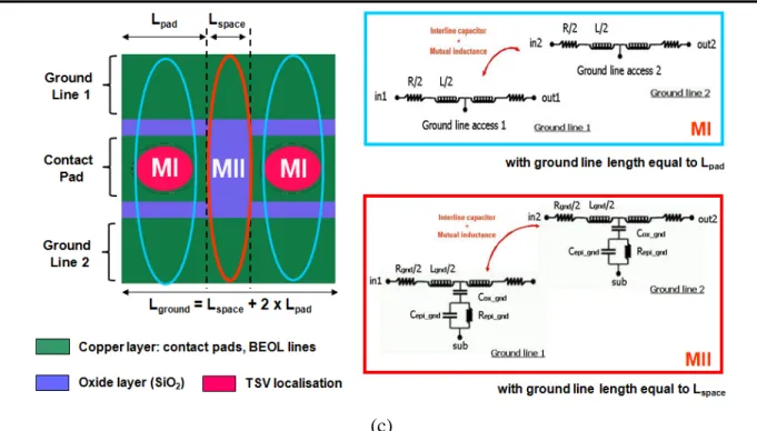
Figure 9 Alignment capability versus 3D contact width in parallel and sequential integration schemes[29]
Below 1um, in this field, the 3D technology’s interest stays at the transistor scale design. As observed in the Figure 9, which shows the alignment accuracy between the stacked transistor layers with regards to the 3D contact width (pitch), the 3D parallel integration [30], [31] as shown in the Figure 10(c), enables the continuously reduction after 3D TSV, the pitch reduction has been reduced to 1um. But even though some 3D SOI (silicon on insulator) architectures can reduce the
Institut National des Sciences Appliquées de Lyon & Institut des Nanotechnologies de Lyon 3D contact size, the 3D contact pitch remains however limited by the alignment performance, which is limited to about 1um, to guarantee a correct throughput.
3D sequential integration is the next generation of 3D integration technologies, it’s also named Monolithic 3D (M3D)[1]–[4], [7], [13], [15], [25], [27], [29], [32]–[60]. It has been demonstrated that 3D interconnections and planar contact pitches are matching even for advanced nodes [30] and it has the potential to achieve nano-scale device integration compared to TSV-based 3D stacking [60], and for the 3D parallel integration, one via has a connection of a few thousand transistors blocks [31], as shown in the table 3. That’s too coarse-grained compared with monolithic inter-tier vias (MIVs)[29]. So that’s why the 3D sequential integration is the only possibility to fully exploit the potential of the third dimension, especially at the transistor scale. There are three categories of M3D integration depending on the pitch of tier partitioning; transistor-level, gate-level and block-level M3D integration. In transistor-block-level M3D, P-channel transistors are placed on one tier and N-channel transistors on another tier, and connection between them is established by MIVs. In gate-level M3D, standard cells are split across multiple tiers, and inter-cell connections which cross tiers utilize MIVs. Block-level M3D design, which is the coarsest-grained design style, partitions functional blocks, and inter-block MIVs are deployed to deliver signals between functional modules in different tiers. Unfortunately, nowadays the commercial EDA tools to support 3D integration are temporally not available. So, various studies have been reported on M3D IC design using 3D commercial tools. M3D has also the disadvantage of device and interconnect performance mismatch between tiers, testing challenges, cost, etc.
Table 3 Ratio between 3D via and planar contact pitch in sequential and parallel case[29][30][42]
Parallel Sequential
Pitch 0.5um 1um 10nm
Dvia3D/DCONT,45nm 1/1000 1/10000 1/1
integration circuits
(c) (d)
Figure 10 Different 3D interconnection technologies (a) Wire-bonding (b) Through silicon via (high density TSV & Medium density TSV) (c) 3D parallel integration (d) 3D Sequential integration
Implementation of a 3D structure including CNFETs, resistive RAM (RRAM), and spin-transfer torque magnetic RAM (STT-MRAM) has already been proposed and analyzed by using N3XT (Nano-Engineered Computing Systems Technology) proposed by University of Stanford and University of California Berkeley.[61] The structure is shown in the Figure 11. The N3XT model has been demonstrated to have a 23X speedup and 37X energy reduction, that’s to say, it will have a total energy-delay product benefit of 851.[61]
Figure 11 monolithically integrated 3D system enabled by Nano-Engineered Computing Systems Technology (N3XT). On the right are the five key N3XT components. On the left are images of experimental technology demonstrations: (a) transmission electron microscopy (TEM) of a 3D resistive RAM (RRAM) for massive storage,
(b) scanning electron microscopy (SEM) of nanostructured materials for efficient heat removal (left: microscale capillary advection; right: copper nano-mesh with phase-change thermal storage), and (c) SEM of a monolithic 3D chip for high-performance and energy-efficient computation. CNTs: carbon nanotubes, FETs: field-effect transistors,
Institut National des Sciences Appliquées de Lyon & Institut des Nanotechnologies de Lyon
1.4) Background and outline
This new architecture shows that computing performance can still be improved in the next decade, and the main power will rely on 3D heterogeneous integration. So the future of semiconductor industry is quite bright, and future discoveries will continue to bring progress and bring new breakthrough.
This thesis is embedded in a very vast project, driven by ST Microelectronics crolles and CEA LETI in Grenoble, and in cooperation with 3IT (Interdisciplinary Institute for Technological Innovation) and University of Sherbrooke. This project has the goal to design and produce a 3D CMOS image sensor [62], and the design of cooling system of this equipment is very important; the heat dissipation issues in the 3D CMOS image sensor can be crippling. Another demonstrator is on the way. This demonstrator (Figure 12) applies the nuclear magnetic resonance (NMR) / magnetic resonance imaging technology in the micro/nano scale. In recent years, NMR/MRI portable devices have drawn attention of numerous researcher teams. They are used for variety of applications, especially for medical diagnosis. The 3D schematic of the micro/nano MNR chip is shown in the Figure 12. This project is driven by numerous hospitals, here include hospitals in Lyon and New York[63]. As we know, the coil receiver can be easily affected by the environmental noises; moreover, its self-noise is expressed as 4kRT; R is for instance, the resistance of the coil. So, reducing the coil self-noise means to reduce this resistance. And, in the same time, the quality factor Q of the coil, defined as Q = 𝜔𝜔𝜔𝜔 𝑅𝑅⁄ , will be increased. The SNR (signal noise ratio) in the coil design can be a crippling evaluator during the miniaturization of MNR/MRI.
Figure 12 Connectivity relationship of MNR chip (TSV, RDL: Redistribution layer and circuits embedded into the substrate)
integration circuits
So the purpose of the thesis is to provide a global design method for the 3D integrated circuit in electrical, thermal, electro-thermal and also noise field. Due to the high density design of 3D IC, the passive heat management method is another important work of this thesis. Hereafter will be included simulation methods for substrate and also relative connectivity (TSV, RDL, Micro strip and circuits embedded into the substrate), thermal and electro-thermal modeling method, and also keep-out of zone calculation methods.
The chapter 2 presents some background knowledge on electrical parasitic effects of TSVs. Based on the parasitic effects, we programmed and generated in Matlab a substrate impedance extractor and a 3D TLE (3D transmission line extractor), which can automatically extract the impedance from any contacts with arbitrary shape and arbitrary material. The extractors are 100% compatible with SPICE core simulator, like ADS (Advanced design system) and can be used in the S parameters extraction and transient study in ADS. The extracted data is verified with measurement results and finite element method (FEM) simulation results. Based on the parasitic effects of TSV, a 26 GHz frequency and 2 GHz bandwidth RF filter is proposed in this work.
The chapter 3 presents the thermal and electro-thermal modeling method. So the chapter 3 implements an analytical solution for multi-layers substrate nonstationary temperature distribution. In the 3D circuits, the thermal issues are crippling issues in the 3D IC design, especially when we scale down to nanoscale. The electrical resistance increase with temperature, likewise the substrate resistance. Most of thermal simulation works are based on the steady regimes; few people work on the non-stationary case. Non-stationary effects are crippling, like hot spots, which can be enhanced by voltage ramps. We propose also a multi-layers 3D IC’s 3D heat dissipation calculation method. This method is suitable for any 3D IC. A 4 core CPU heat dissipation case is studied in this chapter. The later part of this chapter presents how the thermal simulation works. The electro-thermal simulator can be 100% compatible with SPICE (-like) simulator, and the electrical part is verified with ADS. This work constructs the framework of 3D IC electro-thermal analysis.
The chapter 4 presents the passive thermal dissipation method. As a solution to the local heat dissipation, the passive heat dissipation component, flat heat pipe (FHP) is proposed as a prospective component in the chapter 4. This chapter presents the FEM simulation approach of the FHP, and also the analytical modeling. The two results have good match, and an extensive study of the working performance’s limiting condition has also been presented in this thesis.
The chapter 5 presents the noise issues of 3D IC. We firstly propose the analytical solution for the substrates noise distribution and present noise analysis methods. And this chapter investigates also the keep-out-of-zone (KOZ) of TSV to transistor. The investigation methods of electrical noise impact and thermal-mechanical noise impact are shown in this part.
Finally, the chapter 6 summarizes the contributions of these dissertation works, drawing conclusions of the manuscript.
integration circuits
Chapter 2: Electrical modeling of TSV
Integrating multiple functional layer in a single device is a major trend in the electronics field. Therefore, requiring a higher integration degree of equipment becomes more important today. 3D-IC technology based on vertical through silicon via (TSV), has been proposed as a prospective solution to the current 3D interconnection problem. Reduction of parasitic effects, higher interconnection density, faster inter-chip communication speed and less energy consumption are the main advantages of TSV interconnection [64]. In this way, the 3D-TSV technology is considered to be the main design object of 3D highly integrated technology. In the next few years, TSV structure can flourish in the field of chips. In addition, more chips will be integrated in the 3D-IC to meet the requirements for higher bandwidth, more I / O interfaces and smaller sizes. The multi-layer TSV will be the only technology to realize this structure [65]. Therefore, there is an urgent need for multi-layer TSV electrical characteristics and coupling problems in some researches.
For 3D stacked DRAM modules, some signals can be exchanged with other different chip signals (assuming the same layout of the chip), including the read control, address bus, data bus, write control, power supply [66]. Some structures have been completed by experimental tests [67]. Although the manufacturing process gets more attention, it should also emphasize more simulation analysis. Many research work has been completed, mainly focused on the study of different electrical characteristics of TSV and calculation of TSV electrical parasitic parameters formula [68]–[71]. However, the pre-layout study of electromagnetic modeling and analysis of TSV in multilayer substrates is critical before it enters production. The crosstalk becomes a key problem in reducing the TSV performance due to the fact that the silicon substrate with conductive properties, has parasitic capacitance effects on the insulating oxide (SiO2, isolation material surrounded by the TSV) and the isolation layer formed by the TSV metallization, especially in the TSV array. Many studies have focused on TSV crosstalk problems.
2.1) Single TSV analytical approach
2.1.1) Cylindrical TSV parasitic parametersCylindrical TSV is the most common TSV structure, as shown below. We can use copper, tungsten, polycrystalline silicon and so on, as the filling material, which depends on the adequate resistivity we need. Due to the simple structure, it’s the easiest one to be simulated, so the research to this model has outdistanced the other TSV structures. And the thermal-mechanical and high-frequency characteristics are the main two emerging problems of TSV [72], [73]. And in following part, we will precisely introduce cylindrical TSV.
Institut National des Sciences Appliquées de Lyon & Institut des Nanotechnologies de Lyon
Figure 13 Cylindrical TSV
2.1.1.1) Cylindrical TSV Resistance:
In low frequency, cylindrical TSV resistance can be calculated by using the traditional wire resistance equation. When the current pass through the wire, the wire’s resistance is inverse proportional to the cross-sectional area (A), and proportional to the wire’s length, the resistance can be expressed by the following equation[46], [53], [62], [74]–[82]
𝑅𝑅 =𝜌𝜌𝜌𝜌𝐴𝐴 (2-1)
And 𝜌𝜌 is the resistivity of the wire, 𝑙𝑙 is the wire’s length, 𝐴𝐴 is the wire’s cross section area. In the integrated circuit, we use normally the copper and aluminum as the interconnection material. In 3D IC design, interconnection delay has been the major influence factor of the circuit performance, so we usually use the copper (resistivity 1.68 × 10⁻⁸Ω ∙ 𝑚𝑚) instead of the aluminum (resistivity 2.83 × 10⁻⁸Ω ∙ 𝑚𝑚) to reduce the interconnection delay of via. For TSV radius 𝑟𝑟𝑇𝑇𝑇𝑇𝑇𝑇, cross sectional area π𝑟𝑟𝑇𝑇𝑇𝑇𝑇𝑇2 ’s cylindrical TSV, it’s resistance can be expressed as [44]
𝑅𝑅𝑇𝑇𝑇𝑇𝑇𝑇_𝐷𝐷𝐷𝐷 =π𝑟𝑟𝜌𝜌𝑙𝑙𝑇𝑇𝑇𝑇𝑇𝑇 𝑇𝑇𝑇𝑇𝑇𝑇
2 (2-2)
With the augmentation of the signal’s frequency, the skin effects should be taken into consideration, that’s to say, with the increase of the signal frequency in the metal, the current that passes through the via will tend to the conductor’s surface. The skin effect will increase the effective resistance of the conductor and the skin effect will be more obvious as the frequency gets higher. And here we should introduce skin depth δ. It means that when the current density in the conductor gets down to the 1
e (e: Euler’s number) times of the conductor’s surface current density,
the expression equation is [20]
δ = �𝜋𝜋𝜋𝜋𝜇𝜇𝜌𝜌0𝜇𝜇𝑚𝑚 (2-3) Here, 𝑓𝑓 is signal’s frequency of the wire, 𝜇𝜇0 is the free space permeability (the value is 4π × 10−7H/𝑚𝑚), 𝜇𝜇
𝑚𝑚 is the metal’s permeability. And through this equation, we can deduce the corner
integration circuits 𝑓𝑓𝛿𝛿=𝜋𝜋𝜇𝜇 𝜌𝜌
0𝜇𝜇𝑚𝑚𝑟𝑟𝑇𝑇𝑇𝑇𝑇𝑇2 (2-4)
So when the frequency 𝑓𝑓 is smaller than the 𝑓𝑓𝛿𝛿, the skin depth 𝛿𝛿 will be bigger than the TSV radius 𝑟𝑟𝑇𝑇𝑇𝑇𝑇𝑇 of metal part, and at this case, the skin effect is negligible. So the resistance of TSV can be defined as a DC resistance, which can be expressed as shown in the RTSV_DC=πrρlTSV
TSV
2
(2-2); when the frequency 𝑓𝑓 is bigger than the 𝑓𝑓𝛿𝛿, the skin depth 𝛿𝛿 will be smaller than the TSV radius 𝑟𝑟𝑇𝑇𝑇𝑇𝑇𝑇, and at this case, the AC resistance introduced by the skin effect can be shown as
following [83] 𝑅𝑅𝑇𝑇𝑇𝑇𝑇𝑇_𝐴𝐴𝐷𝐷=𝜋𝜋[𝑟𝑟 𝜌𝜌𝑙𝑙𝑇𝑇𝑇𝑇𝑇𝑇
𝑇𝑇𝑇𝑇𝑇𝑇
2 −(𝑟𝑟𝑇𝑇𝑇𝑇𝑇𝑇−𝛿𝛿)2] (2-5)
As we can see here, the TSV parasitic resistance is composed of a DC resistance and a AC resistance, and can be expressed as following [83]
𝑅𝑅𝑇𝑇𝑇𝑇𝑇𝑇 =�𝑅𝑅𝑇𝑇𝑇𝑇𝑇𝑇_𝐷𝐷𝐷𝐷2 + 𝑅𝑅𝑇𝑇𝑇𝑇𝑇𝑇_𝐴𝐴𝐷𝐷2 (2-6)
For a TSV with 60𝜇𝜇𝑚𝑚 diameter and 100𝑛𝑛𝑚𝑚 oxide layer thickness, the corner frequency can be 4.7 MHz, and for a TSV with 5𝜇𝜇𝑚𝑚 diameter and 100𝑛𝑛𝑚𝑚 oxide layer thickness, the corner frequency can be 681 MHz. So here means, if we don’t want to see the skin effect, either use a conductive material with a higher conductivity or reduce the via’s diameter.
2.1.1.2) Cylindrical TSV Capacitance:
The capacitance of TSV is defined as the capacitance between the metal conductor and silicon substrate, because the TSV insulation layer’s thickness is usually less than 1µm, so this parasitic capacitance has a great influence to the transmission, in the study of 3D IC signal integrity and power dissipation, TSV’s capacitance need more accurate simulation and analysis. Because of the insulation layer (𝑇𝑇𝑆𝑆𝑆𝑆2), which is used to insulate the TSV signal and the outside silicon substrate, the TSV structure forms a metal-oxide-semiconductor structure, which is MOS structure. We can get the analytical solution by solving the 1D poison equation in the cylindrical coordinate system. The TSV equivalent capacitance is composed of two parts, they are respectively oxide capacitance 𝐷𝐷𝑜𝑜𝑜𝑜 and capacitance of depletion 𝐷𝐷𝑑𝑑𝑑𝑑𝑑𝑑.
𝐷𝐷𝑜𝑜𝑜𝑜 is expressed as [84]
𝐷𝐷𝑜𝑜𝑜𝑜=ln (2𝜋𝜋𝜀𝜀𝑑𝑑𝑇𝑇𝑇𝑇𝑇𝑇+2𝑡𝑡𝑜𝑜𝑜𝑜0𝜀𝜀𝑜𝑜𝑜𝑜𝑙𝑙𝑇𝑇𝑇𝑇𝑇𝑇
𝑑𝑑𝑇𝑇𝑇𝑇𝑇𝑇 ) (2-7)
Here, 𝑡𝑡𝑜𝑜𝑜𝑜 is the thickness of the oxide layer, 𝜀𝜀𝑜𝑜𝑜𝑜 is the dielectric constant of 𝑇𝑇𝑆𝑆𝑆𝑆2 (the value is 3.9), 𝜀𝜀0 is the free space absolute dielectric constant (the value is 8.854 × 10⁻¹²F/𝑚𝑚)
Institut National des Sciences Appliquées de Lyon & Institut des Nanotechnologies de Lyon 𝐷𝐷𝑑𝑑𝑑𝑑𝑑𝑑= 2𝜋𝜋𝜀𝜀0𝜀𝜀𝑜𝑜𝑜𝑜𝑙𝑙𝑇𝑇𝑇𝑇𝑇𝑇
ln (𝑑𝑑𝑇𝑇𝑇𝑇𝑇𝑇+2𝑡𝑡𝑜𝑜𝑜𝑜+𝑊𝑊𝑑𝑑𝑑𝑑𝑑𝑑𝑑𝑑𝑇𝑇𝑇𝑇𝑇𝑇+2𝑡𝑡𝑜𝑜𝑜𝑜 ) (2-8)
And the depletion width 𝑊𝑊𝑑𝑑𝑑𝑑𝑑𝑑 can be calculated by the following relationship. [85]
𝑊𝑊𝑑𝑑𝑑𝑑𝑑𝑑=�
4𝜀𝜀0𝜀𝜀𝑠𝑠𝑆𝑆𝑇𝑇𝑡𝑡ℎln (𝑁𝑁𝐴𝐴𝑛𝑛𝑆𝑆)
𝑞𝑞𝑁𝑁𝐴𝐴 (2-9)
Here, 𝑁𝑁𝐴𝐴 is the doping density, 𝑛𝑛𝑖𝑖 is the intrinsic silicon carrier concentration (the value is 1.5 × 10¹⁶𝑚𝑚−3), 𝑇𝑇
𝑡𝑡ℎ is the thermal voltage, which can be expressed by the following equation [85]
𝑇𝑇𝑡𝑡ℎ=𝑘𝑘𝑇𝑇𝑞𝑞 (2-10) When T=300K, 𝑇𝑇𝑡𝑡ℎ’s value is 25.9mV, the 𝑘𝑘 is the Boltzmann constant (the value is 1.38 × 10⁻²³𝐽𝐽/𝐾𝐾), 𝑞𝑞 is the unit electron charge constant (the value is 1.6 × 10⁻¹⁹𝐷𝐷).
When the metal voltage and silicon substrate voltage are different, there will be MOS effect. In the analysis of the MOS effect, we should define the bias voltage, threshold voltage and flat band voltage. When the TSV is working, the voltage applied in the metal is called bias voltage of TSV (𝑇𝑇𝐵𝐵); the threshold voltage (𝑇𝑇𝑇𝑇𝑇𝑇) is the voltage applied in the metal when the voltage in the 𝑇𝑇𝑆𝑆/𝑇𝑇𝑆𝑆𝑆𝑆2 interface equals to 2ln (𝑁𝑁𝐴𝐴/𝑛𝑛𝑖𝑖); And the flat band voltage (𝑇𝑇𝐹𝐹𝐵𝐵) is the voltage applied in the metal when the 𝑇𝑇𝑆𝑆/𝑇𝑇𝑆𝑆𝑆𝑆2 turns to the flat band state, and the 𝑇𝑇𝐹𝐹𝐵𝐵 can be expressed in the following expression [85]
𝑇𝑇𝐹𝐹𝐹𝐹= Φ𝑚𝑚− Φ𝑠𝑠𝑆𝑆−𝑟𝑟𝜀𝜀𝑜𝑜𝑜𝑜𝑜𝑜𝑜𝑜𝑞𝑞Q𝜀𝜀0𝑓𝑓ln (𝑑𝑑𝑑𝑑𝑇𝑇𝑇𝑇𝑇𝑇𝑜𝑜𝑜𝑜) (2-11)
Here, Φ𝑚𝑚 is the work function of TSV’s metal conductor, Φ𝑠𝑠𝑖𝑖 is the work function of the outside silicon substrate, Q𝜋𝜋 is the surface charge of the 𝑇𝑇𝑆𝑆/𝑇𝑇𝑆𝑆𝑆𝑆2 interface.
If the silicon substrate is P type substrate, when the metal’s voltage is different from the silicon substrate, a lot of cavities will leave 𝑇𝑇𝑆𝑆/𝑇𝑇𝑆𝑆𝑆𝑆2 interface, and then the carrier depletion appears. The following Figure 14 is the MOS structure, 𝑟𝑟𝑑𝑑𝑑𝑑𝑑𝑑 is the depletion radius, 𝑟𝑟𝑜𝑜𝑜𝑜 is the oxide radius, 𝑟𝑟𝑇𝑇𝑇𝑇𝑇𝑇 is the metal’s radius.
integration circuits
When 𝑇𝑇𝐵𝐵< 𝑇𝑇𝐹𝐹𝐵𝐵, there will be depletion layer, and at this case, 𝑟𝑟𝑑𝑑𝑑𝑑𝑑𝑑 equals to the 𝑟𝑟𝑜𝑜𝑜𝑜. And this area is named accumulation region, and the equivalent capacitance is 𝐷𝐷𝑜𝑜𝑜𝑜.The expression is the same like (2-7).
𝐷𝐷𝑜𝑜𝑜𝑜=ln (2𝜋𝜋𝜀𝜀𝑑𝑑𝑇𝑇𝑇𝑇𝑇𝑇+2𝑡𝑡𝑜𝑜𝑜𝑜0𝜀𝜀𝑜𝑜𝑜𝑜𝑙𝑙𝑇𝑇𝑇𝑇𝑇𝑇
𝑑𝑑𝑇𝑇𝑇𝑇𝑇𝑇 ) (2-12)
When 𝑇𝑇𝐹𝐹𝐵𝐵≤ 𝑇𝑇𝐵𝐵< 𝑇𝑇𝑇𝑇ℎ, the depletion layer appears, with the increase of 𝑇𝑇𝐵𝐵, the 𝑊𝑊𝑑𝑑𝑑𝑑𝑑𝑑 increases,
but 𝐷𝐷𝑑𝑑𝑑𝑑𝑑𝑑 decreases (see equation (2-8) and (2-9)). And this area is named depletion region, and the
total capacitance is defined as following [85]
𝐷𝐷𝑑𝑑𝑑𝑑𝑑𝑑= 2𝜋𝜋𝜀𝜀0𝜀𝜀𝑠𝑠𝑆𝑆𝑙𝑙𝑇𝑇𝑇𝑇𝑇𝑇 ln (𝑑𝑑𝑇𝑇𝑇𝑇𝑇𝑇+2𝑡𝑡𝑜𝑜𝑜𝑜+2𝑊𝑊𝑑𝑑𝑑𝑑𝑑𝑑𝑑𝑑𝑇𝑇𝑇𝑇𝑇𝑇+2𝑡𝑡𝑜𝑜𝑜𝑜 ) (2-13) 𝑊𝑊𝑑𝑑𝑑𝑑𝑑𝑑=� 4𝜀𝜀𝑠𝑠𝑆𝑆𝑇𝑇𝐹𝐹ln (𝑁𝑁𝐴𝐴𝑛𝑛𝑆𝑆) 𝑞𝑞𝑁𝑁𝐴𝐴 (2-14) 𝐷𝐷𝑇𝑇𝑇𝑇𝑇𝑇 = (𝐷𝐷1𝑜𝑜𝑜𝑜+𝐷𝐷𝑑𝑑𝑑𝑑𝑑𝑑1 ) −1 = 𝐷𝐷𝑜𝑜𝑜𝑜𝐷𝐷𝑑𝑑𝑑𝑑𝑑𝑑 𝐷𝐷𝑜𝑜𝑜𝑜+𝐷𝐷𝑑𝑑𝑑𝑑𝑑𝑑 (2-15)
When 𝑇𝑇𝐵𝐵≥ 𝑇𝑇𝑇𝑇ℎ, the depletion width 𝑊𝑊𝑑𝑑𝑑𝑑𝑑𝑑 gets to its maximum, and it will not continue to increase with 𝑇𝑇𝐵𝐵, and this area is named inversion region, and at this moment, 𝐷𝐷𝑑𝑑𝑑𝑑𝑑𝑑 gets to its minimum, so the same as the 𝐷𝐷𝑇𝑇𝑇𝑇𝑇𝑇. [85]
𝐷𝐷𝑑𝑑𝑑𝑑𝑑𝑑= 2𝜋𝜋𝜀𝜀0𝜀𝜀𝑠𝑠𝑆𝑆𝑙𝑙𝑇𝑇𝑇𝑇𝑇𝑇 ln (𝑑𝑑𝑇𝑇𝑇𝑇𝑇𝑇+2𝑡𝑡𝑜𝑜𝑜𝑜+2𝑊𝑊𝑑𝑑𝑑𝑑𝑑𝑑 𝑑𝑑𝑇𝑇𝑇𝑇𝑇𝑇+2𝑡𝑡𝑜𝑜𝑜𝑜 ) (2-16) 𝑊𝑊𝑑𝑑𝑑𝑑𝑑𝑑 =� 4𝜀𝜀𝑠𝑠𝑆𝑆𝑇𝑇𝑡𝑡ℎln (𝑁𝑁𝐴𝐴𝑛𝑛𝑆𝑆) 𝑞𝑞𝑁𝑁𝐴𝐴 =� 4𝜀𝜀𝑠𝑠𝑆𝑆𝑘𝑘𝑇𝑇ln (𝑁𝑁𝐴𝐴𝑛𝑛𝑆𝑆) 𝑞𝑞2𝑁𝑁 𝐴𝐴 (2-17) 𝐷𝐷𝑇𝑇𝑇𝑇𝑇𝑇𝑚𝑚𝑆𝑆𝑛𝑛= (𝐷𝐷1𝑜𝑜𝑜𝑜+𝐷𝐷𝑑𝑑𝑑𝑑𝑑𝑑𝑚𝑚𝑆𝑆𝑛𝑛1 ) −1 = 𝐷𝐷𝑜𝑜𝑜𝑜𝐷𝐷𝑑𝑑𝑑𝑑𝑑𝑑𝑚𝑚𝑆𝑆𝑛𝑛 𝐷𝐷𝑜𝑜𝑜𝑜+𝐷𝐷𝑑𝑑𝑑𝑑𝑑𝑑𝑚𝑚𝑆𝑆𝑛𝑛 (2-18) 𝑇𝑇𝑇𝑇ℎ= 𝑇𝑇𝐹𝐹𝐹𝐹+ 2𝑇𝑇𝑇𝑇ln�𝑁𝑁𝑛𝑛𝑎𝑎𝑆𝑆�+𝑞𝑞𝑁𝑁𝑎𝑎𝜋𝜋(� 𝑑𝑑𝑡𝑡𝑠𝑠𝑡𝑡 2 +𝑡𝑡𝑜𝑜𝑜𝑜+𝑊𝑊𝑑𝑑𝑑𝑑𝑑𝑑� 2 −(𝑑𝑑𝑡𝑡𝑠𝑠𝑡𝑡2 +𝑡𝑡𝑜𝑜𝑜𝑜) 2 )𝑠𝑠𝑆𝑆𝑛𝑛𝑠𝑠 2𝜋𝜋𝜀𝜀𝑜𝑜𝑜𝑜 ln ( 𝑑𝑑𝑡𝑡𝑠𝑠𝑡𝑡+2𝑡𝑡𝑜𝑜𝑜𝑜+𝑙𝑙𝑡𝑡𝑠𝑠𝑡𝑡𝑐𝑐𝑜𝑜𝑡𝑡𝑠𝑠 𝑑𝑑𝑡𝑡𝑠𝑠𝑡𝑡+𝑙𝑙𝑡𝑡𝑠𝑠𝑡𝑡𝑐𝑐𝑜𝑜𝑡𝑡𝑠𝑠 ) (2-19)
Based on the TSV RC parasitic parameters’ extraction model, the paper [86] gives a TSV RC parameters’ extraction and Q3D simulation result in the 45nm CMOS background, as shown in the table below. The comparison shows that the average error between these parasitic parameters and Q3D simulation is about 5%, and the formulas can be used in TSV parasitic extractions.
Institut National des Sciences Appliquées de Lyon & Institut des Nanotechnologies de Lyon
Table 4 Different aspect ratio TSV RC parasitic parameters extraction comparison result in 45nm CMOS process from [86] Aspect ratio 1 3 5 Diameter d/um 5 Tox /nm 120 NA /cm3 2E15 Theorical resistance/mOhm 0.30 2.80 1.40 Q3D Resistance/mOhm 0.35 3.03 1.75 Resistance error/% 1.15 1.77 1.61 Theorical capacitor/fF 0.14 7.43 5.71 Q3D capacitor/fF 0.38 8.28 7.21 Capacitor error/% 2.56 3.10 3.28 2.1.1.3) Cylindrical TSV Inductance
The TSV’s inductance is composed of self-inductance and mutual-inductance, here we use some simplifications, and assume that the current back path is in the infinite, so the inductance of TSV is, (𝑑𝑑𝑇𝑇𝑇𝑇𝑇𝑇 is the TSV’s metal diameter), this formulae comes from publication [87] by taking taper angle to 0. 𝜔𝜔𝑇𝑇𝑇𝑇𝑇𝑇 = 𝜔𝜔𝑆𝑆𝑛𝑛𝑛𝑛𝑑𝑑𝑟𝑟+ 𝜔𝜔𝑑𝑑𝑜𝑜𝑡𝑡=𝜇𝜇0𝜇𝜇8𝜋𝜋𝑚𝑚𝑙𝑙𝑇𝑇𝑇𝑇𝑇𝑇+𝜇𝜇02𝜋𝜋𝜇𝜇𝑚𝑚𝑙𝑙𝑇𝑇𝑇𝑇𝑇𝑇[ln�2𝑙𝑙𝑇𝑇𝑇𝑇𝑇𝑇+�𝑑𝑑𝑇𝑇𝑇𝑇𝑇𝑇 2 +4𝑙𝑙 𝑇𝑇𝑇𝑇𝑇𝑇 2 𝑑𝑑𝑇𝑇𝑇𝑇𝑇𝑇 �+ (𝑑𝑑𝑇𝑇𝑇𝑇𝑇𝑇− �𝑑𝑑𝑇𝑇𝑇𝑇𝑇𝑇2 + 4𝑙𝑙𝑇𝑇𝑇𝑇𝑇𝑇2 )] (2-20)
Normally the inner inductance is far smaller than the exterior inductance, so the inductance of TSV can be expressed as [87] 𝜔𝜔𝑇𝑇𝑇𝑇𝑇𝑇 =𝜇𝜇02𝜋𝜋𝜇𝜇𝑚𝑚𝑙𝑙𝑇𝑇𝑇𝑇𝑇𝑇[ln � 2𝜌𝜌𝑇𝑇𝑇𝑇𝑇𝑇+�𝑑𝑑𝑇𝑇𝑇𝑇𝑇𝑇2 +4𝜌𝜌𝑇𝑇𝑇𝑇𝑇𝑇2 𝑑𝑑𝑇𝑇𝑇𝑇𝑇𝑇 � + (𝑑𝑑𝑇𝑇𝑇𝑇𝑇𝑇− �𝑑𝑑𝑇𝑇𝑇𝑇𝑇𝑇 2 + 4𝑙𝑙 𝑇𝑇𝑇𝑇𝑇𝑇 2 )] (2-21)
Table 5 Different size TSV inductance
TSV diameter TSV height TSV oxide thickness Ltsv
2um 20um 0.05um 13.827pH
2um 20um 0.1um 14.049pH
5um 20um 0.05um 10.185pH
5um 20um 0.1um 10.262pH
integration circuits 2.1.1.4) Interconnection delay
Due to the longer and longer interconnection delay, it will decide the limit between system clock frequency and interconnection transmission. In order to reduce the interconnection RC delay, paper [86] propose a buffer inserted design.
Figure 15 Interconnection model after inserting buffer
Figure 15 shows the interconnection model after inserting buffer, in the Figure 15, r and c are respectively the interconnection resistance and capacitance per unit length. The equivalent buffer resistance can be expressed as 𝑅𝑅𝑑𝑑/𝑠𝑠𝑜𝑜𝑑𝑑𝑡𝑡, and equivalent capacitance can be expressed as 𝐷𝐷0∗ 𝑠𝑠𝑜𝑜𝑑𝑑𝑡𝑡,
𝑠𝑠𝑜𝑜𝑑𝑑𝑡𝑡 and 𝜔𝜔𝑜𝑜𝑑𝑑𝑡𝑡 are the buffer’s best size and distance, 𝑅𝑅𝑑𝑑 and 𝐷𝐷0 are respectively the buffer’s output
resistance and input capacitance. And the longest interconnection delay 𝐷𝐷𝑟𝑟𝑑𝑑𝑑𝑑 can be expressed as following [88]
𝐷𝐷𝑟𝑟𝑑𝑑𝑑𝑑= 2.37𝜔𝜔𝑙𝑙𝑜𝑜𝑛𝑛𝑙𝑙𝑑𝑑𝑠𝑠𝑡𝑡�𝑅𝑅𝑑𝑑𝐷𝐷0𝑟𝑟𝑐𝑐 (2-22)
And 𝜔𝜔𝜌𝜌𝑜𝑜𝑙𝑙𝑙𝑙𝑑𝑑𝑠𝑠𝑡𝑡 is the overall longest interconnection line, and it can be expressed by the Davis
random distribution model. [88]
𝜔𝜔𝑙𝑙𝑜𝑜𝑛𝑛𝑙𝑙𝑑𝑑𝑠𝑠𝑡𝑡 = 2��𝑁𝑁𝑇𝑇𝑡𝑡− 1�+ 𝑚𝑚(𝑇𝑇 − 1) (2-23)
𝑁𝑁𝑡𝑡 is the chip’s total logic gate number, 𝑇𝑇 is the silicon source layers number, 𝑚𝑚 is the ratio
between layer distance and gate distance. If 𝑁𝑁𝑡𝑡 ≫ 𝑚𝑚, 𝜔𝜔𝜌𝜌𝑜𝑜𝑙𝑙𝑙𝑙𝑑𝑑𝑠𝑠𝑡𝑡 ∝ 1
√𝑇𝑇, so by reducing the silicon
source layers number, it can reduce the time delay. But with the increase of the integration density, TSV RC delay becomes necessary. TSV’s equivalent lumped II style RC model can be written as: [88]
𝐷𝐷3𝐷𝐷= 𝐷𝐷𝑟𝑟𝑑𝑑𝑑𝑑+ 𝑁𝑁𝑇𝑇𝑇𝑇𝑇𝑇∗ 𝐷𝐷𝑇𝑇𝑇𝑇𝑇𝑇 (2-24)
And here 𝑁𝑁𝑇𝑇𝑇𝑇𝑇𝑇 is the chip’s TSV numbers along the interconnection line. And the buffer’s TSV intrinsic delay is [88]
𝐷𝐷𝑇𝑇𝑇𝑇𝑇𝑇 =𝑠𝑠𝑅𝑅𝑜𝑜𝑑𝑑𝑡𝑡𝑑𝑑 ⋅𝐷𝐷𝑇𝑇𝑇𝑇𝑇𝑇2 + (𝑠𝑠𝑅𝑅𝑜𝑜𝑑𝑑𝑡𝑡𝑑𝑑 + 𝑅𝑅𝑇𝑇𝑇𝑇𝑇𝑇) × (𝐷𝐷𝑇𝑇𝑇𝑇𝑇𝑇2 + 𝑠𝑠𝑜𝑜𝑑𝑑𝑡𝑡𝐷𝐷0) (2-25) 2.1.1.5) Power dissipation during interconnection
Institut National des Sciences Appliquées de Lyon & Institut des Nanotechnologies de Lyon
𝑃𝑃𝑡𝑡𝑜𝑜𝑡𝑡𝑎𝑎𝑙𝑙= 𝑃𝑃𝑆𝑆𝑛𝑛𝑡𝑡+ 𝑃𝑃𝑙𝑙𝑜𝑜𝑙𝑙𝑆𝑆𝑐𝑐+ 𝑃𝑃𝑟𝑟𝑑𝑑𝑑𝑑+ 𝑃𝑃𝑇𝑇𝑇𝑇𝑇𝑇 (2-26)
Here 𝑃𝑃𝑖𝑖𝑙𝑙𝑡𝑡 is the interconnection line dissipation, 𝑃𝑃𝜌𝜌𝑜𝑜𝑙𝑙𝑖𝑖𝑙𝑙 is the logic gate dissipation, 𝑃𝑃𝑟𝑟𝑑𝑑𝑑𝑑 is the inserted buffer dissipation, 𝑃𝑃𝑇𝑇𝑇𝑇𝑇𝑇 is the TSV dissipation.
𝑃𝑃𝑆𝑆𝑛𝑛𝑡𝑡=𝑠𝑠2𝐷𝐷𝑆𝑆𝑛𝑛𝑡𝑡𝜔𝜔𝑡𝑡𝑜𝑜𝑡𝑡𝑇𝑇𝑑𝑑𝑑𝑑2 𝑓𝑓 (2-27)
Here, 𝑇𝑇𝑑𝑑𝑑𝑑 is the supply voltage, 𝑠𝑠 is the average gate active factor, 𝑓𝑓 is the working frequency,
𝐷𝐷𝑖𝑖𝑙𝑙𝑡𝑡 is the interconnection capacitance per unit length, 𝜔𝜔𝑡𝑡𝑜𝑜𝑡𝑡 is the total length of interconnection
line, it’s supposed to follow the random distribution model. [89], [90]
𝜔𝜔𝑡𝑡𝑜𝑜𝑡𝑡 =∫12�𝑁𝑁𝑡𝑡𝑙𝑙 ∙ 𝑆𝑆(𝑙𝑙)𝑑𝑑𝑙𝑙 (2-28)
𝑆𝑆(𝑙𝑙) is the interconnection density function.
Logic gate and inserted buffer have the same dissipation model, they can be expressed as [89], [90]
𝑃𝑃𝑙𝑙𝑜𝑜𝑙𝑙𝑆𝑆𝑐𝑐= 𝑁𝑁𝑡𝑡𝑠𝑠2𝐷𝐷𝑙𝑙𝑜𝑜𝑙𝑙𝑆𝑆𝑐𝑐𝑇𝑇𝑑𝑑𝑑𝑑2 𝑓𝑓 (2-29)
𝑃𝑃𝑟𝑟𝑑𝑑𝑑𝑑= 𝑛𝑛𝑟𝑟𝑑𝑑𝑑𝑑𝑠𝑠2𝐷𝐷𝑟𝑟𝑑𝑑𝑑𝑑𝑇𝑇𝑑𝑑𝑑𝑑2 𝑓𝑓 (2-30)
𝐷𝐷𝜌𝜌𝑜𝑜𝑙𝑙𝑖𝑖𝑙𝑙 and 𝐷𝐷𝑟𝑟𝑑𝑑𝑑𝑑 are respectively the gate and buffer’s equivalent capacitance, 𝑛𝑛𝑟𝑟𝑑𝑑𝑑𝑑 is the
inserted buffer’s number and 𝑁𝑁𝑡𝑡 is the chip’s total logic gate number. And the TSV’s RC model depends on the via’s number. [89], [90]
𝑃𝑃𝑇𝑇𝑇𝑇𝑇𝑇= 𝑁𝑁𝑇𝑇𝑇𝑇𝑇𝑇𝑠𝑠2𝐷𝐷𝑇𝑇𝑇𝑇𝑇𝑇𝑇𝑇𝑑𝑑𝑑𝑑2 𝑓𝑓 (2-31)
2.1.2) Taper TSV parasitic parameters
Taper TSV is proposed by MIT’s Lincoln’s laboratory[47], its structure is shown as Figure 16. Taper TSV is an inevitable manufacturing byproduct, due to the non-ideal Dry Reactive Ion Etching[91]. Paper[92] proposed a precisely controlled taper TSV fabrication process. But in compare with the cylindrical TSV, taper TSV has a higher parasitic resistance. And if it has a very high inclination, it’s easy to generate a ‘V’ form TSV (which will be an error).[88]–[101]
integration circuits
Figure 16 Taper TSV
2.1.2.1) Taper TSV Resistance:
Taper TSV resistance is also composed with a DC part and AC part[87].
𝑅𝑅𝑇𝑇𝑇𝑇𝑇𝑇_𝐷𝐷𝐷𝐷=𝜋𝜋𝑎𝑎(𝑎𝑎+𝑙𝑙𝜌𝜌𝑙𝑙𝑇𝑇𝑇𝑇𝑇𝑇𝑇𝑇𝑇𝑇𝑇𝑇𝛽𝛽)[1 +12𝛽𝛽2] (2-32) δ = �𝜋𝜋𝜋𝜋𝜇𝜇𝜌𝜌0𝜇𝜇𝑚𝑚 (2-33) 𝑓𝑓𝛿𝛿=𝜋𝜋𝜇𝜇 𝜌𝜌 0𝜇𝜇𝑚𝑚𝑟𝑟𝑇𝑇𝑇𝑇𝑇𝑇2 (2-34) 𝑅𝑅𝑇𝑇𝑇𝑇𝑇𝑇_𝐴𝐴𝐷𝐷=𝜌𝜌(2+𝛽𝛽 2) 4𝜋𝜋𝛽𝛽δ log (1 + 2𝛽𝛽𝑙𝑙𝑇𝑇𝑇𝑇𝑇𝑇 2𝑎𝑎−δ) (2-35) 𝑅𝑅𝑇𝑇𝑇𝑇𝑇𝑇 =�𝑅𝑅𝑇𝑇𝑇𝑇𝑇𝑇_𝐷𝐷𝐷𝐷2 + 𝑅𝑅𝑇𝑇𝑇𝑇𝑇𝑇_𝐴𝐴𝐷𝐷2 (2-36)
Where 𝛽𝛽 = (𝑏𝑏 − 𝑎𝑎)/𝑙𝑙𝑇𝑇𝑇𝑇𝑇𝑇, 𝑏𝑏 and a are respectively top surface and bottom surface radius. When 𝛽𝛽 = 0, the model will change to cylindrical TSV model.
2.1.2.2) Taper TSV Capacitance:
When we change from cylindrical TSV to taper TSV 𝐷𝐷𝑜𝑜𝑜𝑜 will change to [87]
𝐷𝐷𝑜𝑜𝑜𝑜= 2𝜋𝜋𝜀𝜀0𝜀𝜀𝑜𝑜𝑜𝑜𝑙𝑙𝑇𝑇𝑇𝑇𝑇𝑇 sinαln (𝑑𝑑𝑇𝑇𝑇𝑇𝑇𝑇+2𝑡𝑡𝑜𝑜𝑜𝑜+𝑙𝑙𝑇𝑇𝑇𝑇𝑇𝑇𝑐𝑐𝑜𝑜𝑡𝑡𝑠𝑠
𝑑𝑑𝑇𝑇𝑇𝑇𝑇𝑇+𝑙𝑙𝑇𝑇𝑇𝑇𝑇𝑇𝑐𝑐𝑜𝑜𝑡𝑡𝑠𝑠 )
(2-37)
When 𝑠𝑠 = 90°, taper TSV will turn to a cylindrical TSV, and the formula will change back to the cylindrical TSV formulas
Institut National des Sciences Appliquées de Lyon & Institut des Nanotechnologies de Lyon 𝐷𝐷𝑑𝑑𝑑𝑑𝑑𝑑= 2𝜋𝜋𝜀𝜀0𝜀𝜀𝑜𝑜𝑜𝑜𝑙𝑙𝑇𝑇𝑇𝑇𝑇𝑇
sinαln (𝑑𝑑𝑇𝑇𝑇𝑇𝑇𝑇+2𝑡𝑡𝑜𝑜𝑜𝑜+2𝑊𝑊𝑑𝑑𝑑𝑑𝑑𝑑+𝑙𝑙𝑇𝑇𝑇𝑇𝑇𝑇𝑐𝑐𝑜𝑜𝑡𝑡𝑠𝑠𝑑𝑑𝑇𝑇𝑇𝑇𝑇𝑇+2𝑡𝑡𝑜𝑜𝑜𝑜+𝑙𝑙𝑇𝑇𝑇𝑇𝑇𝑇𝑐𝑐𝑜𝑜𝑡𝑡𝑠𝑠 ) (2-38)
And the depletion width 𝑊𝑊𝑑𝑑𝑑𝑑𝑑𝑑 can be calculated by poisson’s equation, but it’s too complicated.
𝑇𝑇𝐹𝐹𝐵𝐵 is the flat band voltage, which is the voltage applied at the via when the system stay in the
flat band state. It can be expressed as [87]
𝑇𝑇𝐹𝐹𝐹𝐹= Φ𝑚𝑚− Φ𝑇𝑇𝑆𝑆= Φ𝑚𝑚− Χ −2𝑞𝑞𝐸𝐸𝑙𝑙− V𝑇𝑇log (𝑁𝑁𝑛𝑛𝑆𝑆𝑎𝑎) (2-39)
Where Φ𝑚𝑚 is the metal’s work function, for copper, Φ𝑚𝑚 = 4.65𝑇𝑇, Φ𝑇𝑇𝑖𝑖 is the silicon substrate work function, Χ = 4.05V is the electronic affinity for silicon substrate, the intrinsic carrier concentration 𝑛𝑛𝑆𝑆 = 1.18𝑑𝑑10 𝑐𝑐𝑚𝑚−3, band gap 𝐸𝐸𝑙𝑙= 1.12𝑑𝑑𝑇𝑇, the unit charge 𝑞𝑞 = 1.6022𝑑𝑑−19𝐷𝐷, in the room temperature, the thermal voltage 𝑇𝑇𝑇𝑇=𝑘𝑘𝑇𝑇𝑞𝑞 = 0.026𝑇𝑇, 𝑁𝑁𝑎𝑎 = 1.25𝑑𝑑15𝑐𝑐𝑚𝑚−3 is the ionized acceptor concentration, 𝑄𝑄𝑓𝑓= 5𝑑𝑑14 ∗ 𝑞𝑞 C/𝑚𝑚2 is the Si/SiO2 surface charge density.
And for the 𝑊𝑊𝑑𝑑𝑑𝑑𝑑𝑑, we have the following relationship. [87]
𝑇𝑇𝑇𝑇𝑇𝑇𝑇𝑇 = V𝐹𝐹𝐹𝐹+ Ψ(𝑅𝑅𝑜𝑜𝑜𝑜)+ 𝑈𝑈𝑜𝑜𝑜𝑜 (2-40) 𝑈𝑈𝑜𝑜𝑜𝑜=𝐷𝐷𝑄𝑄𝑜𝑜𝑜𝑜𝑚𝑚 =𝑞𝑞𝑁𝑁𝑎𝑎𝜋𝜋(𝑅𝑅𝑑𝑑𝑑𝑑𝑑𝑑 2 −𝑅𝑅 𝑜𝑜𝑜𝑜 2 )𝑠𝑠𝑆𝑆𝑛𝑛𝑠𝑠 2𝜋𝜋𝜀𝜀𝑜𝑜𝑜𝑜 log ( 2𝑅𝑅𝑜𝑜𝑜𝑜+𝑙𝑙𝑡𝑡𝑠𝑠𝑡𝑡𝑐𝑐𝑜𝑜𝑡𝑡𝑠𝑠 2𝑅𝑅𝑚𝑚+𝑙𝑙𝑡𝑡𝑠𝑠𝑡𝑡𝑐𝑐𝑜𝑜𝑡𝑡𝑠𝑠) (2-41) Ψ(𝑅𝑅𝑜𝑜𝑜𝑜) =𝑞𝑞𝑁𝑁𝑎𝑎𝑅𝑅𝑜𝑜𝑜𝑜 2 4𝜀𝜀𝑠𝑠𝑠𝑠 − 𝑞𝑞𝑁𝑁𝑎𝑎𝑅𝑅𝑑𝑑𝑑𝑑𝑑𝑑2 2𝜀𝜀𝑠𝑠𝑠𝑠 log(𝑅𝑅𝑜𝑜𝑜𝑜) + 𝑞𝑞𝑁𝑁𝑎𝑎𝑅𝑅𝑑𝑑𝑑𝑑𝑑𝑑2 4𝜀𝜀𝑠𝑠𝑠𝑠 �2 log�𝑅𝑅𝑑𝑑𝑑𝑑𝑑𝑑� − 1� (2-42)
And we can get the 𝑅𝑅𝑑𝑑𝑑𝑑𝑑𝑑𝑚𝑚𝑎𝑎𝑜𝑜 by the following relationship
𝑞𝑞𝑁𝑁𝑎𝑎𝑅𝑅𝑜𝑜𝑜𝑜2 4𝜀𝜀𝑠𝑠𝑆𝑆 − 𝑞𝑞𝑁𝑁𝑎𝑎𝑅𝑅𝑑𝑑𝑑𝑑𝑑𝑑𝑚𝑚𝑎𝑎𝑜𝑜2 2𝜀𝜀𝑠𝑠𝑆𝑆 log(𝑅𝑅𝑜𝑜𝑜𝑜)+ 𝑞𝑞𝑁𝑁𝑎𝑎𝑅𝑅𝑑𝑑𝑑𝑑𝑑𝑑𝑚𝑚𝑎𝑎𝑜𝑜2 4𝜀𝜀𝑠𝑠𝑆𝑆 �2 log�𝑅𝑅𝑑𝑑𝑑𝑑𝑑𝑑𝑚𝑚𝑎𝑎𝑜𝑜�− 1�= 2𝑇𝑇𝑇𝑇log ( 𝑁𝑁𝑎𝑎 𝑛𝑛𝑆𝑆) (2-43)
And the threshold for the minimum capacitance region is 𝑇𝑇𝑡𝑡ℎ= 𝑇𝑇𝐹𝐹𝐹𝐹+ 2𝑇𝑇𝑇𝑇log�𝑁𝑁𝑛𝑛𝑆𝑆𝑎𝑎�+𝑞𝑞𝑁𝑁𝑎𝑎𝜋𝜋(𝑅𝑅𝑑𝑑𝑑𝑑𝑑𝑑𝑚𝑚𝑎𝑎𝑜𝑜 2 −𝑅𝑅 𝑜𝑜𝑜𝑜 2 )𝑠𝑠𝑆𝑆𝑛𝑛𝑠𝑠 2𝜋𝜋𝜀𝜀𝑜𝑜𝑜𝑜 log ( 2𝑅𝑅𝑜𝑜𝑜𝑜+𝑙𝑙𝑡𝑡𝑠𝑠𝑡𝑡𝑐𝑐𝑜𝑜𝑡𝑡𝑠𝑠 2𝑅𝑅𝑚𝑚+𝑙𝑙𝑡𝑡𝑠𝑠𝑡𝑡𝑐𝑐𝑜𝑜𝑡𝑡𝑠𝑠) (2-44)
When 𝑇𝑇𝐹𝐹 < 𝑇𝑇𝐹𝐹𝐹𝐹 accumulation region, there will not be depletion layer, and at this case, 𝑟𝑟𝑑𝑑𝑑𝑑𝑑𝑑 equals to the 𝑟𝑟𝑜𝑜𝑜𝑜. And this area is named accumulation region, and the equivalent capacitance is 𝐷𝐷𝑜𝑜𝑜𝑜.The expression is the same like (2-37).
𝐷𝐷𝑇𝑇𝑇𝑇𝑇𝑇= 𝐷𝐷𝑜𝑜𝑜𝑜= 2𝜋𝜋𝜀𝜀0𝜀𝜀𝑜𝑜𝑜𝑜𝑙𝑙𝑇𝑇𝑇𝑇𝑇𝑇
sinαln (𝑑𝑑𝑇𝑇𝑇𝑇𝑇𝑇+2𝑡𝑡𝑜𝑜𝑜𝑜+𝑙𝑙𝑇𝑇𝑇𝑇𝑇𝑇𝑐𝑐𝑜𝑜𝑡𝑡𝑠𝑠𝑑𝑑𝑇𝑇𝑇𝑇𝑇𝑇+𝑙𝑙𝑇𝑇𝑇𝑇𝑇𝑇𝑐𝑐𝑜𝑜𝑡𝑡𝑠𝑠 ) (2-45)
When 𝑇𝑇𝐹𝐹𝐹𝐹≤ 𝑇𝑇𝐹𝐹< 𝑇𝑇𝑇𝑇ℎ depletion region, the depletion layer appears, with the increase of 𝑇𝑇𝐹𝐹,
the 𝑊𝑊𝑑𝑑𝑑𝑑𝑑𝑑 increases, but 𝐷𝐷𝑑𝑑𝑑𝑑𝑑𝑑 decreases (see equation (2-8) and (2-9)). And this area is named
integration circuits 𝐷𝐷𝑑𝑑𝑑𝑑𝑑𝑑= 2𝜋𝜋𝜀𝜀0𝜀𝜀𝑠𝑠𝑆𝑆𝑙𝑙𝑇𝑇𝑇𝑇𝑇𝑇 sinαln (𝑑𝑑𝑇𝑇𝑇𝑇𝑇𝑇+2𝑡𝑡𝑜𝑜𝑜𝑜+2𝑊𝑊𝑑𝑑𝑑𝑑𝑑𝑑𝑑𝑑𝑇𝑇𝑇𝑇𝑇𝑇+2𝑡𝑡𝑜𝑜𝑜𝑜 ) (2-46) 𝐷𝐷𝑇𝑇𝑇𝑇𝑇𝑇 = (𝐷𝐷1𝑜𝑜𝑜𝑜+𝐷𝐷𝑑𝑑𝑑𝑑𝑑𝑑1 ) −1 = 𝐷𝐷𝑜𝑜𝑜𝑜𝐷𝐷𝑑𝑑𝑑𝑑𝑑𝑑 𝐷𝐷𝑜𝑜𝑜𝑜+𝐷𝐷𝑑𝑑𝑑𝑑𝑑𝑑 (2-47)
When 𝑇𝑇𝐹𝐹 ≥ 𝑇𝑇𝑇𝑇ℎ minimum capacitance region, the depletion width 𝑊𝑊𝑑𝑑𝑑𝑑𝑑𝑑 gets to its maximum, and it will not continue to increase with 𝑇𝑇𝐹𝐹, and this area is named inversion region, and at this moment, 𝐷𝐷𝑑𝑑𝑑𝑑𝑑𝑑 gets to its minimum, so the same as the 𝐷𝐷𝑇𝑇𝑇𝑇𝑇𝑇.
𝐷𝐷𝑑𝑑𝑑𝑑𝑑𝑑= 2𝜋𝜋𝜀𝜀0𝜀𝜀𝑠𝑠𝑆𝑆𝑙𝑙𝑇𝑇𝑇𝑇𝑇𝑇 sinαln (𝑑𝑑𝑇𝑇𝑇𝑇𝑇𝑇+2𝑡𝑡𝑜𝑜𝑜𝑜+2𝑊𝑊𝑑𝑑𝑑𝑑𝑑𝑑𝑚𝑚𝑎𝑎𝑜𝑜𝑑𝑑𝑇𝑇𝑇𝑇𝑇𝑇+2𝑡𝑡𝑜𝑜𝑜𝑜 ) (2-48) 𝐷𝐷𝑇𝑇𝑇𝑇𝑇𝑇𝑚𝑚𝑆𝑆𝑛𝑛= (𝐷𝐷1𝑜𝑜𝑜𝑜+𝐷𝐷𝑑𝑑𝑑𝑑𝑑𝑑𝑚𝑚𝑆𝑆𝑛𝑛1 ) −1 = 𝐷𝐷𝑜𝑜𝑜𝑜𝐷𝐷𝑑𝑑𝑑𝑑𝑑𝑑𝑚𝑚𝑆𝑆𝑛𝑛 𝐷𝐷𝑜𝑜𝑜𝑜+𝐷𝐷𝑑𝑑𝑑𝑑𝑑𝑑𝑚𝑚𝑆𝑆𝑛𝑛 (2-49)
As we can see, the taper TSV model has some similarities with cylindrical TSV, so it can be simplified.
𝐷𝐷𝑜𝑜𝑜𝑜_𝐷𝐷 = sinα𝐷𝐷𝑜𝑜𝑜𝑜_𝑇𝑇 (2-50)
𝐷𝐷𝑑𝑑𝑑𝑑𝑑𝑑_𝐷𝐷 = sinα𝐷𝐷𝑑𝑑𝑑𝑑𝑑𝑑_𝑇𝑇 (2-51)
So, the cylindrical and taper TSV’s parasite capacitance have the following relationship
𝐷𝐷𝑇𝑇𝑇𝑇𝑇𝑇_𝐷𝐷= sinα𝐷𝐷𝑇𝑇𝑇𝑇𝑇𝑇_𝑇𝑇 (2-52)
So if we use error to present the relative error, when 1 − sinα < 𝑑𝑑𝑟𝑟𝑟𝑟𝑜𝑜𝑟𝑟, that’s when α > 𝑎𝑎𝑟𝑟𝑐𝑐𝑠𝑠𝑆𝑆𝑛𝑛 (1 − 𝑑𝑑𝑟𝑟𝑟𝑟𝑜𝑜𝑟𝑟), the Taper TSV can use the cylindrical TSV’s model. If error = 5%, we can get the limit inclination is 73 degree. So that means if the inclination of the taper TSV is less than 15 degree, we can use the cylindrical TSV model.
2.1.2.3) Taper TSV Inductance
When the taper TSV’s inclination is less than 15 degree, the parasitic inductance can be expressed as, [87] 𝜔𝜔𝑇𝑇𝑇𝑇𝑇𝑇 =𝜇𝜇0𝜇𝜇8𝜋𝜋𝑚𝑚𝑙𝑙𝑇𝑇𝑇𝑇𝑇𝑇+𝜇𝜇0𝜇𝜇2𝜋𝜋𝑚𝑚𝑙𝑙𝑇𝑇𝑇𝑇𝑇𝑇[ln�𝑙𝑙𝑇𝑇𝑇𝑇𝑇𝑇+�𝑎𝑎 2+𝑙𝑙𝑇𝑇𝑇𝑇𝑇𝑇2 𝑎𝑎 �+�2𝑎𝑎 − 2�𝑎𝑎2+ 𝑙𝑙𝑇𝑇𝑇𝑇𝑇𝑇2 �+ 4𝛽𝛽𝑙𝑙𝑇𝑇𝑇𝑇𝑇𝑇(𝑙𝑙𝑇𝑇𝑇𝑇𝑇𝑇2 −(𝑙𝑙𝑇𝑇𝑇𝑇𝑇𝑇+𝑎𝑎)(�𝑎𝑎2+𝑙𝑙𝑇𝑇𝑇𝑇𝑇𝑇2 −𝑎𝑎)) (�𝑎𝑎2+𝑙𝑙𝑇𝑇𝑇𝑇𝑇𝑇2 −𝑙𝑙𝑇𝑇𝑇𝑇𝑇𝑇)(4𝑎𝑎+𝛽𝛽𝑙𝑙𝑇𝑇𝑇𝑇𝑇𝑇) ] (2-53)
2.1.3) Single Tapper TSV analytical result
In order to verify the taper TSV model, we use a standard TSV geometry, TSV metal radius
𝑟𝑟𝑇𝑇𝑇𝑇𝑇𝑇= 2.5𝜇𝜇𝑚𝑚, height 𝑙𝑙𝑇𝑇𝑇𝑇𝑇𝑇 = 10𝜇𝜇𝑚𝑚, oxide layer thickness 𝑡𝑡𝑜𝑜𝑜𝑜= 0.1𝜇𝜇𝑚𝑚. And here we study the
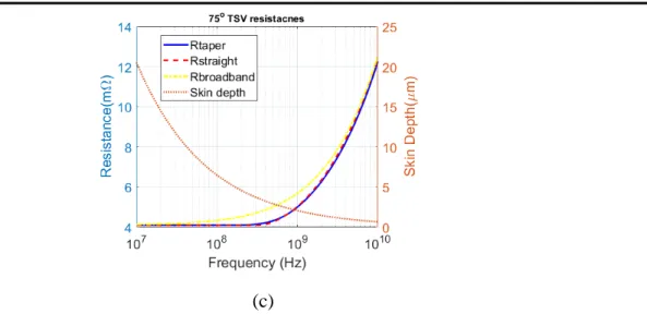
different inclination angle’s influences by considering tapper TSV skin effect. As we can see from the Figure 17, from 1MHz to 10MHz, this region is constant, this is the DC region. Beyond 1GHz,

![Figure 9 Alignment capability versus 3D contact width in parallel and sequential integration schemes[29]](https://thumb-eu.123doks.com/thumbv2/123doknet/14700445.746892/16.918.206.749.546.910/figure-alignment-capability-contact-parallel-sequential-integration-schemes.webp)
![Table 3 Ratio between 3D via and planar contact pitch in sequential and parallel case[29][30][42]](https://thumb-eu.123doks.com/thumbv2/123doknet/14700445.746892/17.918.133.818.598.953/table-ratio-between-planar-contact-pitch-sequential-parallel.webp)