RESEARCH OUTPUTS / RÉSULTATS DE RECHERCHE
Author(s) - Auteur(s) :
Publication date - Date de publication :
Permanent link - Permalien :
Rights / License - Licence de droit d’auteur :
Bibliothèque Universitaire Moretus Plantin
Institutional Repository - Research Portal
Dépôt Institutionnel - Portail de la Recherche
researchportal.unamur.be
University of Namur
In-depth investigation of the charge extraction efficiency for thermally annealed inverted bulk-heterojunction solar cells
Kolb, Florian; Busby, Yan; Houssiau, Laurent; J.W. List-Kratchvil, Emil Published in:
Journal of Applied Physics DOI:
10.1063/1.5052409
Publication date: 2019
Document Version Peer reviewed version Link to publication
Citation for pulished version (HARVARD):
Kolb, F, Busby, Y, Houssiau, L & J.W. List-Kratchvil, E 2019, 'In-depth investigation of the charge extraction efficiency for thermally annealed inverted bulk-heterojunction solar cells', Journal of Applied Physics, vol. 125, no. 3, 034502. https://doi.org/10.1063/1.5052409
General rights
Copyright and moral rights for the publications made accessible in the public portal are retained by the authors and/or other copyright owners and it is a condition of accessing publications that users recognise and abide by the legal requirements associated with these rights. • Users may download and print one copy of any publication from the public portal for the purpose of private study or research. • You may not further distribute the material or use it for any profit-making activity or commercial gain
• You may freely distribute the URL identifying the publication in the public portal ?
Take down policy
If you believe that this document breaches copyright please contact us providing details, and we will remove access to the work immediately and investigate your claim.
Optimization of the Charge Extraction Efficiency in Inverted
Bulk-Heterojunction Solar Cells
Florian Kolb(1), Yan Busby(2), Laurent Houssiau(2), Emil J.W. List-Kratochvil(3)
(1) Institute of Surface Technologies and Photonics, JOANNEUM RESEARCH
Forschungsges. mbH, Franz-Pichler-Straße 30, 8160 Weiz, Austria
(2) Laboratoire Interdisciplinaire de Spectroscopie Electronique, Namur Institute of Structured
Matter, University of Namur, 61 Rue de Bruxelles, 5000 Namur, Belgium
(3) Institut für Physik, Institut für Chemie & IRIS Adlershof, Humboldt-Universität zu Berlin,
Brook-Taylor-Straße 6, 12489 Berlin, Germany
Abstract
The performance of bulk-heterojunction solar cells is significantly affected by several factors among which are the nano-morphology of the photoactive layer and the properties of interfacial layers promoting charge extraction and collection at the electrodes. In this work, we investigate the correlation between the MoOx layer thickness and the thermal annealing
procedure on the device performance and on the charge extraction efficiency of inverted ITO/PEI/P3HT:PCBM/MoOx/Ag bulk heterojunction solar cells. The surface morphology of
pristine and annealed P3HT:PCBM photoactive layers is examined by atomic force microscopy (AFM) before and after the exposure to dichloromethane showing the presence of low-molecular weight and regio-random P3HT domains whose distribution can be related to the applied thermal annealing procedure. The chemical and molecular composition profiles in the photoactive layer and at the interfaces are investigated through depth profile analyses combining X-ray photoelectron spectroscopy and time-of-flight secondary ion mass spectrometry showing a decreasing oxidation gradient of the MoOx and low diffusion of the
MoOx species in the P3HT:PCBM layer. Additionally, we show that the voltage dependent
photocurrent is significantly affected by non-geminate recombination for devices with a too thin MoOx layer thickness, while applying a non-optimal thermal annealing procedure leads to
an increased geminate recombination mechanism of charge carriers. The highest charge extraction efficiency and device performance is reached for devices with a MoOx layer above
5 nm while thermal annealing procedure has to be applied before the deposition of the MoOx/Ag layers.
I. Introduction
Organic bulk-heterojunction solar cell devices (OSCs) have attracted considerable attention in the past decades due to their striking advantages including high versatility for a wide field of different applications, cost-effective fabrication and short energy amortization time. However, to maintain the competitiveness of OSCs, key metrics like the device performance and the long-term stability have to be enhanced on a continuous base. This challenge has been addressed in numerous reports through an improved control of the nanoscale morphology of the photoactive layer forming a bulk heterojunction system (BHJ) and/or through the introduction of interfacial layers to facilitate charge extraction from the photoactive layer.1-5 To minimize the electron extraction barrier, typically high work function materials such as calcium6, lithium fluoride (LiF)7,8 or polyethyleneimine PEI9 are used. On the other hand, low
work function materials like PEDOT:PSS,10,11 tungsten oxide (WOx)12 or molybdenum oxide
(MoOx)13,14 have been employed to improve the hole extraction. In addition, interfacial layers
can act as optical spacers to enhance the optical field of the incident light inside the photoactive layer and thus improving the generation of excitons.15,16
However, the overall device performance in BHJ OSC primarily depends on the morphology of the bi-continuous and interpenetrating network of donor and acceptor materials, as most intensively investigated for poly(3-hexyltiophene) (P3HT) acting as electron donor and the fullerene derivate [6,6]-phenyl-C61-butyric acid methyl ester (PCBM) acting as the electron
acceptor. Yet, in P3HT:PCBM solar cells, as in many other solid state blend systems, post deposition annealing treatments need to be applied to improve the phase separation in the photoactive blend.17 For this, two approaches have been widely investigated which are called:
(i) solvent annealing (i.e exposing the photoactive layer at room temperature to solvent vapors)18 and (ii) thermal annealing (i.e exposing the photoactive layer to temperatures between 110 and 180 °C). At the same time thermal annealing in presence of interfacial layers or metal electrodes can also lead to severe interdiffusion and to the formation of intermediate layers affecting the charge extraction efficiency and thus the overall solar cell performance. These mechanisms have been reported by several groups in particular for standard P3HT:PCBM/Al devices where thermal annealing in presence of the Al electrode was found to have a beneficial effect on the overall device performance.19 The comparison between individual solar cell performance indicators obtained for devices annealed prior (pre-annealed) or after (post-(pre-annealed) the Al electrode deposition showed an enhanced short circuit current density (JSC) for post annealed devices. This was attributed to a lowered contact
resistance between the electrode and the photoactive layer.20,21 However, the introduction of
an additional interfacial layer between the photoactive blend and the Al electrode may require different thermal annealing procedures. For example, Li et al. showed that the performance of P3HT:PCBM/LiF/Al solar cells significantly decreases if thermal annealing is performed after depositing LiF. The device performance decay was caused through a lowered open circuit voltage (VOC) and fill factor (FF) resulting from the LiF diffusing into the photoactive layer
which significantly reduced the P3HT crystallinity.22 For inverted device structures, employing MoOx as interfacial layer, thermal annealing of the photoactive blend is commonly
performed before the MoOx deposition. The influence of post-thermal annealing, where
annealing was performed after the deposition of the MoOx/Ag electrode, was investigated in a
previous report.24 It was concluded that the decay of the device performance is due to the loss
interlayer, as well as slight diffusion of the Ag, O and Mo species into the P3HT:PCBM layer. However, this study focused on investigating the MoOx/P3HT:PCBM interface, while the
morphology of the P3HT:PCBM photoactive layer was not examined in detail.
In this work we investigate both the morphology of the P3HT:PCBM photoactive layer and the voltage dependent charge extraction efficiency for devices fabricated following different thermal treatment procedures and bearing MoOx layer thicknesses from 4 to 12 nm. For the
interface analysis, time-of-flight secondary ion mass spectrometry (ToF-SIMS) and X-ray photoelectron spectroscopy (XPS) depth profiles are combined to accurately resolve the in-depth molecular and chemical distributions. In addition, the effect of the thermal treatment sequence on the surface topography of P3HT:PCBM layers was investigated by exposing them to an orthogonal solvent (dichloromethane, DCM) with the intention of dissolving the PCBM without solubilizing the P3HT. The morphological investigations are completed by a discussion of the effects on the voltage dependent photocurrent and the charge extraction efficiency for different MoOx layer thicknesses and thermal annealing sequences.
(a) (b)
Figure 1: (a) Device structure and respective layer thicknesses of the investigated solar cell
device. (b) Fabrication steps associated with the three annealing procedures. (c) Molecular structure of the donor (P3HT) and acceptor (PCBM) species in the photoactive blend.
II. Experimental
A. Materials & Device Fabrication
Regioregular Poly(3-hexylthiophene-2,5-diyl) (P3HT) with a molecular weight 50k< MW<
70k and a regioregularity between 91 and 94% was purchased from Rieke Metals LLC (Reference #4002-E). All solvents (chlorobenzene, 2-butanol, ammonia solution, dichloromethane (DCM)), Phenyl-C61-butyric acid methyl ester (PCBM) and polyethyleneimine (PEI) were purchased from Sigma-Aldrich and used as received. Glass substrates with a pre-patterned ITO layer and a nominal sheet resistance of 15 /□ were obtained from Kintec Company.
Glass/ITO/PEI/P3HT:PCBM/MoOx/Ag solar cells were fabricated by dissolving P3HT and
PCBM compounds in chlorobenzene (20 mg/ml) in a ratio of 1:0.75 (P3HT:PCBM) followed by heating to 75 °C and stirring for 3 h. Subsequently, the blend was cooled down to room temperature and stirred overnight to ensure the complete dissolution of the solid compounds. PEI was dissolved at room temperature under stirring in 2-Butanol to reach a ratio of 0.15 mg/ml. Glass/ITO substrates were cleaned by a standard cleaning procedure consisting of ultrasonication in a diluted Hellmanex bath followed by immersion in acetone and isopropanol baths for 15 min each. Successive fabrication steps were performed in an Ar-filled glovebox where oxygen and water levels were constantly monitored to be below 5 ppm. The PEI solution was spin-coated on the Glass/ITO following a two-step procedure at 1500 rpm for 2 s and 4000 rpm for 20 s. Afterwards, the samples were placed on a hot plate and annealed at 105 °C for 10 min to remove solvent residuals. The P3HT:PCBM solution was spin-coated at 1200 rpm for 80 s leading to the thickness of ~80 nm (as measured on a scratch
in the film). Three different fabrication procedures were realized according to the scheme in
Figure 1b. The applied temperature and the duration of each thermal annealing treatment was
fixed at 150 °C and 15 min. In the pre (post) annealing procedure, the thermal treatment is performed before (after) the MoOx/Ag (~100 nm) deposition by high-vacuum thermal
evaporation (base pressure below 1×10⁻⁶ mbar) at the rate of 0.1 Å/s for the MoOx and 5 Å/s
for the Ag layer. For the double-annealing procedure, the thermal treatment was applied prior and after the deposition of MoOx/Ag. The thickness of the MoOx layer was varied from 4 to
12 nm to optimize the device performance and to correlate charge extraction efficiency with the thickness of the hole transport layer.
B. Surface and Interface Characterizations
Tapping-mode atomic force microscopy (AFM, Nanoscope V5 from Veeco) was performed to characterize the surface morphology of spin-coated P3HT as well as P3HT:PCBM layers deposited on Glass/ITO/PEI substrates and exposed to the different thermal annealing treatments. To access the P3HT:PCBM layer surface below the electrodes of fabricated solar cell devices, the MoOx/Ag was removed by dipping the samples in an ultrasonic NH3 (30%)
bath for 45 s followed by mechanical stripping with an adhesive tape. For the investigations of P3HT and PCBM distributions in pristine or blended films, the samples were placed on a spin coater and DCM was drop-casted on the surface and removed after 10 s by spinning at 4000 rpm for 60 s. Finally, the samples were dried under nitrogen flow and investigated by AFM.
X-ray photoelectron spectroscopy (XPS) depth profile analysis (K-Alpha, Thermo Scientific)
was performed by alternating low-energy (500 eV) Ar+ sputtering and surface analysis in "snapshot" mode using a monochromatic Al Kα X-ray beam, a 400 μm spot diameter, a raster
area of 1.2 mm and dual beam flood gun for charge compensation. The snapshot mode allows for the fast acquisition of core level spectra (Ag 3d, N 1s, C 1s, S 2p, O 1s, I 3d and Mo 3d) with a high resolution within a few minutes. The atomic percentages associated with each
chemical component are evaluated from high-resolution spectra after the peak fitting with Shirley background and using Avantage© software.
Time-of-flight secondary ion mass spectrometry (ToF-SIMS) profiles were acquired with a
dual beam ToF-SIMS spectrometer (TOFSIMS IV from Ion-TOF GmbH, Münster, Germany) operated with a 25 keV Bi3+ analysis beam and a 500 eV Cs+ ion beam oriented at 45° for
sputtering and a flood gun for charge compensation. The acquisition was in negative polarity noninterlaced bunched mode. The analysis area was on 125×125 µm2 with a raster area of 250×250 µm2.
C. Solar Cell Performance and Charge Extraction Efficiency
The spectral absorbance characteristic of P3HT and P3HT:PCBM layers within the UV-visible range (350-850 nm) was examined by a PERKIN ELMER spectrophotometer (PERKIN ELMER, Lambda 900) equipped with an integrating sphere. Photoluminescence spectra were acquired between 580 and 800 nm on a spectrofluorophotometer (SHIMADZU, RF5301 PC). The wavelength of the excitation source was selected at 517 nm, corresponding to the maximum absorption peak of the P3HT:PCBM layers that were deposited on glass substrates. The J-V characteristics of fabricated solar cells were acquired using a Keithley 2400 coupled with a AM 1.5 calibrated solar simulator (ATLAS Material Testing) providing an irradiance of Pinc=100 mW/cm2. The solar cell performance is derived through the relation:
𝜂𝑃 = 𝑉𝑀𝑃𝑃𝐽𝑀𝑃𝑃 𝑃𝑖𝑛𝑐 = 𝑉𝑂𝐶𝐽𝑆𝐶 𝐹𝐹 𝑃𝑖𝑛𝑐 ; 𝐹𝐹 =𝑉𝑀𝑃𝑃𝐽𝑀𝑃𝑃 𝑉𝑂𝐶𝐽𝑆𝐶 Eq.(1)
where ηP is the power conversion efficiency (PCE), FF is the fill factor and the MPP index
refers to the maximum power point. The open circuit voltage VOC corresponds to the
externally applied bias Vext at which under illumination conditions the observed current
density is zero, while the short circuit current density JSC is obtained when Vext equals zero.
The voltage-dependent charge extraction of investigated devices is correlated to the obtained J-V characteristic by the photocurrent JPh that is defined through the relation:
𝐽𝑝ℎ = 𝐽𝑙𝑖𝑔ℎ𝑡− 𝐽𝑑𝑎𝑟𝑘 Eq.(2)
where Jlight and Jdark are the current densities under illumination and dark conditions,
respectively. Additionally, we define the charge extraction efficiency by the ratio:
𝜂𝐶𝐸𝐸 = 𝐽𝑝ℎ(𝑉𝑒𝑓𝑓)
𝐽𝑝ℎ(𝑉𝑒𝑓𝑓 = 2.2𝑉)=
𝐽𝑝ℎ(𝑉𝑒𝑓𝑓)
𝐽𝑝ℎ(𝑚𝑎𝑥) Eq.(3)
The total internal voltage acting on charge carriers (Veff) corresponds to the externally applied
voltage (Vext) corrected by the compensation voltage (V0) which is the bias where the
photocurrent is zero (Figure 6a). Plotting Jph vs Veff in log-log scale offers a convenient way
to evaluate the power law dependence of the derived photocurrent in relation to the acting effective voltage (Jph α Veffk). The experimental linear fit coefficient (k) allows for an
identification of different charge transport regimes, i.e. ohmic (k=1), saturated (k=0) or space charge/recombination limited transport (k=0.5).25 In a common approach, two theoretical models are combined to describe the behavior of the voltage dependent photocurrent Jph(Veff).41,48 The first model developed by Onsager and later extended by Braun in 1984,49,50
addresses the dissociation probability of the polaron-pair formed in the photoactive layer upon absorption of an incident photon. Upon successful separation of the polaron-pair and further neglecting trapping and recombination of the free charge carriers, the behavior of Jph(Veff) can
be related to simulation results obtained from the Sokel-Hughes model.51
III. Results and Discussion
A. Impact of the thermal treatment sequence on the device performance
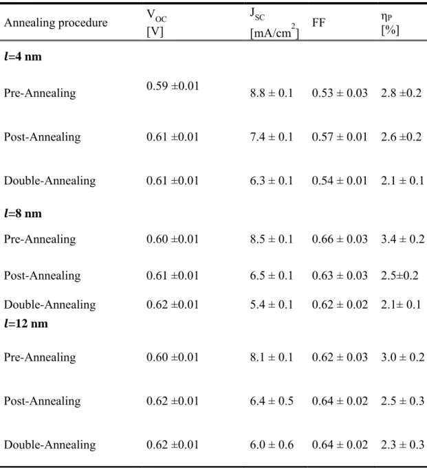
Three device sets are investigated to examine the impact of the annealing sequence and the MoOx layer thickness on the device performance. The current-voltage curves of pre-, post-
and double-annealed devices bearing a MoOx layer thickness (l) of 4, 8 and 12 nm are
displayed in Figure 2 and Figure S7a in Supplementary Information. The corresponding average device performance indicators (PCE, FF, VOC, ISC) and the corresponding standard
deviation derived from 16 solar cell devices are summarized in Table 1. The highest average PCE of 3.4 % is obtained for l= 8 nm and pre-annealing conditions. For l= 8 nm post- and doubleannealing procedures result in a lower average PCE of 2.5% and 2.1% (26.5% and -38.2% respectively). By analyzing the other performance indicators, the reduction of the PCE in post and double annealed devices appears to be mainly caused by the significant decrease of JSC (by -23.5% and - 36,5%, respectively) while other indicators are almost unaffected by
the thermal treatment sequence. Similar results are observed independently from the MoOx
layer thickness (for l=4 and l=12 nm). The JSC induced decay of the PCE was previously
reported for solar cells treated by a thermal aging procedure (ISOS-D2),26 and explained by (i) interface degradation mechanisms or by (ii) the diffusion of the top electrode material into the photoactive blend.27 Since both reasons can explain the decreased JSC observed for post- and
double-annealed devices, the morphology of the photoactive blend and the properties of the MoOx interfacial layer will be carefully investigated in the next section.
(a) (b)
Figure 2. J-V characteristic of investigated device sets subjected to the pre-, post- and
B. Composition and interface depth profile analyses
In contrast to the general consensus concerning Al diffusion at the P3HT:PCBM/Al interface, previous reports about the P3HT:PCBM/MoOx interface are much more controversial.
Namely, for ITO/MoO3/P3HT:PCBM/Al devices, MoOx was shown to diffuse through the
whole photoactive layer,23 while this behavior was not observed for Glass/ITO/TiOx/P3HT:PCBM/MoOx/Ag devices.24 To assess the potential diffusion of Mo
and/or MoOx related species in the devices fabricated following our three annealing
procedures, the chemical composition of the MoOx layer was investigated by XPS and
ToF-SIMS depth profiling. XPS profiles were made with low energy (500 eV) Ar+ sputtering and ToF-SIMS with low-energy Cs+ in order to limit sputtering induced artifacts and preserve the
device interfaces.28,29 The accurate peak fitting of Mo 3d core level spectra acquired at different sputtering times (i.e. depths) evidence a variable in-depth chemical composition of the MoOx layer with a more oxidized (~MoO3) state at the Ag/MoOx interface and a less
oxidized layer (~MoO) at the MoOx/P3HT:PCBM interface (Figure 3a and 3b). Interestingly,
the depth evolution of the MoOx layer chemical composition was almost identical for the
devices subjected to the pre- or double-annealing procedures (Figure 3c and 3d and Figure
S5). To improve the detection limit with respect to XPS analysis (~0.1 atomic %) and more
safely exclude that the depth-dependent MoOx layer composition variation is the result of the
preferential sputtering of oxygen species by the low-energy Ar+ beam.30,31
ToF-SIMS depth profiles were performed with low-energy Cs+ beam on pre- (Figure 4) or
double-annealed (Figure S6) devices. From the comparative analysis of MoO-, MoO2- and
MoO3- molecular signals profiles (note that each fragment is characterized by its specific
ionization yield) in pre- and double-annealed devices, we clearly observe perfectly similar features, i.e. (i) a negligible diffusion of MoOx across the P3HT:PCBM, (ii) the presence of
the three oxidation states in agreement with XPS results and (iii) that the thermal annealing procedure does not sensibly affect the MoOx layer composition. From this clear experimental
results we can safely assess that the performance differences in the solar cells exposed to different thermal annealing schemes are not ascribed to differences in the MoOx layer
composition or by interdiffusion effects at the P3HT:PCBM/MoOx interface.
The use of low energy sputtering beams allows limiting although not completely excluding preferential sputtering of oxygen (i.e. the reduction of MoOx species); however, the oxidation
profile is mainly ascribed to the high-vacuum thermal evaporation process of the MoO3
precursor, namely by the possibly different sticking coefficients of oxygen and Mo atoms on the BHJ surface.32
Figure 3. Fitting procedure of the XPS Mo 3d spectra acquired at different depths for a
double-annealed device. Different oxidation states of molybdenum are found at the upper (Ag/MoOx) interface (a) and at the lower (MoOx/P3HT:PCBM) interface (b). XPS depth
profiles with 500 eV Ar+ sputtering beam show very similar Mo layer chemical composition profiles in solar cells subjected to pre- (c) or double-annealing (d) procedures.
Figure 4. (a) ToF-SIMS depth profiles obtained on device fabricated following the
pre-annealing scheme. (b) Comparison between MoO-, MoO
2- and MoO3- molecular signals
derived from pre- or double-annealed devices.
C. Influence of the thermal annealing sequence on the bulk heterojunction morphology
The P3HT:PCBM BHJ morphology was characterized in devices bearing the same MoOx
layer thickness (l=8 nm) but treated by different thermal annealing procedures. AFM topography and phase images did not reveal any significant annealing procedure (see Figure
S1 and S3 in Supplementary Information). Moreover, the associated phase images do not
allow distinguishing between the individual components of the photoactive layer to eventually evidence phase separation within the photoactive layer (Figure S1). It was previously
reported that prolonging the annealing time resulted in the enhancement of the vertical segregation of the PCBM phase and possibly lead to the formation of µm-sized PCBM aggregates which considerably increased the charge recombination rate.33–38 In our case,
since PCBM aggregates are not observed at the BHJ surface, maybe because of the too short annealing time, we considered an alternative approach consisting of washing the BHJ film with dichloromethane (DCM) in order to dissolve PCBM without affecting the P3HT morphology. Therefore, we expected the appearance of cavities in the film morphology corresponding to PCBM-rich phases. To confirm the successful removal of the PCBM species from the P3HT:PCBM layer following the DCM treatment, we performed photoluminescence and absorbance investigations. Regardless of the thermal annealing procedure, the photoluminescence and the absorbance properties of DCM washed P3HT:PCBM layers are similar to those observed for a pristine P3HT layer (i.e. without PCBM, see Figure 5a and
5b). The suppression of the quenching effect from PCBM is a clear indication of the PCBM
removal by DCM. In addition, the absorbance spectrum of pristine P3HT layers does not change upon DCM treatment (shown in Figure S2 in Supplementary Information), confirming that the bulk of the P3HT is not affected by the solvent treatment, whereas the absorbance spectra of P3HT:PCBM layers differs significantly from pristine P3HT films. (see inset-graph in Figure 5b).
(a) (b)
Figure 5. (a) Fluorescence spectra from P3HT, P3HT:PCBM and DCM-treated
P3HT:PCBM layers subjected to the pre- or double-annealing procedure. (b) Absorbance spectra of DCM washed P3HT and P3HT:PCBM layers subjected to the pre- or double-annealing procedures. The inset-graph shows the absorbance spectra of thermally annealed P3HT and P3HT:PCBM layers before DCM treatment.
We further investigated by AFM the surface morphology of P3HT:PCBM films subjected to the different thermal annealing procedures and to the DCM treatment. The AFM images are taken both at open areas between the electrodes (see Figure 6a-c) and underneath the electrodes (see Supplementary Information Figure S4). For both regions and regardless of the applied thermal annealing procedure, the DCM treatment results in the appearance of cavities, whose density is significantly higher in post- and double- annealed devices. For these devices, we observe an almost uniform dense distribution of sub-micrometer scale cavities, while in pre-annealed devices, only few sparse micrometer scale cavities are observed (see Figure
6a-c). To investigate the origin of these cavities and to discriminate whether they can be
correlated to the removal of PCBM-rich phases, pristine P3HT films were also annealed and washed with DCM in a similar manner as the P3HT:PCBM layers. Surprisingly, and regardless of the thermal annealing procedure, the cavities in DCM washed P3HT are very
similar than the ones observed at P3HT:PCBM films (see Figure 6d-f). This leads us to the conclusion that the cavities appearing following DCM treatment originate from the partial removal of P3HT domains. Previous reports focusing on the solubility of P3HT in DCM evidenced that high-MW P3HT (as used within this study) is almost insoluble in DCM while
regio-random and low-MW P3HT impurities can be solubilized by DCM washing.39,40 In
summary, we observe a clear difference between the three differently annealed and DCM washed P3HT:PCBM samples. However, the occurrence of the DCM-induced cavities in P3HT:PCBM films cannot be exclusively related to the removal of PCBM as shown by the outcome of the control experiments where pristine P3HT layers were treated with DCM. To correlate the results obtained from our morphological investigation to the key performance indicators of solar cells, the behavior voltage dependent photocurrent in dependence of the applied thermal annealing procedure and the MoOx layer thickness is discussed in the
(a) P3HT:PCBM, Pre-Annealed (b) P3HT:PCBM, Post-Annealed (c) P3HT:PCBM, Double-Annealed (d) P3HT As-Cast (e) P3HT Pre-Annealed (f) P3HT Double-Annealed
Figure 6: AFM topography images of annealed P3HT:PCBM (a-c) and P3HT (d-f) films
exposed to DCM. Images (a), (b) and (c) are acquired in regions between the metal electrodes.
D. Impact of the thickness of the MoOx layer and the thermal treatment procedure on the charge extraction
Since neither the interface depth profiles nor the morphological characterization could give valuable information to derive structure-to-performance relationships in solar cells, we characterized the charge extraction regimes by the conventional approach of plotting photocurrent-effective voltage (Jph-Veff) curves in a double-logarithmic scale.
We firstly restrict our discussions on pre-annealed solar cells bearing different MoOx layer
thicknesses. The effects of the MoOx layer thickness on the overall device performance has
been extensively investigated by a number of different approaches, including fitting of the obtained JV curve to an equivalent electrical circuit model. In this case, for a MoOx layer
thicknesses < 3 nm the low device performance, caused by a decreased VOC, JSC and FF, was
ascribed to an increased series resistance and/or by a decreased shunt resistance.43,44 Investigating the effect of a varied MoOx layer thickness on the voltage dependent photocurrent shows for small Veff <0.1 V an ohmic transport regime (i.e. 𝐽𝑝ℎ ∝ 𝑉𝑒𝑓𝑓𝑘 with
k=1), while increasing Veff > 0.2 V leads to saturation of the photocurrent (k=0) as shown in
Figure 7. A similar trend of the photocurrent is observed for both 𝑙=8 nm and 𝑙=12 nm, whereas Jph is slightly lowered for devices bearing a higher MoOx layer thickness than 8 nm.
The shape of the extraction efficiency, which we define by normalizing the photocurrent Jph(Veff) to the photocurrent observed at Veff = 2.2V (see Eq. 3), is in good agreement with
results obtained from the Sokel-Hughes model showing a linear increase for small Veff and
saturation of Jph for high effective voltages. Thus, for pre-annealed devices with 𝑙≥8 nm
recombination and trapping mechanisms are apparently not affecting charge extraction. However, for 𝑙=4 nm, Jph(Veff) differs significantly within 0.2< Veff < 0.5 V and saturation of
the photocurrent is only observed when increasing Veff > 0.5 V. An exponent of k ~ 0.3 was
derived for 0.2 < Veff < 0.5 V, which does not allow for an association with space charge or
recombination limited transport regimes as this would require an exponent k=0.5 .25,41,42 The effective voltage Veff acting on charge carriers within a device can be understood in general as
the sum of the applied external voltage and the built-in voltage Vbi which depends on the
HOMO and LUMO level of the donor and acceptor material as well as on the work function of the electrode materials.51 In a previous report, investigating the development of the work function in relation to the film thickness for metal oxide layers, it was shown that the work function of metal oxides become stable only above a certain layer thickness; for MoOx a
critical thickness of 𝑙=5 nm was derived.46 Hence, for devices bearing a MoO
x layer thickness
below this critical value an energy level mismatch is observed between the HOMO energy level of P3HT and the MoOx work function. As a consequence, such devices require a larger effective voltage to reach saturation of the photocurrent while for small Veff the charge
extraction efficiency is affected by surface recombination due to the lower charge selectivity of the anode. 45
(a) (b)
Figure 7. (a) JPh-Veff curves obtained for the pre-annealed solar cell devices (with 𝑙=8 nm)
showing the derived photocurrent (JPh) and the compensation voltage (V0). (b) Comparison
between the JPh characteristics for pre-annealed solar cells differing by the respective MoOx
layer thickness (𝑙=4, 8 or 12 nm). The exponent k derived from the exponential relation Jph ~
Veff k, is indicated by dashed lines. For devices with a MoOx layer thickness > 8 nm the
voltage-dependent charge extraction efficiency shows a similar exponential relationship on the effective voltage as high-lighted at the inset graph in (b).
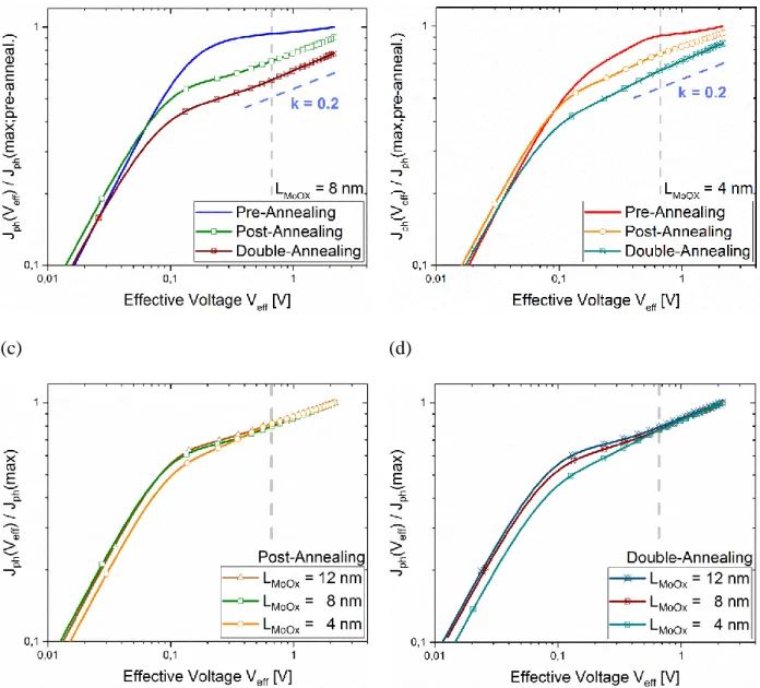
In the following, the voltage dependent charge extraction efficiency is discussed as a function of the thermal annealing procedure. The comparison between the voltage dependent charge extraction efficiency defined as the ratio of Jph(Veff) to Jph(max, Veff = 2.2) observed for
pre-annealed devices is given in Figure 8a and Figure 8b for devices with 𝑙= 4, 8 nm; for devices with 𝑙= 12 nm see Figure S7 in Supplementary Information. With respect to pre-annealed devices, post- and double-pre-annealed solar cells feature an overall lower photocurrent
for Veff > 0.1 V. Furthermore, the photocurrent does not saturate for Veff > 0.3 V, but rather
increases with a constant exponent k ~ 0.2. Hence, for post- and double annealed devices a higher internal field (i.e. Veff) is needed to sweep out light-generated charges and to reach the
saturation regime. Moreover, a similar behavior of the charge extraction efficiency for Veff >
0.6 V is observed independently of the MoOx layer thickness for post and double-annealed
devices, as shown in Figure 8c and Figure 8d.
The dependence of the derived light-generated photocurrent with respect to different magnitudes of the effective voltage has been investigated by Mihailetchi et. al,41 showing that for small effective voltages Jph can be described by the model proposed by Sokel and
Hughes,51 while for large V
eff the behavior of the photocurrent becomes governed by the
dissociation probability of the polaron pairs which was developed by Onsager and extended later by Braun.49,50 In a different approach based on fundamental statistics of fermions it was shown that non-geminate recombination dominate when V~VOC (i.e small Veff) while
geminate recombination dominates at low applied voltages (V~0 V, or Veff > 0.4 V), i.e at
high internal electric field.47 Hence, for the pre-annealed solar cell with l=4 nm, the extraction
of light-generated charges is mainly limited by non-geminate recombination of (free) charge carriers at the anode that can be suppressed by increasing the MoOx layer thickness. In
contrast, for post- and double-annealed devices the behavior of the photocurrent cannot be related to the MoOx thickness for Veff > 0.6 V and thus the charge extraction efficiency is
mainly limited by geminate recombination that can be only overcome by increasing the effective voltage. In the following section we will show how the individual performance indicators (VOC, FF and JSC) are affected by the different recombination mechanisms.
(c) (d)
Figure 8. Charge extraction efficiency of post- and double annealed solar cell devices
compared to pre-annealed devices with a MoOx layer thickness 𝑙=8 nm (a) and 𝑙=4 nm (b).
For post- and double-annealed devices the behavior of the charge extraction efficiency differs in dependence of the MoOx layer thickness for small Veff but becomes similar for Veff > 0.6 V
(c, d).Dashed lines correspond to the linear fit values used to evaluate the power law k (Jph ~
E. Influence of the MoOx layer thickness and the annealing procedure on the solar cell performance indicators
The results obtained from the JPh-Veff curves allow for a rigid interpretation of the evolution of
individual performance indicators with the MoOx layer thickness and the annealing procedure.
The optimum conditions giving the best performance (ηp = 3.4 ± 0.2 %, JSC = 8.5 ± 0.1
mA/cm2 and FF = 0.66 ± 0.3), correspond to pre-annealed devices with l=8 nm. This result is in good agreement with our observations of the voltage dependent charge extraction efficiency, which showed an ohmic behavior for Veff < 0.1 while becoming saturated for Veff
> 0.2 V. However, for devices with a lower MoOx layer thickness (l=4 nm), the JSC increases
by 3.5% but the FF decreases by -19.7 %, resulting in a significantly lowered PCE (-18%). Increasing the MoOx thickness (l=12 nm) results also in a drop of the FF (-6.1%) and to a reduction of JSC (-4.7%). The drop of FF is ascribed to the different behavior of the charge
extraction efficiency within 0.1 V < Veff < 0.3 V (see Figure 7b). This effective voltage
interval corresponds to an external voltage range of 0.6 V < Vext < 0.4V and thus to the
interval where FF is derived (see Eq. 1). Interestingly, we find JSC increased for l= 4 nm but
an opposite trend for devices with l >8 nm and which cannot be explained by the behavior of the voltage dependent charge extraction efficiency. In agreement with previous reports we attribute the different behavior of JSC in dependence of the MoOx thickness to different series
and shunt resistance of each respective device, where both resistors were acquired through fitting of the JV curve to an equivalent circuit model.23,26,43 The J
SC reduction observed for
post- and double-annealed solar cells and regardless of l, is a consequence of the Jph
suppression for Veff > 0.1 V which can be explained by geminate charge recombination due to
a significantly lowered polaron pair dissociation probability.
To sum up, our results indicate the necessity of accurately optimizing the MoOx layer
thickness and the annealing-procedure for maximizing the charge carrier extraction efficiency and reducing geminate and non-geminate charge recombination. Moreover, the final JSC and
the FF values are affected differently by varying the MoOx layer thickness or the annealing
procedure as indicated by the charge recombination mechanism occurring in different voltage intervals.
Table 1. Derived performance indicators of solar cells with different MoOx layer
thicknesses (𝑙) and thermal annealing procedures. Presented results are the average and the standard deviation derived from 16 cells for each individual case.
Annealing procedure VOC [V] JSC [mA/cm2] FF ηP [%] 𝒍=4 nm Pre-Annealing 0.59l±0.01 8.8 ± 0.1 0.53 ± 0.03 2.8 ±0.2 Post-Annealing 0.61 ±0.01 7.4 ± 0.1 0.57 ± 0.01 2.6 ±0.2 Double-Annealing 0.61 ±0.01 6.3 ± 0.1 0.54 ± 0.01 2.1 ± 0.1 𝒍=8 nm Pre-Annealing 0.60 ±0.01 8.5 ± 0.1 0.66 ± 0.03 3.4 ± 0.2 Post-Annealing 0.61 ±0.01 6.5 ± 0.1 0.63 ± 0.03 2.5±0.2 Double-Annealing 0.62 ±0.01 5.4 ± 0.1 0.62 ± 0.02 2.1± 0.1 𝒍=12 nm Pre-Annealing 0.60 ±0.01 8.1 ± 0.1 0.62 ± 0.03 3.0 ± 0.2 Post-Annealing 0.62 ±0.01 6.4 ± 0.5 0.64 ± 0.02 2.5 ± 0.3 Double-Annealing 0.62 ±0.01 6.0 ± 0.6 0.64 ± 0.02 2.3 ± 0.3
IV. Conclusion
The effect of the MoOx layer thickness and the thermal annealing procedure on the
performance and charge extraction efficiency has been investigated for the inverted ITO/PEI/P3HT:PCBM/MoOx/Ag solar cell structure. In addition, the photoactive layer
morphology was examined through an original approach combining DCM treatment and AFM analysis. Absorbance and photoluminescence measurements have proved the successful PCBM removal upon DCM treatment and AFM analysis has shown the formation of circular-shaped cavities which were ascribed to the partial dissolution of low-MW and regio-random
P3HT domains present at the BHJ surface. The in-depth chemical and molecular composition of the MoOx layer and its interfaces, characterized by XPS and ToF-SIMS, shows the
presence of a gradient Mo oxidation profile, with a more oxidized layer (~MoO3) at the
MoOx/Ag interface and a less oxidized state (~MoO) at the P3HT:PCBM/MoOx interface
possibly due to the different sticking coefficient of oxygen and molybdenum species. Interestingly, neither the MoOx oxidation profile nor the (weak) diffusion of the MoOx species
in P3HT:PCBM are influenced by the thermal annealing procedure. Log-log JPh-Veff curves
were analyzed to identify the different charge extraction regimes by the respective power law fit coefficient k (Jph ~ Veffk). For the best performing solar cells (pre-annealing and l=8 nm) an
ohmic regime (k=1) is observed at Veff~VOC followed by a saturation regime (k=0) at Veff >
0.3 V indicating an optimal carrier sweepout. The reduction of the MoOx layer thickness
introduces an intermediate charge extraction regime (k=0.28) at 0.2< Veff< 0.5 V. In post- or
double-annealed solar cells, a similar regime (with k~0.2) is observed for Veff > 0.4 V.
Intermediate charge extraction regimes occur in different effective voltage ranges, indicating for different charge recombination mechanisms and well-explain the JSC and FF reduction for
non-optimized process conditions. The results clearly indicate that exceeding a minimum MoOx layer thickness (~5 nm) and application of an optimized thermal annealing procedure
(here by the pre-annealing scheme) is mandatory to maximize the charge extraction efficiency and thus the overall solar cell performance.
Supporting Information
The supporting information provides additional experimental results, including AFM images for regions below the electrodes, absorbance spectra, XPS depth profiles, TOF-SIMS depth profiles and JV curves.
Acknowledgement
F.K. would like to acknowledge the financial support from FWF through the project PLASMOSOL (TRP-304-N20). Franz Peter Wenzl and Mirella El Gemayel are gratefully acknowledged by F.K. for fruitful discussions and proofreading the manuscript.
1 A. J. Moulé and K. Meerholz, “Morphology Control in Solution-Processed
Bulk-heterojunction Solar Cell Mixtures,” Adv. Funct. Mater. 19, 3028–3036 (2009).
2 Y. Huang, E. J. Kramer, A. J. Heeger and G. C. Bazan, “Bulk Heterojunction Solar Cells:
Morphology and Performance Relationships,” Chem. Rev. 114, 7006–7043 (2014).
3 B. Ray, P. R. Nair and M. A. Alam, “Unraveling the Role of Morphology on Organic Solar
Cell Performance,” vol. 47906,pp. 1–10.
4 R. Steim, F. R. Kogler and C.J. Brabec, “Interface Materials for Organic Solar Cells,” J.
Mater. Chem. 20, 2499 (2010).
5 H. Zeng, X. Zhu, Y. Liang and X. Guo, “ Interfacial Layer Engineering for Performance
6 W. H. Tseng, M. H. Chen, J. Y. Wang, C. T. Tseng, H. Lo, P. S. Wang, C. I. Wu,
“Investigations of Efficiency Improvements in Poly(3-Hexylthiophene) Based Organic
Solar cells Using Calcium Cathodes,” Sol. Energ. Mat. Sol. Cells 95, 3424–3427 (2011).
7 C. J. Brabec, S. E. Shaheen, C. Winder, N. S. Sariciftci and P. Denk, “Effect of LiF/Metal
Electrodes on the Performance of Plastic Solar Cells,” Appl. Phys. Lett. 80, 1288–1290 (2002).
8 S.-J. Lee, S. Jeong, D.-H. Kim, C. Kim and Y.-S. Han “Inverted Polymer Solar Cells with
an Ultrathin Lithium Fluoride Buffer Layer,” J. Nanosci. Nanotechnol. 12(4), 3205–3209 (2012).
9 Y. Udum, P. Denk, G. Adam, D.H. Apaydin, A. Nevosad, C. Teichert, M.S. White, N.S.
Sariciftci and M.C. Scharber, “Inverted Bulk-Heterojunction Solar Cell with Cross-Linked Hole-Blocking Layer,” Org. Electron. 15, 997–1001 (2014).
10 K. Sun, S. Zhang, P. Li, Y. Xia, X. Zhang, D. Du, F.H. Isikgor and J. Ouyang, “Review on
Application of PEDOTs and PEDOT:PSS in Energy Conversion and Storage Devices,” J. Mater. Sci.: Mater. Electron. 26, 4438–4462 (2015).
11 F. Ongul, S.A. Yuksel, M. Kazici, S. Bozar, A. Gunbatti and S. Gunes, “Effects of
Different Formulation PEDOT:PSS Hole Transport Layers on Photovoltaic Performance of Organic Solar Cells,” Polym.Adv.Technol. 28, 947–951 (2017).
12 C. Tao, S. Ruan, G. Xie, X. Kong, L. Shen, F. Meng, C. Liu, X. Zhang and W. Chen, “Role
13 D. Y. Kim, J. Subbiah, G. Sarasqueta, F. So, H. Ding, Irfan and Y. Gao, “The Effect of
Molybdenum Oxide Interlayer on Organic Photovoltaic Cells,” Appl. Phys. Lett. 95, 093304 (2009).
14 C. Tao, S. Ruan, X. Zhang, G. Xie, L. Shen, X. Kong, W. Dong, C. Liu and W. Chen,
“Performance Improvement of Inverted Polymer Solar Cells with Different Top Electrodes
by Introducing a MoO3 Buffer Layer,” Appl. Phys. Lett. 93, 2008–2010 (2008).
15 J. Y. Kim, S. H. Kim, H.H. Lee, K. Lee, W. Ma, X. Gong and A. J. Heeger, “New
Architecture for High-Efficiency Polymer Photovoltaic Cells Using Solution-Based Titanium Oxide as an Optical Spacer,” Adv. Mater. 18, 572–576 (2006).
16 Y. Zhang, A. K. Pandey, C. Tao, Y. Fang, H. Jin, P. L. Burn and P. Meredith, “Spectral
Response Tuning Using an Optical Spacer in Broad-Band Organic Solar Cells,” Appl. Phys. Lett. 102, 013302 (2013).
17 M. Campoy-Quiles, M. Schmidt, D. Nassyrov, O. Peña, A. R. Goñi, M. I. Alonso and M.
Garriga, “Real-Time Studies During Coating and Post-Deposition Annealing in Organic Semiconductors,” Thin Solid Films 519, 2678–2681 (2011).
18 A. J. Pearson, T. Wang, D. G. Lidzey, “The Role of Dynamic Measurements in Correlating
Structure with Optoelectronic Properties in Polymer : Fullerene Bulk-Heterojunction Solar Cells,” Rep. Prog. Phys. 76, 022501 (2013).
19 H. J. Kim, J. H. Park, H. H. Lee, D. R. Lee and J. J. Kim, “The Effect of Al Electrodes on
the Nanostructure of Poly(3-Hexylthiophene): Fullerene Solar Cell Blends During Thermal Annealing,” Org. Electron. 10, 1505–1510 (2009).
20 G. Li, V. Shrotriya, Y. Yao, Y. Yang, “Investigation of Annealing Effects and Film
Thickness Dependence of Polymer Solar Cells Based on Poly(3-Hexylthiophene),” J. Appl. Phys. 98, 043704 (2005).
21 N. Rujisamphan, F. Deng, R. E. Murray, C. Ni and S. Ismat Shah, “Focused Ion Beam
Assisted Investigations of Al Interface in Polythiophene:Fullerene Solar Cells,” Sol. Energy Mater Sol. Cells 109, 56–62 (2013).
22 F. Li, J. Zhao, K. Yao and Y. Chen, “Origin of the Efficiency Improvement in
Pre-Annealed P3HT/PCBM Solar Cells with LiF/Al Electrodes,” Chem. Phys. Lett. 553, 36–40 (2012).
23 M. Nyman, S. Dahlström, O. J. Sandberg and R. Österbacka, “Unintentional Bulk Doping
of Polymer-Fullerene Blends from a Thin Interfacial Layer of MoO3,” Adv. Energy Mater.
6, 1600670 (2016).
24 S. Chambon, L. Derue, M. Lahaye, B. Pavageau, L. Hirsch and G. Wantz, “MoO3
Thickness, Thermal Annealing and Solvent Annealing Effects on Inverted and Direct Polymer Photovoltaic Solar Cells,” Materials 5, 2521–2536 (2012).
25 A. M. Goodman and A. Rose “Double Extraction of Uniformly Generated Electron-Hole
Pairs from Insulators with Noninjecting Contacts,” J. Appl. Phys. 42, 2823(1971).
26 M. O. Reese, S. A. Gevorgyan, M. Jørgensen, E. Bundgaard, S. R. Kurtz, D. S. Ginley, D.
C. Olson, M. T. Lloyd, P. Morvillo, E. A. Katz, A. Elschner, O. Haillant, T. R. Currier, … F. C. Krebs, “Consensus Stability Testing Protocols for Organic Photovoltaic Materials and Devices,” Sol. Energy Mater Sol. Cells 95, 1253–1267 (2010).
27 W. Greenbank, L. Hirsch, G. Wantz and S. Chambon, “Interfacial Thermal Degradation in
Inverted Organic Solar Cells,” Appl. Phys. Lett. 107, 263301 (2015).
28 Y. Busby, E. J. W. List-Kratochvil and J.-J. Pireaux, “Chemical Analysis of the Interface in
Bulk-Heterojunction Solar Cells by X-ray Photoelectron Spectroscopy Depth Profiling,” ACS Appl. Mater. Interfaces 9, 3842–3848 (2017).
29 F. Matteocci, Y. Busby, J.-J. Pireaux, G. Divitini, S. Cacovich, C. Ducati and A. Di Carlo,
“Interface and Composition Analysis on Perovskite Solar Cells,” ACS Appl. Mater.
Interfaces 7, 26176–26183 (2015).
30 X. Li, K. A. Wepasnick, X. Tang, Y. Wang, K. H. Bowen, D. H. Fairbrother and G.
Gantefoer, “Ion Induced Modification of Size-Selected MoO3 and WO3 Clusters Deposited on HOPG,” J. Vac. Sci. Technol. B 30, 31806 (2012).
31 H. Simchi, B. E. McCandless, T. Meng and W. N. Shafarman, “Structure and Interface
Chemistry of MoO3 Back Contacts in Cu(In,Ga)Se 2 Thin Film Solar Cells,” J. Appl. Phys. 115, 033514 (2014).
32 G. Nagy and A. V. Walker, “Dynamics of Reactive Metal Adsorption on Organic Thin
Films,” J. Phys. Chem. C 111, 8543–8556 (2007).
33 L. Chang, H. W. A. Lademann, J. B. Bonekamp, K. Meerholz, and A. J. Moulé, “Effect of
Trace Solvent on the Morphology of P3HT:PCBM Bulk Heterojunction Solar Cells”. Adv. Funct. Mater. 21, 1779–1787 (2011).
34 W. C. Tsoi, S. J. Spencer, L. Yang, A. M. Ballantyne, P. G. Nicholson, A. Turnbull, A. G.
the Electronic Energy Levels and Thin Film Morphology of P3HT: PCBM Blends,” Macromolecules 44, 2944–2952 (2011).
35 B. Kadem, A. Hassan, and W. Cranton, “Efficient P3HT:PCBM Bulk Heterojunction
Organic Solar cells; Effect of Post Deposition Thermal Treatment,” J. Mater. Sci.: Mater. Electron 27, 7038–7048 (2016).
36 W. Wang, S. Guo, E. M. Herzig, K. Sarkar, M. Schindler, D. Magerl, M. Philipp, J. Perlich
and P. Müller-Buschbaum, “Investigation of Morphological Degradation of P3HT:PCBM Bulk Heterojunction Films Exposed to Long-Term Host Solvent Vapor,” J. Mater. Chem. A 4, 3743–3753 (2016).
37 S. A. Dowland, M. Salvador, J. D. Perea, N. Gasparini, S. Langner, S. Rajoelson, H. H.
Ramanitra, B. D. Lindner, A. Osvet, C. J. Brabec, R. C. Hiorns and H. J. Egelhaaf, “Suppression of Thermally Induced Fullerene Aggregation in Polyfullerene-Based
Multiacceptor Organic Solar Cells,” ACS Appl. Mater. Interfaces 9, 10971–10982 (2017).
38 H. H. Ramanitra, S. A. Dowland, B. A. Bregadiolli, M. Salvador, H. Santos Silva, D.
Bégué, C. F. O. Graeff, H. Peisert, T. Chassé, S. Rajoeleson, A. Osvet, C. J. Brabec, H. J. Egelhaaf, … R. C. Hiorns, “Increased Thermal Stabilization of Polymer Photovoltaic Cells with Oligomeric PCBM,” J. Mater. Chem. C 4, 8121–8129 (2016).
39 A. L. Ayzner, C. J. Tassone, S. H. Tolbert and B. J. Schwartz, “Reappraising the Need for
Bulk Heterojunctions in Polymer - Fullerene Photovoltaics : The Role of Carrier Transport in All-Solution-Processed P3HT / PCBM Bilayer Solar Cells,” J. Phys. Chem. C 113, 20050–20060 (2009).
40 J. H. Park, J. S. Kim, J. H. Lee, W. H. Lee and K. Cho, “Effect of Annealing Solvent
Solubility on the Performance of Poly(3-Hexylthiophene)/Methanofullerene Solar Cells,” J. Phys. Chem. C 113, 17579–17584 (2009).
41 V. D. Mihailetchi, L. J. A. Koster, J. C. Hummelen and P. W. Blom, “Photocurrent
Generation in Polymer-Fullerene Bulk Heterojunctions,” Phys. Rev. Lett. 93, 19–22 (2004).
42 H. Azimi, A. Senes, M. C. Scharber, K. Hingerl and C. J. Brabec, “Charge Transport and
Recombination in Low-Bandgap Bulk Heterojunction Solar Cell Using Bis-Adduct Fullerene,” Adv. Energy Mater. 1, 1162–1168 (2011).
43 S. Noh, C. K. Suman, D. Lee, S. Kim and C. Lee, “Study of Buffer Layer Thickness on
Bulk Heterojunction Solar Cell,” J. Nanosci. Nanotechnol. 10, 6815–6818 (2010).
44 T. Stubhan, T. Ameri, M. Salinas, J. Krantz, F. MacHui, M. Halik and C. J. Brabec, “High
Shunt Resistance in Polymer Solar Cells Comprising a MoO3 Hole Extraction Layer Processed from Nanoparticle Suspension,” Appl. Phys. Lett. 98, 253308 (2011).
45 J. Reinhardt, M. Grein, C. Bühler, M. Schubert and U. Würfel, “Identifying the Impact of
Surface Recombination at Electrodes in Organic Solar Cells by means of Electroluminescence and Modeling,” Adv. Energy Mater. 4, 1400081 (2014).
46 M. T. Greiner, L. Chai, M. G. Helander, W. M. Tang and Z. H. Lu, “Metal/Metal-Oxide
Interfaces: How Metal Contacts Affect the Work Function and Band Structure of MoO3,” Adv. Funct. Mater. 23, 215–226 (2013).
47 S. R. Cowan, A. Roy and A. J. Heeger, “Recombination in Polymer-Fullerene Bulk
Heterojunction Solar Cells,” Phys. Rev. B 82, 245207 (2010).
48 M. Limpinsel, A. Wagenpfahl, M. Mingebach, and C. Deibel, “Photocurrent in Bulk
Heterojunction Solar Cells,” Phys. Rev B 81, 085203 (2010).
49 L. Onsager, “Deviations from Ohm's Law in Weak Electrolytes,” J. Phys. Chem. 2, 599
(1934).
50 C. L. Braun, “Electric Field Assisted Dissociation of Charge Transfer States as a
Mechanism of Photocarrier Production,” J. Phys. Chem. 80, 4157 (1984).
51 R. Sokel and R. C. Hughes, “Numerical analysis of transient photoconductivity in
insulators,” J. Appl. Phys. 53, 7412 (1984).
52 E. Siebert-Henze, V. G. Lyssenko, J. Fischer, M. Tietze, R. Brueckner, M. Schwarze, K.
Vandewal, D. Ray, M. Riede and K. Leo, “Built-in Voltage of Organic Bulk Heterojuction p-i-n Solar Cells measured by Electroabsorption Spectroscopy” AIP Adv. 4, 047134 (2014).