HAL Id: hal-01745729
https://hal.archives-ouvertes.fr/hal-01745729
Submitted on 28 Mar 2018HAL is a multi-disciplinary open access
archive for the deposit and dissemination of sci-entific research documents, whether they are pub-lished or not. The documents may come from teaching and research institutions in France or abroad, or from public or private research centers.
L’archive ouverte pluridisciplinaire HAL, est destinée au dépôt et à la diffusion de documents scientifiques de niveau recherche, publiés ou non, émanant des établissements d’enseignement et de recherche français ou étrangers, des laboratoires publics ou privés.
A Built-In Self-Test Structure (BIST) for Resistive
RAMs Characterization: Application to Bipolar
OxRRAMs
Hassen Aziza, Marc Bocquet, Mathieu Moreau, Jean-Michel Portal
To cite this version:
Hassen Aziza, Marc Bocquet, Mathieu Moreau, Jean-Michel Portal. A Built-In Self-Test Structure (BIST) for Resistive RAMs Characterization: Application to Bipolar OxRRAMs. International Semi-conductor Device Research Symposium, Dec 2013, Bethesda, United States. �hal-01745729�
ISDRS 2013, December 11-13. 2013
Built-In Self-Test Structure (BIST) for Resistive RAMs Characterization:
Application to Bipolar OxRRAMs
Hassen AZIZA, Marc BOQUET, Mathieu MOREAU and J-Michel PORTAL
IM2NP-UMR CNRS 6242, Aix-Marseille University, France, [email protected]
Problem Formulation: Resistive Random Access Memory (ReRAM) is a form of nonvolatile storage that operates by changing the resistance of a specially formulated solid dielectric material [1]. Among ReRAMs, Oxide-based Resistive RAMs (so-called OxRRAM) are promising candidates due their compatibility with CMOS processes and high ON/OFF resistance ratio. Common problems with OxRRAM are related to high variability in operating conditions and low yield. OxRRAM variability mainly impact ON/OFF resistance ratio. This ratio is a key parameter to determine the overall performance of an OxRRAM memory. In this context, the presented built-in structure allows collecting statistical data related to the OxRRAM memory array (ON/OFF resistance distributions) for reliability assessment of the technology.
Built-In Self-Test (BIST) structure: Fig. 1a presents the elementary array used for simulation which is constituted by a 3×3 1T/1R cell matrix, a row decoder, a column decoder and a sense amplifier for the read operation. The OxRRAM compact model used to build the memory array satisfactorily matches quasi-static and dynamic experimental data measured on actual HfO2-based devices (Fig. 1b). Notice that
the OxRRAM model allows a variability analysis based on OxRRAM card model parameters variation. The card model parameter variations are chosen to feet experimental data [2].
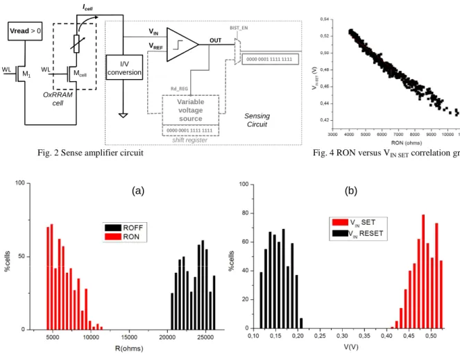
Fig. 2 presents the single-ended sense amplifier (solid line). The circuit working principle is quite simple. During a READ operation, the OxRRAM cell is biased throw the row decoder (with Vread > 0 and WL
high). The current cell value Icell is generated according to the memory state (RON≈7kΩ after a SET
operation and ROFF≈25 kΩ after a RESET operation). The comparator input VIN is directly proportional
to Icell and therefore to the OxRRAM resistance (two distinct values are available for VIN: VIN SET for RON
and VIN RESET for ROFF).
So that the sense amplifier operates properly, on the one hand the difference between VIN SET and VIN RESET
must be the highest and on the other hand VREF has to be set exactly between VIN SET and VIN RESET values.
At a circuit level, VIN is the parameter to consider in terms of memory functionality. To extract VIN value,
a variable voltage reference source and a multiplexer are incorporated in the sensing circuit (dotted part of the circuit) and the READ operation is modified as follow:
• VREF increases step by step from 0 to Vdd (VREF increase is controlled by a shift register),
• VIN value is detected when the sense amplifier output switches (the shifting process stops when
VREF > VIN, i.e Rd_REG signal becomes active),
• VIN is available at the circuit output in a numerical value when BIST_EN signal is high.
Simulation results:
To validate the BIST structure, a variability analysis is conducted through 500 Monte Carlo simulations. The elementary matrix presented in Fig. 1, embedding the BIST structure, is considered for simulations. As a result of cell variability, circuit performance exhibits much wider variability. In Fig. 3a, RON and ROFF distributions are plotted (RON/ROFF variability being correlated with actual silicon results). In Fig. 3b, VIN SET and VIN RESET distributions are also plotted. These last distributions are similar to RON and
ROFF distributions. This trend is confirmed by the correlation curve presented in Fig. 4. Therefore, the modified sense amplifier structure can be used as a powerful tool to track any resistance variations but also to characterize the memory array variability.
To summarize, a built in self-test structure is presented for Resistive RAM characterization and variability evaluation. The area overhead introduced by structure is relatively low as the structure is integrated in the sense amplifiers. The normal mode of operation of the memory is preserved. Besides, extracted values are given in a digital data format, so the extraction process does not required any analog pin on the tester, making it fully digital tester compliant or easily observable via the random logic.
ISDRS 2013, December 11-13. 2013 M00 M01 M02 M10 M11 M12 M20 M21 M22 Column Decoder Sense Amplifier OUT 0 OUT 1 OUT 2 R o w D e co d e r BL 0 BL 1 BL 2 WL 0 WL 1 WL 2 OxRRAM cell -1.5 -1.0 -0.5 0.0 0.5 1.0 10-9 10-8 10-7 10-6 10-5 10-4 10-3 0.0 0.5 1.0 10-9 10-7 10-5 10-3 10-1 101 103 105 Simu. Data [9] Set Reset (a) I C e ll ( A ) VCell (V) (b) T S e t VApp Simu. Data [9] (b) (a) (s ) (V)
Fig. 1 (a) OxRRAM memory array (a) I-V characteristic measured on HfO2-based devices and corresponding simulation using the OxRRAM model & SET voltage as a function of the programming ramp
I/V conversion OxRRAM cell Variable voltage source WL VIN Vread > 0 Sensing Circuit WL OUT Icell Mcell M1 0000 0001 1111 1111 VREF BIST_EN shift register 0000 0001 1111 1111 Rd_REG
Fig. 2 Sense amplifier circuit Fig. 4 RON versus VIN SET correlation graph
(b) (a)
Fig. 3 RON and ROFF distributions & VIN SET and VIN RESET distributions versus cell variability
References
[1] J. F. Gibbons & al, “Switching properties of thin Nio films”, Solid-State Electronics, vol. 7, issue 11, pp. 785-790. (1964).
[2] H. Aziza & al, “Evaluation of OxRAM cell variability impact on memory performances through electrical simulations”, Non-Volatile Memory Technology Symposium. (2011).