HAL Id: hal-01745759
https://hal.archives-ouvertes.fr/hal-01745759
Submitted on 16 Jul 2018
HAL is a multi-disciplinary open access
archive for the deposit and dissemination of
sci-entific research documents, whether they are
pub-lished or not. The documents may come from
teaching and research institutions in France or
abroad, or from public or private research centers.
L’archive ouverte pluridisciplinaire HAL, est
destinée au dépôt et à la diffusion de documents
scientifiques de niveau recherche, publiés ou non,
émanant des établissements d’enseignement et de
recherche français ou étrangers, des laboratoires
publics ou privés.
Analytical study of complementary memristive
synchronous logic gates
Jean-Michel Portal, Mathieu Moreau, Marc Bocquet, Hassen Aziza, Damien
Deleruyelle, Christophe Muller, Yue Zhang, Erya Deng, Jacques-Olivier Klein,
Damien Querlioz, et al.
To cite this version:
Jean-Michel Portal, Mathieu Moreau, Marc Bocquet, Hassen Aziza, Damien Deleruyelle, et al..
An-alytical study of complementary memristive synchronous logic gates.
2013 IEEE/ACM
Interna-tional Symposium on Nanoscale Architectures (NANOARCH), Jul 2013, Brooklyn, United States.
�10.1109/NanoArch.2013.6623047�. �hal-01745759�
Analytical Study of Complementary Memristive
Synchronous Logic Gates
J.M. Portal*, M. Moreau, M. Bocquet, H. Aziza,
D.Deleruyelle, C. Muller
IM2NP, Aix-Marseille Univ., UMR CNRS 7334 Marseille, France
Y. Zhang, E. Deng, J.O Klein, D. Querlioz, D.
Ravelosona, C. Chappert, W.S. Zhao**
IEF, Paris-Sud Univ., UMR CNRS 8622, Orsay, France
Abstract—This paper describes an analytical study of
synchronous logic gate design based on hybrid structure with MOS and resistive switching non-volatile memories (RS-NVMs). This type of structure allows ultra-low power consumption during power down, while often-used data are saved in RS-NVM cells. The parallel data sensing achieves low-power and fast computation time. The logic gate construction theory, from Boolean equation to hybrid MOS/RS-NVM tree, is deeply detailed. Read and write design guideline, regarding RS-NVM and MOS resistance balance are investigated. Practical implementation is given through transient simulations based on two memory technologies: STT-MRAM and OxRRAM to validate the concept by using CMOS 40 nm design kit and memory compact models.
Keywords—Low-Power design; synchronous logic gate; Resistive Switching; complementary cell;
I. INTRODUCTION
According to ITRS 2011, static power in modern computing systems, due to the high leakage currents, will start to play the major role of whole power consumption in the next years [1]. In order to relieve this power issue, emerging hybrid circuits based on resistive switching (RS) coupled with CMOS are under intense R&D investigation by both academics and industries. Spin transfer torque magnetic random access memory (STT-MRAM) [2] and Oxide Resistive RAM (OxRRAM) [3] are among the most encouraging technologies. They promise to provide high performances in terms of write/read speed, power, CMOS compatibility and endurance.
Even though these emerging RS memory technologies are based on different physics, they hold many common features. For instance, they are two terminal nanoscale devices; their resistances vary to present two ‘0’ and ‘1’ states; their memory cells are implemented at back-end of line (BEOL) process [4-5]. In this context, RS non-volatile logic gate (RS-NVLG) based on hybrid technology [6] could open the way towards ultra-low power high density ICs [7]. Moreover, RS-NVLG could also overcome the bottleneck of data communication between separated logic module and memory block. Recently, a number of innovative circuits based on hybrid RS memory/CMOS circuits have been developed. For example, magnetic look-up-table (MLUT) [8], Non Volatile flip-flop (NVFF) [9] and Non Volatile Full Adder (NVFA) [10] were introduced for reconfigurable logic circuits and power down applications. These circuits show encouraging performances
and particularly, a fully NVFA based on racetrack memory has been proposed [11].
This paper firstly presents a general analytical study to build hybrid MOS/RS non-volatile memories (RS-NVMs) logic gate from Boolean equations. We discuss the resistance configuration effect and their impact on read phase in synchronized hybrid logic gate. The impact of the resistance ratio between MOS and RS-NVMs is also discussed during the programming phase of the RS elements. Finally, demonstration of the concept on fundamental logic gates is given with two memory technologies: STT-MRAM and OxRRAM by using CMOS 40 nm design kit (DK) [12] and our NVM compact models [13-14].
The rest of the paper is organized as follows: in the next section, we introduce a general concept of hybrid MOS/RS memory synchronized logic gates, combining on one side PCSA and on the other side hybrid MOS logic tree with write circuitry to program RS cells. Resistance ratio and their impacts on read and programming phases are discussed in Section III and IV. Together with the RS cell compact models, Section V is dedicated to transient simulation results of fundamental logic gate to demonstrate the concept. Finally, a discussion and concluding remarks are provided in Section VI.
II. HYBRID LOGIC GATE GENERAL ARCHITECTURE
In this section, we introduce the general concept of synchronous hybrid logic gates based on the “logic-in-memory” principle mentioned in [7] with STT-MRAM. It allows a novel combination between logic unit and memory cell beyond Von-Neumann architecture. The distance of data movement becomes much shorter which promises lower power and faster speed. This principle is extended, here, from a theoretical point of view to basic logic gate combined with general RS-NVMs.
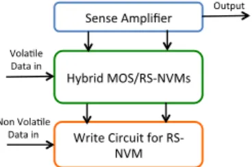
Fig. 1. Synchronous hybrid logic gate structure composed of sense amplifier, MOS/RS-NVMs tree and writing circuit.
Sense%Amplifier% Hybrid%MOS/RS5NVMs% Write%Circuit%for%RS5 NVM% Output% Vola@le% Data%in% Non%Vola@le% Data%in%
Synchronous hybrid logic gate structure is composed of three main blocks, as illustrated in Fig.1: a sense amplifier to set the gate outputs, an hybrid MOS/RS-NVMs tree to implement the logic function and a writing circuit to store non-volatile data in the RS-NVM elements. Sense amplifier and write circuit are used to interface the gate to the surrounding logic while the logic function is build with the hybrid MOS/RS-NVMs. Here we first focus on the description of the interface elements (sense amplifier and write circuit).
A. Sense Amplifier
In a low-power design context, the choice of the sense amplifier is mainly driven by the following constraints: low-power consumption, fast sensing time and robustness versus variation. Thereby, we use here a Pre-Charge Sense Amplifier (PCSA) [15], which showed high performance in terms of reliability, power and speed.
(a) (b)
Fig. 2. (a) Schematic of the pre-charge sense amplifier (PCSA). (b) Schematic of the basic write circuit.
As shown in Fig. 2(a), a PCSA consists of a pre-charge sub-circuit (MP2 and MP3), a discharge sub-circuit (MN2) and a pair of inverters (MN0-1 and MP0-1), which act as an amplifier. It operates in two phases: Pre-Charge phase and evaluation phase. During the first phase, the signal CLK is pulled down and the outputs (Qm and Qm ) are pulled up to
VDD or logic ‘1’ through MP2-3 while MN2 remains off.
During the second phase, CLK is pulled up, MP2-3 are turned off and MN2 on. As shown in Fig.2(a), the two hybrid
MOS/RS-NVMs branches F and F are in complementary
states, thus discharge currents are different in the two branches. The lower resistance branch is pulled down to reach the threshold voltage of transistor (MP1 or MP2) more quickly, at
the same time, the other branch will be pulled up to VDD or
logic ‘1’ and this low-resistance branch will continue to drop to
Gnd or logic ‘0’, setting the outputs of the PCSA. B. Write Circuit
The write circuit is basically composed of pass-transistors, as illustrated in Fig. 2(b), which connects respectively the top electrode (TE) and the bottom electrode (BE) of the RS-NVM elements. It is important to note that Input1 and Input2 should never be activated at the same time. In this case, to set the
RS-NVM element to a low resistive state (RLRS), Input1 has to be
pulled down, then TE is pulled up to Vdda and BE is grounded. Respectively, to reset the RS-NVM element to a high resistive
state (RHRS), Input2 has to be pulled up, then TE is grounded
and BE is pulled up to Vdda.
C. Hybrid MOS/RS-NVMs Tree
In a general manner, the logic function F to be implemented is a Boolean function of:
- Volatile data or variables that drive gates of MOS transistors,
- Non-volatile data or variables that are stored in RS-NVMs through a write process.
The read process is differential, thus the hybrid logic tree is designed with two branches, one implementing the function F
connected to output Qm and the other implementing the
function F connected to output Qm. It is important to note that the enable signal for the read process is logic ‘0’, thus we use complemented function to have a direct link between branches organization and Boolean equation. Considering two input basic gates (NAND, AND, NOR and OR), and knowing that synchronous hybrid logic gates present output Qm and
complementary output Qm, we can implement “AND and
NAND” and “OR and NOR” respectively using two single gates AND and OR respectively. So, to find the branches organization we only may focus on AND and OR Boolean equations as presented in Table I.
TABLE I. BOOLEAN EQUATIONS OF AND/ORGATE
Gate Qm Qm AND A.B A + B A ⋅ B + A ⋅ B + A ⋅ B B + A ⋅ B A ⋅ B + A OR A+B A ⋅ B A ⋅ B + A ⋅ B + A ⋅ B B + A ⋅ B A + A ⋅ B
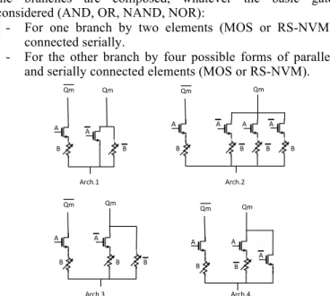
From Table I, considering that one variable is a volatile data and the other is a non-volatile data, it clearly appears that the branches are composed, whatever the basic gate considered (AND, OR, NAND, NOR):
- For one branch by two elements (MOS or RS-NVM) connected serially.
- For the other branch by four possible forms of parallel and serially connected elements (MOS or RS-NVM).
Fig. 3. Schematic of the four possible AND gate architectures (Arch.1 to Arch. 4). CLK $ CLK $ MP2 MP0 MP1 MP3 MN0 MN1 Qm$ Qm$ VDD$ RS2NVM0 $ CLK $ Gnd $ MN2 RS2NVM1 $ F" F" MP0 $ MP2 $ MN0 $ MN2 $ B$ B$ Input1 $ Input2 $ Input1 $ Input2 $ Gnd $ Gnd $ MP1 $ MN1 $ Input1 $ Input2 $ Gnd $ Vdda $ Vdda $ TE# BE# RS'NVM# A" B" B" A" Qm" Qm" B" A" Qm" B" A" B" A" A" B" Qm" Qm" B" B" A" B" Qm" A" Qm" A" B" Qm" B" A" Arch.1" Arch.2" Arch.3" Arch.4" A"
From this observation, Fig.3 shows all the possible architectures of a hybrid AND logic tree with A, a volatile data and B, a non-volatile data.
From a theoretical point of view, any synchronous hybrid logic basic gate can be designed by using one of the four architectures defined in the case of AND gate (see Fig.3) to build the hybrid logic tree.
III. ARCHITECTURE SIMPLIFICATION CONSIDERING
RESISTANCE RATIO
From a design point of view, the four architectures (Arch.1 to Arch.4), derived from Boolean equations (Table I), present different characteristics when considering resistance ratios between both branches and between MOS and RS-NVM elements. In this section, the resistance configurations of all the architectures are studied to propose design simplification. For this study, the transistor resistances for the advanced MOS
technology are estimated to RON=~10 kΩ and ROFF=~10 GΩ
according to [12]. Even RS-NVMs hold common behavioral features, their resistive characteristics are quite different and it is important to develop design strategies to manage these
differences. For STT-MRAM, its low resistance (RLRS) is some
kΩ and the TMR ratio is lower than 250% [16], which limits
the high resistance (RHRS) up to ~20 kΩ [17]. For OxRRAM,
its RLRS can be larger than 20 kΩ and its RHRS/RLRS ratio
achieves up a high value [18-20]. Regarding these values, it
confirms that ROFF of MOSFET is much larger than RHRS.
The Table II, III, IV and V summarize the resistance condition of respectively Arch.1, Arch.2, Arch.3 and Arch.4.
In these tables, A=‘1’ corresponds to RON, A=‘0’ to ROFF,
B=‘1’ to RLRS and B=‘0’ to RHRS. RL is the whole resistance of
the left branch connected to Qm and RR is the whole resistance
of the right branch connected to Qm. According to the
explanation in part II.C, when RL>RR output Qm is pulled
down to ’0’, and when RL<RR output Qm is pulled up to ’1’.
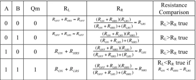
TABLE II. TRUTH TABLE AND RESISTANCE CONDITIONS OF ARCH.1
A B Qm RL RR Comparison Resistance 0 0 0 ROFF+ RHRS≈ ROFF RLRSRON RLRS+ RON RL>RR true 0 1 0 ROFF+ RLRS≈ ROFF RHRSRON RHRS+ RON RL>RR true 1 0 0 RON+RHRS RLRSROFF RLRS+ ROFF ≈ RLRS RL>RR true 1 1 1 RON+RLRS RHRSROFF RHRS+ ROFF ≈ RHRS RL<RR true if RON< RHRS− RLRS From the analysis of Table II, two observations can be established:
- The transistor on the right branch has no contribution on
the output. Indeed, when A=‘0’ ROFF of the left branch
ensures the correctness of the result, and, when A=‘1’ the RS-NVM resistance is dominant in the right branch. - The output Qm is properly set to ‘1’ only if the following
condition is respected RON< RHRS− RLRS.
Regarding the structure Arch.2, some remarks can be
drawn for the right branch resistance RR. Indeed, whatever the
value of A, the right branch presents OFF transistor(s) in parallel with ON transistor(s), thus we can only consider sub-branch(es) with ON transistor(s) in the Table III.
TABLE III. TRUTH TABLE AND RESISTANCE CONDITIONS OF ARCH.2
A B Qm RL RR approximation Comparison Resistance
0 0 0 ROFF+ RHRS≈ ROFF (RON+ RHRS)(RON+ RLRS) (RON+ RHRS) + (RON+ RLRS) RL>RR true 0 1 0 ROFF+ RLRS≈ ROFF (RON+ RHRS)(RON+ RLRS) (RON+ RHRS) + (RON+ RLRS) RL>RR true 1 0 0 RON+RHRS RON+ RLRS RL>RR true 1 1 1 RON+RLRS RON+ RHRS RL<RR true
From the analysis of Table III, two observations can also be established regarding the right branch:
- The two sub-branch activated with
A
have nocontribution on the outputs. Indeed, when A=‘0’ ROFF of
the left branch ensures the correctness of the result, and, when A=‘1’ the transistors of these two sub-branches are off while the sub-branch in parallel presents an ON transistor with a dominant effect.
- With A=’1’, the comparisons are both performed between branches presenting a MOS serially connected to a RS-NVM element, and no specific condition on resistance value is thus needed.
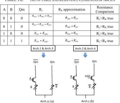
TABLE IV. TRUTH TABLE AND RESISTANCE CONDITIONS OF ARCH.3
A B Qm RL RR Comparison Resistance 0 0 0 ROFF+ RHRS≈ ROFF (RON+ RHRS)(RLRS) (RON+ RHRS) + (RLRS) ≈ RLRS RL>RR true 0 1 0 ROFF+ RLRS≈ ROFF (RON+ RLRS)(RHRS) (RON+ RLRS) + (RHRS) RL>RR true 1 0 0 RON+RHRS (ROFF+ RHRS)(RLRS) (ROFF+ RHRS) + (RLRS) ≈ RLRS RL>RR true 1 1 1 RON+RLRS (ROFF+ RLRS)(RHRS) (ROFF+ RLRS) + (RHRS) ≈ RHRS RL<RR true if RON< RHRS− RLRS
From the analysis, of Table IV, two observations can be founded regarding the right branch:
- The sub-branch composed of the transistor serially connected to the RS-NVM element has no contribution
on the outputs. Indeed, when A=‘0’ ROFF of the left
branch guarantees the correctness of the result, and, when A=‘1’ the RS-NVM resistance is dominant in the right branch.
- The output Qm is properly set to ‘1’ only if the following
condition RON< RHRS− RLRS is respected.
TABLE V. TRUTH TABLE AND RESISTANCE CONDITIONS OF ARCH.4
A B Qm RL RR Comparison Resistance
0 0 0 ROFF+ RHRS≈ ROFF (ROFF+ RLRS)(RON)
(ROFF+ RLRS) + (RON)
≈ RON RL>RR true
0 1 0 ROFF+ RLRS≈ ROFF (ROFF+ RHRS)(RON)
(ROFF+ RHRS) + (RON) ≈ RON RL>RR true 1 0 0 RON+RHRS (RON+ RLRS)(ROFF) (RON+ RLRS) + (ROFF) ≈ RON+ RLRS RL>RR true 1 1 1 RON+RLRS (RON+ RHRS)(ROFF) (RON+ RHRS) + (ROFF) ≈ RON+ RHRS RL<RR true
Finally, from the analysis, of Table V, two observations can be founded regarding the right branch:
- The sub-branch activated with A has no contribution on
the outputs. Indeed, when A=‘0’ ROFF of the left branch
ensure the correctness of the result, and, when A=‘1’ the transistor is off while the sub-branch in parallel presenting an ON transistor with a dominant effect. - With A=‘1’, the comparisons are both performed
between branches presenting a MOS serially connected to a RS-NVMs element, and no specific condition on resistance value is thus needed.
If we summarize the observations obtained on the four architectures:
- The structures Arch.1 and Arch.3 are equivalent in terms of resistance conditions, and work properly under the
condition RON< RHRS− RLRS, hence these both architectures
can be simplified to give a single optimized architecture (Architecture simplified with condition – Arch.sc) illustrated in Fig. 4(a).
- The structures Arch.2 and Arch.4 are equivalent in terms of resistance conditions, and work properly without specific conditions on resistance value, hence these both architectures can be simplified to give a single optimized architecture (Architecture simplified without condition – Arch.s) illustrated in Fig. 4(b).
The Table VI and VII respectively validate the efficiency of the simplified structure, which successfully compute the AND Boolean equation.
TABLE VI. TRUTH TABLE AND RESISTANCE CONDITIONS OF ARCH.SC
A B Qm RL RR approximation Comparison Resistance
0 0 0 ROFF+ RHRS≈ ROFF R LRS RL>RR true 0 1 0 ROFF+ RLRS≈ ROFF R HRS RL>RR true 1 0 0 RON+RHRS RLRS RL>RR true 1 1 1 RON+RLRS RHRS RL<RR true if RON< RHRS− RLRS
TABLE VII. TRUTH TABLE AND RESISTANCE CONDITIONS OF ARCH.S
A B Qm RL RR approximation Comparison Resistance
0 0 0 ROFF+ RHRS≈ ROFF RLRS+ RON RL>RR true 0 1 0 ROFF+ RLRS≈ ROFF RHRS+ RON RL>RR true 1 0 0 RON+RHRS RLRS+ RON RL>RR true 1 1 1 RON+RLRS RHRS+ RON RL<RR true
Fig. 4. Schematic of the simplified AND gate architectures (a) with condition RON< RHRS− RLRS, and (b) without condition.
IV. EMERGING RESISTIVE SWITCHING NON-VOLATILE
MEMORIES (RS-NVMS)
STT-MRAM and OxRRAM are studied as RS-NVMs in the proposed RS-NVLG structure. In the following, we briefly introduce these two technologies and our associated compact models used for the transient electrical simulations. These compact models rely on physical models and are in good agreement with experimental measurements.
A. STT-MRAM technology principle and compact model
MRAM cells integrate a magnetic tunnel junction (MTJ) consisting of a thin insulating barrier (i.e. MgO) separating two ferromagnetic (FM) layers [Fig. 5(a)]. Thanks to the tunnel
magneto-resistance (TMR) effect [16], its resistance, RP or RAP,
depends on the relative orientation, Parallel (P) or Anti-Parallel (AP), of magnetizations in the two FM layers.
STT is a promising switching mechanism that gathers high power efficiency and fast speed [2]. This basic physical mechanism enables profoundly simplifying CMOS circuitry compared with conventional magnetic field switching, as only a bipolar current is required [Fig. 5(b)]. MTJ switches as the
passing current exceeds a given critical current noted IC0.
Recent progress demonstrates that perpendicular magnetic anisotropy (PMA) in CoFeB/MgO structures [13,17] provides a high-energy barrier E to face the thermal instability of in-plane anisotropy. It also presents the advantages of lower threshold current, higher speed operation and higher TMR.
The CoFeB/MgO/CoFeB STT-MTJ compact model [13] was used to perform the transient simulation with CMOS circuits, which includes related static, dynamic and stochastic behaviors and experimental parameters [16-17]. It allows innovative circuits dedicated for STT-MTJ to be validated [21]. Table VIII shows the critical parameters used in the model.
(a) (b)
Fig. 5. (a) Vertical structure of an MTJ nanopillar composed of CoFeB (1.3)/MgO(0.85)/CoFeB(2) thin films. (b) Spin transfer torque switching mechanism.
TABLE VIII. STT-MRAMCELL OPERATION PARAMETERS
Parameter Description Default Value
TMR(0) TMR ratio with 0 Vbias 120%
Vwrite Writing voltage 1.5 V
Vread Reading voltage 1.0 V
Jc0 Critical current density 5.7 x 10⁵ A/cm2
B. OxRRAM technology principle and compact model
In its simplest form, an OxRRAM memory element relies on a Metal/Insulator/Metal (MIM) stack [Fig. 6(a)]. The MIM structure is generally composed of metallic electrodes sandwiching an active layer, usually an oxygen-deficient oxide.
A large number of resistive switching oxides, like HfO2, Ta2O5,
A" B" B" Qm" Qm" Arch.sc"(a)" Arch.1"&"Arch.3" Qm" A" B" Qm" B" Vdd" Arch.s"(b)" Arch.2"&"Arch.4" Si/ SiO 2 CoFeB MgO CoFeB Ta Ru Cr/Au Ta Ru Ta Al2O3 Al2O3 V-‐ V+ CoFeB MgO CoFeB P P AP AP IP -‐>AP >IC0 IAP -‐>P >IC0 CoFeB MgO CoFeB CoFeB MgO CoFeB CoFeB MgO CoFeB Free layer Reference layer
NiO, TiO2 or Cu2O, have been reported in the literature [18-20]. After an initial electroforming process, the memory element may be switched reversibly between a High Resistance
State RHRS, and a Low Resistance State RLRS. In the case of
bipolar switching addressed in this paper, bipolar voltage
sweeps, over specific threshold voltage (VSET and VRESET), are
required to switch the memory cell [Fig. 6(b)].
(a) (b)
Fig. 6. (a) OxRRAM memory element stack and (b) typical current-voltage characteristic of a bipolar OxRRAM device.
Even if OxRRAM technology is still in its infancy, it is broadly accepted that the field-assisted motion of oxygen vacancies often plays a predominant role in bipolar resistance switching [22]. The proposed OxRRAM modeling approach, deriving from a unipolar model [23], relies on electric field-induced migration of oxygen vacancies within the switching layer. This model enables continuously accounting for both set and reset operations into a single master equation and demonstrates its flexibility to match static (switching voltages, current levels) and dynamic behaviors of the most aggressive component from literature [24]. Tables IX summarizes the cell operation parameters for short programming pulse used for the OxRRAM-based transient simulations.
TABLE IX. OXRRAMCELL OPERATION PARAMETERS
Parameter VTE (V) VBE (V) STATE
SET (Write) 0.95@5ns 0 ON->OFF
RESET (Erase) 0 -0.95V@5ns OFF->ON
Read <0.5@10ns Sensing ON or OFF
V. CONCEPT VALIDATION WITH STT-MRAM AND
OXRRAMNVMELEMENTS
In order to validate the theoretical concept of simplified complementary memristive logic gates developed in part III, we performed transient simulation using CMOS 40 nm DK [12] and STT-MRAM and OxRRAM NVM compact models, described in part IV. As mentioned above, hybrid logic gates need to be carefully designed to respect resistance ratio between left and right branches. Therefore, the whole simplified structures (here, we take the results presented for AND gate as an example) must be simulated for reading and programming phases. All the MOS transistors are designed with minimal size except for write circuit where the current need to be higher to ensure NVM cells’ programming.
A. Architecture validity on read phase
Assuming that NVM cells are well programmed, we performed the transient simulations of hybrid logic gate (Fig. 2(a)) where F and F are replaced by the structures Arch.1, Arch.2, Arch.3 and Arch.4 (Fig. 3). The results prove that truth
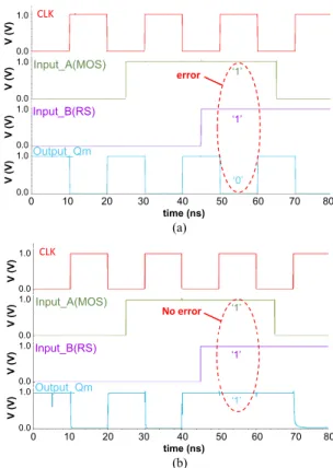
table of the four architectures is always right if resistance comparison between left and right branches is respected (see Tables 2, 3 and 4). Hence, we can simulate the simplified structures (Fig. 4) with STT-MRAM and OxRRAM NVM cells. Figs. 7(a) and 7(b) show the simulation results of Arch.sc with STT-MRAM and OxRRAM elements, respectively.
(a)
(b)
Fig. 7. Transient simulation (Vdd = 1V) for simplified AND logic structure [Arch.sc, Fig. 4(a)] using CMOS 40 nm DK and (a) STT-MRAM compact model, and (b) OxRRAM compact model.
For simulation with STT-MRAM, an error appears when both A and B are in ‘1’ state, which corresponds to the critical
case, where R
ON< RHRS− RLRS must be true. Indeed, as mentioned
in section III, RHRS value of STT-MRAM is inferior to RON,
which imply that the previous condition is not respected. On
the contrary, OxRRAM technology gives higher RHRS (here,
RHRS ≈ 35kΩ) while maintaining relatively low RLRS value
(here, RLRS ≈ 10kΩ) and confirming correct AND operation for
the whole truth table. To solve this issue for STT-MRAM, we show in section III that a second simplified architecture [Arch.s, Fig. 4(b)] can replace Arch. 1 to 4. Transient simulation results of this structure confirm that using
STT-MRAM and more generally any structure where RHRS>RLRS,
always give correct results with Arch.s due to the differential sensing between left and right branches of our structure.
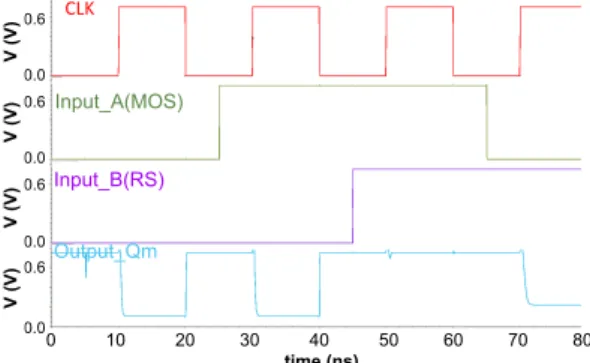
Moreover, as the sensing operation only depend on resistance comparison between left and right branches, it can be interesting to reduce the voltage during operation. Fig. 8 shows the simulation results of Arch.sc with OxRRAM NVM cells for a reading voltage equal to 0.75V instead of 1.0V.
These results prove that our simplified RS-NVLG always works even if lower reading voltage is applied while condition
Metal
IL
active materials: TiOx, Ta2O5, HfO2
Metal TE BE Memory cell CLK$ Input_A(MOS) Input_B(RS) Output_Qm 1.0 0.0 1.0 0.0 1.0 0.0 1.0 0.0 V (V) V (V) V (V) V (V) 0 10 20 30 40 50 60 70 80 time (ns) error$ ‘1’ ‘1’ ‘0’ ‘1’ ‘1’ ‘1’ No#error# CLK$ Input_A(MOS) Input_B(RS) Output_Qm 1.0 0.0 1.0 0.0 1.0 0.0 1.0 0.0 V (V) V (V) V (V) V (V) 0 10 20 30 40 50 60 70 80 time (ns)
R
ON< R
HRS− R
LRS is respected. Other simulations are underinvestigation regarding the resistance ratio versus voltage reading to drawn a generalized conclusion using Arc.sc [Fig. 4(a)] with RS-NVMs.
Fig. 8. Transient simulation for simplified AND logic structure [Arch.sc, Fig. 4(a)] using CMOS 40 nm DK and OxRRAM compact model (Vdd = 0.75V).
B. Architecture validity on read phase
Finally, it is important to note that a precise programming phase is essential to protect the circuit’s functionalities. Indeed, the programming phase, i.e. the current and/or voltage across
NVM cells, will fix the resistance values of RHRS and RLRS.
Hence, the sense amplifier need to be disconnected to the left and right branches of the structure (adding one switch transistor on each branch) when NVM cells are programmed in order to prevent current leakage through outputs. Moreover, as emerging NVM technologies, like STT-MRAM and OxRRAM, suffer from important process variation [8],
variability can be important for RHRS and RLRS values thus write
circuit transistor size and Vdda must be adapted to ensure the largest resistance ratio. We show that we can keep the same
Vdd voltage (1V) using Arch.sc with OxRRAM cells while
over-sizing write transistors.
Due to its non-volatility, standby-power of this synchronous logic gate design can be significantly reduced. It also has advantageous performances in terms of data transfer energy (<fJ/bit) thanks to the shorter distance between memory and computing unit. Although its speed of operation (1 ns) is just comparable to that of conventional CMOS only structure, its density can also be improved by 3D integration of NVM. Furthermore, as the programming frequency of NVM is considerably lower than the computing frequency, the switching power plays an insignificant role in the whole power consumption [25].
VI. CONCLUSION AND PERSPECTIVE
This paper describes an analytical study of synchronous logic gate design based on hybrid architecture with MOS and resistive switching non-volatile memories. From the theory of Boolean equations, we show that two input basic gates (NAND, AND, NOR and OR) can be implemented with very simple structures with a few numbers of MOS transistors and two RS-NVMs. The differential sensing process between the two branches of the structure allows different optimized solutions according to the resistance values of the NVM cells. By using our STT-MRAM and OxRRAM compact models, we successfully simulated AND logic structure as an example to
validate the functionality of RS non-volatile logic gates during both the reading and programming phase. The prototypes are under development in our groups.
ACKNOWLEDGMENT
The authors wish to acknowledge support the French national projects NANOINNOV-SPIN, CNRS-PEPS-NVCPU, ANR-MARS, ANR-DIPMEM.
REFERENCES
[1] International Roadmap for semiconductor (ITRS), 2011 ERD Update. [2] C. Chappert, A. Fert and F. Nguyen Van Dau, “The emergence of spin
electronics in data storage”, Nat. Mater., vol. 6, pp. 813-823, 2007. [3] I.G. Baek et al., “Multi-layer cross-point binary oxide resistive memory
(OxRRAM) for post-NAND storage application”, IEDM Tech. Dig., pp. 750-753, December 2005.
[4] K. Tsuchida et al., “A 64Mb MRAM with clamped-reference and adequate-reference schemes”, Procs. of ISSCC, pp. 258-259, 2010. [5] A. Kawahara et al., “An 8Mb Multi-layered Cross-Point ReRAM Macro
With 443MB/s Write Troughput”, IEEE Journal of Solid-State Circuits, vol. 48, no. 1, pp. 178-185, 2013.
[6] W. Zhao et al., “Synchronous Non-Volatile Logic Gate Design based on Resistive Switching Memories”, Accepted by IEEE Transactions on
Circuits and Systems I, 2013.
[7] S. Matsunaga et al., "Fabrication of a Nonvolatile Full Adder Based on Logic-in-Memory Architecture Using Magnetic Tunnel Junctions",
Appl. Phys. Express, Vol. 1, p. 091301, 2008.
[8] W.S. Zhao et al., “New non-volatile logic based on spin-MTJ”, Physica
Status Solidi-A, vol. 6, pp. 1373-1377, 2008.
[9] S. Onkaraiah et al., “Bipolar ReRAM based non-volatile flip-flops for low-power architectures”, Procs. of NEWCAS, pp. 417-420, 2012. [10] Y. Gang et al., “A High-Reliability, Low-Power Magnetic Full Adder”,
IEEE Transactions on Magnetics., Vol.47, pp.4611-4616, 2011.
[11] H-P Trinh et al., “Magnetic Adder based on racetrack memory”, IEEE
Transactions on Circuits and Systems I, vol.60, pp.1469-1477, 2013.
[12] CMOS40 Design Rule Manual (STMicroelectronics, 2012).
[13] Y. Zhang et al., “Compact modeling of perpendicular-anisotropy CoFeB/MgO magnetic tunnel junctions”, IEEE Trans. Electron
Devices, vol. 59, no. 3, pp. 819-826, 2012.
[14] H. Aziza et al., “Evaluation of OxRAM Cell Variability Impact on Memory Performances through Electrical Simulations”, Non-Volatile
Memory Technology Symposium (NVMTS), January 2011.
[15] W.S. Zhao et al., “High speed, high stability and low power sensing amplifier for MTJ/CMOS hybrid logic circuits”, IEEE Trans. Magn., vol. 45, no. 10, pp. 3784-3787, 2009.
[16] S. Yuasa et al., “Giant room-temperature magnetoresistance in single-crystal Fe/MgO/Fe magnetic tunnel junctions”, Nat. Mater., vol. 3, pp. 868-871, 2004.
[17] S. Ikeda et al., “A perpendicular-anisotropy CoFeB–MgO magnetic tunnel junction”, Nat. Mater., vol. 9, pp. 721-724, 2010.
[18] R. Waser, M. Aono, “Nanoionics-based resistive switching memories”,
Nature Materials, vol.6, pp. 833, 2007.
[19] S. Seo et al., “Reproducible resistance switching in polycrystalline NiO films”, Appl. Phys. Lett., vol. 85, pp. 5655, October 2004.
[20] W. G. Kim et al., “Dependence of the switching characteristics of resistance random access memory on the type of transition metal oxide”,
Procs of ESSDERC, pp. 400-403, November 2010.
[21] Y. Lakys et al., “Self-Enabled “Error-Free” Switching circuit for spin transfer torque MRAM and logic”, IEEE Trans. Magn., vol. 48, pp. 2403-2406, 2012.
[22] H. Y. Lee et al., “Low Power and High Speed Bipolar Switching with A Thin Reactive Ti Buffer Layer in Robust HfO2 Based RRAM”, Procs of
IEDM, pp. 1-4, December 2008.
[23] H. Y. Lee et al., “Low-Power and Nanosecond Switching in Robust Hafnium Oxide Resistive Memory With a Thin Ti Cap,” IEEE Electron
Device Lett., vol. 31, pp. 44–46, January 2010.
[24] C. Cagli et al., “Experimental and Theoretical Study of Electrode Effects in HfO2 based RRAM”, Procs. of IEDM, pp. 28.7.1-28.7.4, 2011. [25] E. Deng et al., “Low Power Magnetic Full-Adder Based on Spin
Transfer Torque MRAM”, Accepted by IEEE Trans. Magn.2013.
CLK$ Input_A(MOS) Input_B(RS) 0.6 0.0 0.6 0.0 0.6 0.0 0.6 0.0 V (V) V (V) V (V) V (V) 0 10 20 30 40 50 60 70 80 time (ns) Output_Qm